US8540888B1 - Methods of patterning layered-material and forming imprinting mold - Google Patents
Methods of patterning layered-material and forming imprinting mold Download PDFInfo
- Publication number
- US8540888B1 US8540888B1 US13/609,854 US201213609854A US8540888B1 US 8540888 B1 US8540888 B1 US 8540888B1 US 201213609854 A US201213609854 A US 201213609854A US 8540888 B1 US8540888 B1 US 8540888B1
- Authority
- US
- United States
- Prior art keywords
- substituted
- group
- independently represents
- atom
- oxygen atom
- Prior art date
- Legal status (The legal status is an assumption and is not a legal conclusion. Google has not performed a legal analysis and makes no representation as to the accuracy of the status listed.)
- Expired - Fee Related
Links
- 0 *.*.*C1=C(C)CCCC1=C.C[1*]C.[2*]C1=C(C)CCCC1=C Chemical compound *.*.*C1=C(C)CCCC1=C.C[1*]C.[2*]C1=C(C)CCCC1=C 0.000 description 35
- XLYJVJLGHZAJAV-JQVHYLCPSA-N CC(C)(C1CCC2(CC1)OC(=O)CC(=O)O2)C1(F)CCC2(CC1)OC(=O)CC(=O)O2.CC(C)(C1CCC2(CC1)OC(=O)CC(=O)O2)C1CCC2(CC1)OC(=O)CC(=O)O2.CCN(CC)C1=CC=C(C=C2C(=O)OC3(CCC(C4CCC5(CC4)OC(=O)C(=CC4=CC=C(N(CC)CC)C=C4)C(=O)O5)CC3)OC2=O)C=C1.O=C1C=C(=O)OC2(CCC(OC3CCC4(CC3)OC(=O)C=C(=O)O4)CC2)O1.O=C1CC(=O)OC2(CCC(C3CCC4(CC3)OC(=O)CC(=O)O4)CC2)O1.O=C1CC(=O)OC2(CCC(S(=O)(=O)C3CCC4(CC3)OC(=O)CC(=O)O4)CC2)O1.[C-]#[N+]/C(C#N)=C1/C/C(=C(\C#N)[N+]#[C-])OC2(CCC(C(C)(C)C3CCC4(CC3)O/C(=C(\C#N)[N+]#[C-])C/C(=C(/C#N)[N+]#[C-])O4)CC2)O1.[C-]#[N+]/C(C#N)=C1/CC(=O)OC2(CCC(C(C)(C)C3CCC4(CC3)OC(=O)C/C(=C(/C#N)[N+]#[C-])O4)CC2)O1 Chemical compound CC(C)(C1CCC2(CC1)OC(=O)CC(=O)O2)C1(F)CCC2(CC1)OC(=O)CC(=O)O2.CC(C)(C1CCC2(CC1)OC(=O)CC(=O)O2)C1CCC2(CC1)OC(=O)CC(=O)O2.CCN(CC)C1=CC=C(C=C2C(=O)OC3(CCC(C4CCC5(CC4)OC(=O)C(=CC4=CC=C(N(CC)CC)C=C4)C(=O)O5)CC3)OC2=O)C=C1.O=C1C=C(=O)OC2(CCC(OC3CCC4(CC3)OC(=O)C=C(=O)O4)CC2)O1.O=C1CC(=O)OC2(CCC(C3CCC4(CC3)OC(=O)CC(=O)O4)CC2)O1.O=C1CC(=O)OC2(CCC(S(=O)(=O)C3CCC4(CC3)OC(=O)CC(=O)O4)CC2)O1.[C-]#[N+]/C(C#N)=C1/C/C(=C(\C#N)[N+]#[C-])OC2(CCC(C(C)(C)C3CCC4(CC3)O/C(=C(\C#N)[N+]#[C-])C/C(=C(/C#N)[N+]#[C-])O4)CC2)O1.[C-]#[N+]/C(C#N)=C1/CC(=O)OC2(CCC(C(C)(C)C3CCC4(CC3)OC(=O)C/C(=C(/C#N)[N+]#[C-])O4)CC2)O1 XLYJVJLGHZAJAV-JQVHYLCPSA-N 0.000 description 1
- HLZOOBSHUFVABM-WVXPDVSNSA-N CC(C)OC(=O)C1=CC=C(CN2C3=C(C=CC=C3)C(C)(C)/C2=C\C=C2C(=O)OC3(OC2=O)C2CC4CC(C2)CC3C4)C=C1.CCCCN1C2=C(C=CC=C2)C(C)(C)/C1=C\C=C1C(=O)OC2(CCCC2)OC1=O.CCCCN1C2=C(C=CC=C2)C(C)(C)/C1=C\C=C1C(=O)OC2(OC1=O)C1CC3CC(C1)CC2C3.[C-]#[N+]/C(C#N)=C1/OC(C)(C)O/C(=C(\C#N)[N+]#[C-])C1=C/C=C1/N(CCCC)C2=C(C=CC=C2)C1(C)C Chemical compound CC(C)OC(=O)C1=CC=C(CN2C3=C(C=CC=C3)C(C)(C)/C2=C\C=C2C(=O)OC3(OC2=O)C2CC4CC(C2)CC3C4)C=C1.CCCCN1C2=C(C=CC=C2)C(C)(C)/C1=C\C=C1C(=O)OC2(CCCC2)OC1=O.CCCCN1C2=C(C=CC=C2)C(C)(C)/C1=C\C=C1C(=O)OC2(OC1=O)C1CC3CC(C1)CC2C3.[C-]#[N+]/C(C#N)=C1/OC(C)(C)O/C(=C(\C#N)[N+]#[C-])C1=C/C=C1/N(CCCC)C2=C(C=CC=C2)C1(C)C HLZOOBSHUFVABM-WVXPDVSNSA-N 0.000 description 1
- LWLHHEHXVANRQY-HBJVCFLDSA-N CC1(C)C2=C(C=CC=C2)N(CC2=C(F)C(F)=C(F)C(F)=C2F)/C1=C/C=C1C(=O)OC2(OC1=O)C1CC3CC(C1)CC2C3.CCCCCCCCN1C2=C(C=CC(F)=C2)C(C)(C)/C1=C\C=C1C(=O)OC2(CCCCC2)OC1=O.CCCN1C2=C(C=C(Cl)C=C2)C(C)(C)/C1=C\C=C1C(=O)CCCC1=O.CCCN1C2=C(C=CC([N+](=O)[O-])=C2)C(C)(C)/C1=C\C=C1C(=O)CCCC1=O Chemical compound CC1(C)C2=C(C=CC=C2)N(CC2=C(F)C(F)=C(F)C(F)=C2F)/C1=C/C=C1C(=O)OC2(OC1=O)C1CC3CC(C1)CC2C3.CCCCCCCCN1C2=C(C=CC(F)=C2)C(C)(C)/C1=C\C=C1C(=O)OC2(CCCCC2)OC1=O.CCCN1C2=C(C=C(Cl)C=C2)C(C)(C)/C1=C\C=C1C(=O)CCCC1=O.CCCN1C2=C(C=CC([N+](=O)[O-])=C2)C(C)(C)/C1=C\C=C1C(=O)CCCC1=O LWLHHEHXVANRQY-HBJVCFLDSA-N 0.000 description 1
- UIEQEJJRZXDXTJ-PUWDXADISA-N CC1(C)C2=C(C=CC=C2)N(CCCCN2C3=C(C=CC=C3)C(C)(C)/C2=C\C=C2C(=O)OC3(OC2=O)C2CC4CC(C2)CC3C4)/C1=C\C=C1C(=O)OC2(OC1=O)C1CC3CC(C1)CC2C3 Chemical compound CC1(C)C2=C(C=CC=C2)N(CCCCN2C3=C(C=CC=C3)C(C)(C)/C2=C\C=C2C(=O)OC3(OC2=O)C2CC4CC(C2)CC3C4)/C1=C\C=C1C(=O)OC2(OC1=O)C1CC3CC(C1)CC2C3 UIEQEJJRZXDXTJ-PUWDXADISA-N 0.000 description 1
- RKEPDGWXNRCCQI-LIXXLMIQSA-N CC1(C)C2=C(C=CC=C2)N(CCCCS(=O)(=O)O)/C1=C/CC1SC(=S)N(CCC(=O)O)C1=O.COC(=O)C1=CC=C(CN2C3=C(C=CC=C3)C(C)(C)/C2=C\C=C2/NC(=S)NC2=O)C=C1.COC(=O)C1=CC=C(CN2C3=C(C=CC=C3)C(C)(C)/C2=C\CC2SC(=S)N(CC(=O)O)C2=O)C=C1 Chemical compound CC1(C)C2=C(C=CC=C2)N(CCCCS(=O)(=O)O)/C1=C/CC1SC(=S)N(CCC(=O)O)C1=O.COC(=O)C1=CC=C(CN2C3=C(C=CC=C3)C(C)(C)/C2=C\C=C2/NC(=S)NC2=O)C=C1.COC(=O)C1=CC=C(CN2C3=C(C=CC=C3)C(C)(C)/C2=C\CC2SC(=S)N(CC(=O)O)C2=O)C=C1 RKEPDGWXNRCCQI-LIXXLMIQSA-N 0.000 description 1
- DXOABCKLSFUBPS-ITDMVWFMSA-N CC1(C)C2=C(C=CC=C2)[N+]2=C1/C=C/C1=C([O-])OC3(CCC(CC3)C3CCC4(CC3)OC(=O)C(=C(/[O-])O4)/C=C/C3=[N+](CCCCCCCC[N+]4=C(/C=C/C5=C(=[O-])OC6(CCC(CC6)C6CCC7(CC6)OC(=O)C(=C(=[O-])O7)/C=C/C6=[N+](CCCCCCCC2)C2=C(C=CC=C2)C6(C)C)OC5=O)C(C)(C)C2=C4C=CC=C2)C2=C(C=CC=C2)C3(C)C)OC1=O.CC1(C)CO/C(=C/C=C2C(=O)OC3(CCC(CC4CCC5(CC4)OC(=O)C(=C/C=C4/OCC(C)(C)N4CC4=C(F)C(F)=C(F)C(F)=C4F)C(=O)O5)CC3)OC2=O)N1CC1=C(F)C(F)=C(F)C(F)=C1F.[C-]#[N+]/C(C#N)=C1\OC2(CCC(C3CCC4(CC3)OC([O-])=C(/C=C/C3=[N+](\CC5=CC=C(C(=O)OC)C=C5)C5=C(C=CC=C5)C3(C)C)/C(=C(/C#N)[N+]#[C-])O4)CC2)OC([O-])=C1/C=C/C1=[N+](\CC2=CC=C(C(=O)CO)C=C2)C2=C(C=CC=C2)C1(C)C.[H]N1C(=O)C(=C/C=C2/SC3=C(C=CC=C3)N2CCCC)C(=O)N([H])C12CCC(CC1CCC3(CC1)N([H])C(=O)C(=C/C=C1/SC4=C(C=CC=C4)N1CCCC)C(=O)N3[H])CC2 Chemical compound CC1(C)C2=C(C=CC=C2)[N+]2=C1/C=C/C1=C([O-])OC3(CCC(CC3)C3CCC4(CC3)OC(=O)C(=C(/[O-])O4)/C=C/C3=[N+](CCCCCCCC[N+]4=C(/C=C/C5=C(=[O-])OC6(CCC(CC6)C6CCC7(CC6)OC(=O)C(=C(=[O-])O7)/C=C/C6=[N+](CCCCCCCC2)C2=C(C=CC=C2)C6(C)C)OC5=O)C(C)(C)C2=C4C=CC=C2)C2=C(C=CC=C2)C3(C)C)OC1=O.CC1(C)CO/C(=C/C=C2C(=O)OC3(CCC(CC4CCC5(CC4)OC(=O)C(=C/C=C4/OCC(C)(C)N4CC4=C(F)C(F)=C(F)C(F)=C4F)C(=O)O5)CC3)OC2=O)N1CC1=C(F)C(F)=C(F)C(F)=C1F.[C-]#[N+]/C(C#N)=C1\OC2(CCC(C3CCC4(CC3)OC([O-])=C(/C=C/C3=[N+](\CC5=CC=C(C(=O)OC)C=C5)C5=C(C=CC=C5)C3(C)C)/C(=C(/C#N)[N+]#[C-])O4)CC2)OC([O-])=C1/C=C/C1=[N+](\CC2=CC=C(C(=O)CO)C=C2)C2=C(C=CC=C2)C1(C)C.[H]N1C(=O)C(=C/C=C2/SC3=C(C=CC=C3)N2CCCC)C(=O)N([H])C12CCC(CC1CCC3(CC1)N([H])C(=O)C(=C/C=C1/SC4=C(C=CC=C4)N1CCCC)C(=O)N3[H])CC2 DXOABCKLSFUBPS-ITDMVWFMSA-N 0.000 description 1
- CXHVZSDHKNVNHG-LIRVSWQRSA-N CC1=C(/N=N/C2=C(O)NC3(NC2=O)C2CC4CC(C2)CC3C4)C(=O)N(C2=CC=CC=C2)N1C.CC1=C(/N=N/C2=C(O)OC(C)(C)NC2=O)C(=O)N(C2=CC=CC=C2)N1C.CC1=C(/N=N/C2=C(O)OC(C)(C)OC2C)C(=O)N(C2=CC=CC=C2)N1C.CC1=C(/N=N/C2=C(O)OC(C)(C3=CC=CC=C3)OC2C)C(=O)N(C2=CC=CC=C2)N1C.CC1=C(/N=N/C2=C(O)OC3(OC2=O)C2CC4CC(C2)CC3C4)C(=O)N(C2=CC=CC=C2)N1C.CCC1(C)OC(=O)C(/N=N/C2=C(C)N(C)N(C3=CC=CC=C3)C2=O)=C(O)O1 Chemical compound CC1=C(/N=N/C2=C(O)NC3(NC2=O)C2CC4CC(C2)CC3C4)C(=O)N(C2=CC=CC=C2)N1C.CC1=C(/N=N/C2=C(O)OC(C)(C)NC2=O)C(=O)N(C2=CC=CC=C2)N1C.CC1=C(/N=N/C2=C(O)OC(C)(C)OC2C)C(=O)N(C2=CC=CC=C2)N1C.CC1=C(/N=N/C2=C(O)OC(C)(C3=CC=CC=C3)OC2C)C(=O)N(C2=CC=CC=C2)N1C.CC1=C(/N=N/C2=C(O)OC3(OC2=O)C2CC4CC(C2)CC3C4)C(=O)N(C2=CC=CC=C2)N1C.CCC1(C)OC(=O)C(/N=N/C2=C(C)N(C)N(C3=CC=CC=C3)C2=O)=C(O)O1 CXHVZSDHKNVNHG-LIRVSWQRSA-N 0.000 description 1
- UORBFOUWHUMKQK-QYGBBDPSSA-N CC1=C(/N=N/C2=C(O)OC(C)(C)CC2=O)C(=O)N(C2=CC=CC=C2)N1C.CC1=C(/N=N/C2=C(O)OC3(CCCCC3)OC2=O)C(=O)N(C2=CC=CC=C2)N1C.CCN1C(=O)C(/N=N/C2=C(C)N(C)N(C3=CC=CC=C3)C2=O)=C(O)N(CC)C1=S.[C-]#[N+]/C(C#N)=C1/OC2(OC(O)=C1/N=N/C1=C(C)N(C)N(C3=CC=CC=C3)C1=O)C1CC3CC(C1)CC2C3 Chemical compound CC1=C(/N=N/C2=C(O)OC(C)(C)CC2=O)C(=O)N(C2=CC=CC=C2)N1C.CC1=C(/N=N/C2=C(O)OC3(CCCCC3)OC2=O)C(=O)N(C2=CC=CC=C2)N1C.CCN1C(=O)C(/N=N/C2=C(C)N(C)N(C3=CC=CC=C3)C2=O)=C(O)N(CC)C1=S.[C-]#[N+]/C(C#N)=C1/OC2(OC(O)=C1/N=N/C1=C(C)N(C)N(C3=CC=CC=C3)C1=O)C1CC3CC(C1)CC2C3 UORBFOUWHUMKQK-QYGBBDPSSA-N 0.000 description 1
- PHILPPYNEVPFBK-GGYWYYNMSA-K CC1=C(/N=N/C2=C(O)OC3(CCC(C(C)(C)C4CCC5(CC4)OC(=O)C(/N=N/C4=C(C)N(C)N(C6=CC=CC=C6)C4=O)=C(O)O5)CC3)OC2=O)C(=O)N(C2=CC=CC=C2)N1C.CC1=C2/N=N/C3=C4/OC5(CCC(CC5)C(C)(C)C5CCC6(CC5)OC(=O)C5=C(\O6)O[Ni@@]6(OC7=C(/N=N/C8=C(C)N(C)N(C9=CC=CC=C9)/C8=O/6)C(=O)OC6(CCC(CC6)C(C)(C)C6CCC8(CC6)OC(=O)C6/N=N/C9=C(C)N(C)N(C%10=CC=CC=C%10)/C9=O/[Ni@@](O4)(OC6O8)/O=C\2N(C2=CC=CC=C2)N1C)O7)/O=C1\C(=C(C)N(C)N1C1=CC=CC=C1)\N=N\5)OC3=O.CC1=CC(/N=N/C2=C(O)OC3(CCC(C(C)(C)C4CCC5(CC4)OC(=O)C(/N=N/C4=NOC(C)=C4)=C(O)O5)CC3)OC2=O)=NO1.COC1=CC2=C(C=C1)N=C(/N=N/C1=C(O)OC3(CCC(C4CCC5(CC4)OC(=O)C(/N=N/C4=NC6=C(C=C(OC)C=C6)S4)=C(O)O5)CC3)OC1=O)S2.COC1=CC=C(NC2=CC=C(/N=N/C3=C(O)OC4(CCC(C5CCC6(CC5)OC(=O)C(/N=N/C5=CC=C(NC7=CC=C(CO)C=C7)C=C5)=C(O)O6)CC4)OC3=O)C=C2)C=C1 Chemical compound CC1=C(/N=N/C2=C(O)OC3(CCC(C(C)(C)C4CCC5(CC4)OC(=O)C(/N=N/C4=C(C)N(C)N(C6=CC=CC=C6)C4=O)=C(O)O5)CC3)OC2=O)C(=O)N(C2=CC=CC=C2)N1C.CC1=C2/N=N/C3=C4/OC5(CCC(CC5)C(C)(C)C5CCC6(CC5)OC(=O)C5=C(\O6)O[Ni@@]6(OC7=C(/N=N/C8=C(C)N(C)N(C9=CC=CC=C9)/C8=O/6)C(=O)OC6(CCC(CC6)C(C)(C)C6CCC8(CC6)OC(=O)C6/N=N/C9=C(C)N(C)N(C%10=CC=CC=C%10)/C9=O/[Ni@@](O4)(OC6O8)/O=C\2N(C2=CC=CC=C2)N1C)O7)/O=C1\C(=C(C)N(C)N1C1=CC=CC=C1)\N=N\5)OC3=O.CC1=CC(/N=N/C2=C(O)OC3(CCC(C(C)(C)C4CCC5(CC4)OC(=O)C(/N=N/C4=NOC(C)=C4)=C(O)O5)CC3)OC2=O)=NO1.COC1=CC2=C(C=C1)N=C(/N=N/C1=C(O)OC3(CCC(C4CCC5(CC4)OC(=O)C(/N=N/C4=NC6=C(C=C(OC)C=C6)S4)=C(O)O5)CC3)OC1=O)S2.COC1=CC=C(NC2=CC=C(/N=N/C3=C(O)OC4(CCC(C5CCC6(CC5)OC(=O)C(/N=N/C5=CC=C(NC7=CC=C(CO)C=C7)C=C5)=C(O)O6)CC4)OC3=O)C=C2)C=C1 PHILPPYNEVPFBK-GGYWYYNMSA-K 0.000 description 1
- YIPPDUZUIGRHLK-XTRFFESWSA-J CC1=C2/N=N/C3=C(NC4(NC3=O)C3CC5CC(C3)CC4C5)O[Cu]3(OC4=C(/N=N/C5=C(C)N(C)N(C6=CC=CC=C6)/C5=O/3)C(=O)NC3(N4)C4CC5CC(C4)CC3C5)/O=C\2N(C2=CC=CC=C2)N1C.CC1=C2/N=N/C3=C(NC4(NC3=O)C3CC5CC(C3)CC4C5)O[Zn]3(OC4=C(/N=N/C5=C(C)N(C)N(C6=CC=CC=C6)/C5=O/3)C(=O)NC3(N4)C4CC5CC(C4)CC3C5)/O=C\2N(C2=CC=CC=C2)N1C Chemical compound CC1=C2/N=N/C3=C(NC4(NC3=O)C3CC5CC(C3)CC4C5)O[Cu]3(OC4=C(/N=N/C5=C(C)N(C)N(C6=CC=CC=C6)/C5=O/3)C(=O)NC3(N4)C4CC5CC(C4)CC3C5)/O=C\2N(C2=CC=CC=C2)N1C.CC1=C2/N=N/C3=C(NC4(NC3=O)C3CC5CC(C3)CC4C5)O[Zn]3(OC4=C(/N=N/C5=C(C)N(C)N(C6=CC=CC=C6)/C5=O/3)C(=O)NC3(N4)C4CC5CC(C4)CC3C5)/O=C\2N(C2=CC=CC=C2)N1C YIPPDUZUIGRHLK-XTRFFESWSA-J 0.000 description 1
- IUHLDIYCWICMMD-IOHQKBGHSA-H CC1=C2/N=N/C3=C(NC4(NC3=O)C3CC5CC(C3)CC4C5)O[Fe]3(OC4=C(/N=N/C5=C(C)N(C)N(C6=CC=CC=C6)/C5=O/3)C(=O)NC3(N4)C4CC5CC(C4)CC3C5)/O=C\2N(C2=CC=CC=C2)N1C.CC1=C2/N=N/C3=C(OC4(OC3=O)C3CC5CC(C3)CC4C5)O[Co]3(OC4=C(/N=N/C5=C(C)N(C)N(C6=CC=CC=C6)/C5=O/3)C(=O)OC3(O4)C4CC5CC(C4)CC3C5)/O=C\2N(C2=CC=CC=C2)N1C.CC1=C2/N=N/C3=C(OC4(OC3=O)C3CC5CC(C3)CC4C5)O[Ni]3(OC4=C(/N=N/C5=C(C)N(C)N(C6=CC=CC=C6)/C5=O/3)C(=O)OC3(O4)C4CC5CC(C4)CC3C5)/O=C\2N(C2=CC=CC=C2)N1C Chemical compound CC1=C2/N=N/C3=C(NC4(NC3=O)C3CC5CC(C3)CC4C5)O[Fe]3(OC4=C(/N=N/C5=C(C)N(C)N(C6=CC=CC=C6)/C5=O/3)C(=O)NC3(N4)C4CC5CC(C4)CC3C5)/O=C\2N(C2=CC=CC=C2)N1C.CC1=C2/N=N/C3=C(OC4(OC3=O)C3CC5CC(C3)CC4C5)O[Co]3(OC4=C(/N=N/C5=C(C)N(C)N(C6=CC=CC=C6)/C5=O/3)C(=O)OC3(O4)C4CC5CC(C4)CC3C5)/O=C\2N(C2=CC=CC=C2)N1C.CC1=C2/N=N/C3=C(OC4(OC3=O)C3CC5CC(C3)CC4C5)O[Ni]3(OC4=C(/N=N/C5=C(C)N(C)N(C6=CC=CC=C6)/C5=O/3)C(=O)OC3(O4)C4CC5CC(C4)CC3C5)/O=C\2N(C2=CC=CC=C2)N1C IUHLDIYCWICMMD-IOHQKBGHSA-H 0.000 description 1
- GBTCFTCZZNIVLQ-POEIKCKHSA-N CC1CC2(CCC1C(C)(C)C1CCC3(CC1C)OC(=O)CC(=O)O3)OC(=O)CC(=O)O2.CCCC/[N+]1=C(\C=C\C2=C([O-])OC3(CCC(C(C)(C)C4CCC5(CC4)OC(=O)C(/C=C/C4=[N+](\CCCC)C6=C(C=CC=C6)C4(C)C)=C([O-])O5)CC3)OC2=O)C(C)(C)C2=C1C=CC=C2.CCN(CC)C1=CC=C(C=C2C(=O)OC3(CCC(C(C)(C)C4CCC5(CC4)OC(=O)C(=CC4=CC=C(N(CC)CC)C=C4)C(=O)O5)CC3)OC2=O)C=C1.COC(=O)C1=CC=C(C/[N+]2=C(\C=C\C3=C([O-])OC4(CCC(C5CCC6(CC5)OC(=O)C(/C=C/C5=[N+](\CC7=CC=C(C(=O)CO)C=C7)C7=C(C=CC=C7)C5(C)C)=C([O-])O6)CC4)OC3=O)C(C)(C)C3=C2C=CC=C3)C=C1.O=C1C=C(=O)OC2(CCC(C3CCC4(CC3)NC(=O)C=C(=O)O4)CC2)N1 Chemical compound CC1CC2(CCC1C(C)(C)C1CCC3(CC1C)OC(=O)CC(=O)O3)OC(=O)CC(=O)O2.CCCC/[N+]1=C(\C=C\C2=C([O-])OC3(CCC(C(C)(C)C4CCC5(CC4)OC(=O)C(/C=C/C4=[N+](\CCCC)C6=C(C=CC=C6)C4(C)C)=C([O-])O5)CC3)OC2=O)C(C)(C)C2=C1C=CC=C2.CCN(CC)C1=CC=C(C=C2C(=O)OC3(CCC(C(C)(C)C4CCC5(CC4)OC(=O)C(=CC4=CC=C(N(CC)CC)C=C4)C(=O)O5)CC3)OC2=O)C=C1.COC(=O)C1=CC=C(C/[N+]2=C(\C=C\C3=C([O-])OC4(CCC(C5CCC6(CC5)OC(=O)C(/C=C/C5=[N+](\CC7=CC=C(C(=O)CO)C=C7)C7=C(C=CC=C7)C5(C)C)=C([O-])O6)CC4)OC3=O)C(C)(C)C3=C2C=CC=C3)C=C1.O=C1C=C(=O)OC2(CCC(C3CCC4(CC3)NC(=O)C=C(=O)O4)CC2)N1 GBTCFTCZZNIVLQ-POEIKCKHSA-N 0.000 description 1
- AGGLSMQPFICFGR-SKNGEXPGSA-N CCCCN1/C(=C/C=C2C(=O)OC(C)(C)OC2=O)OCC1(C)C.CCCCN1C2=C(C3=C(C=CC=C3)C=C2)C(C)(C)/C1=C\C=C1C(=O)OC2(OC1=O)C1CC3CC(C1)CC2C3.CCCCN1C2=C(C=CC=C2)C(C)(C)/C1=C\C=C1C(=O)OC(C)(C2=CC=CC=C2)OC1=O.COC(=O)C1=CC=C(CN2C3=C(C=CC=C3)C(C)(C)/C2=C\C=C2C(=O)OC3(OC2=O)C2CC4CC(C2)CC3C4)C=C1 Chemical compound CCCCN1/C(=C/C=C2C(=O)OC(C)(C)OC2=O)OCC1(C)C.CCCCN1C2=C(C3=C(C=CC=C3)C=C2)C(C)(C)/C1=C\C=C1C(=O)OC2(OC1=O)C1CC3CC(C1)CC2C3.CCCCN1C2=C(C=CC=C2)C(C)(C)/C1=C\C=C1C(=O)OC(C)(C2=CC=CC=C2)OC1=O.COC(=O)C1=CC=C(CN2C3=C(C=CC=C3)C(C)(C)/C2=C\C=C2C(=O)OC3(OC2=O)C2CC4CC(C2)CC3C4)C=C1 AGGLSMQPFICFGR-SKNGEXPGSA-N 0.000 description 1
- YAAVSGUHTGASJL-HQEPYBGCSA-N CCCCN1C2=C(C3=C(C=CC=C3)C=C2)C(C)(C)/C1=C\C=C1C(=O)OC2(CCC3(CC2)OC(=O)C(=C/C=C2/N(CCCC)C4=C(C5=C(C=CC=C5)C=C4)C2(C)C)C(=O)O3)OC1=O.CCCCN1C2=C(C=CC(OC)=C2)[Se]/C1=C\C=C1C(=O)OC2(CCC3(CC2)OC(=O)C(=C/C=C2\[Se]C4=C(C=C(OC)C=C4)N2CCCC)C(=O)O3)OC1=O.COC(=O)C1=CC=C(CN2C3=C(C=CC=C3)C(C)(C)/C2=C\C=C2C(=O)OC3(CCC4(CC3)OC(=O)C(=C/C=C3/N(CC5=CC=C(C(=O)CO)C=C5)C5=C(C=CC=C5)C3(C)C)C(=O)O4)OC2=O)C=C1 Chemical compound CCCCN1C2=C(C3=C(C=CC=C3)C=C2)C(C)(C)/C1=C\C=C1C(=O)OC2(CCC3(CC2)OC(=O)C(=C/C=C2/N(CCCC)C4=C(C5=C(C=CC=C5)C=C4)C2(C)C)C(=O)O3)OC1=O.CCCCN1C2=C(C=CC(OC)=C2)[Se]/C1=C\C=C1C(=O)OC2(CCC3(CC2)OC(=O)C(=C/C=C2\[Se]C4=C(C=C(OC)C=C4)N2CCCC)C(=O)O3)OC1=O.COC(=O)C1=CC=C(CN2C3=C(C=CC=C3)C(C)(C)/C2=C\C=C2C(=O)OC3(CCC4(CC3)OC(=O)C(=C/C=C3/N(CC5=CC=C(C(=O)CO)C=C5)C5=C(C=CC=C5)C3(C)C)C(=O)O4)OC2=O)C=C1 YAAVSGUHTGASJL-HQEPYBGCSA-N 0.000 description 1
- OXSVMUMKFPHNKI-LGLXDMIVSA-N CCCCN1C2=C(C=CC=C2)C(C)(C)/C1=C\C=C1C(=O)N(C)C(=O)N(C)C1=O.CCCCN1C2=C(C=CC=C2)C(C)(C)/C1=C\C=C1C(=O)N(CC)C(=S)N(CC)C1=O.CCCCN1C2=C(C=CC=C2)C(C)(C)/C1=C\C=C1C(=O)NC2(NC1=O)C1CC3CC(C1)CC2C3.COC(=O)C1=CC=C(CN2C3=C(C=CC=C3)S/C2=C\C=C2C(=O)OC3(OC2=O)C2CC4CC(C2)CC3C4)C=C1 Chemical compound CCCCN1C2=C(C=CC=C2)C(C)(C)/C1=C\C=C1C(=O)N(C)C(=O)N(C)C1=O.CCCCN1C2=C(C=CC=C2)C(C)(C)/C1=C\C=C1C(=O)N(CC)C(=S)N(CC)C1=O.CCCCN1C2=C(C=CC=C2)C(C)(C)/C1=C\C=C1C(=O)NC2(NC1=O)C1CC3CC(C1)CC2C3.COC(=O)C1=CC=C(CN2C3=C(C=CC=C3)S/C2=C\C=C2C(=O)OC3(OC2=O)C2CC4CC(C2)CC3C4)C=C1 OXSVMUMKFPHNKI-LGLXDMIVSA-N 0.000 description 1
- MAWSSOPUURYSIK-UHFFFAOYSA-N CCCC[N+]1=C(/C=C/C2=C([O-])OC3(OC2=O)C2CC4CC(C2)CC3C4)C(C)(C)C2=C1C=CC1=C2C=CC=C1 Chemical compound CCCC[N+]1=C(/C=C/C2=C([O-])OC3(OC2=O)C2CC4CC(C2)CC3C4)C(C)(C)C2=C1C=CC1=C2C=CC=C1 MAWSSOPUURYSIK-UHFFFAOYSA-N 0.000 description 1
- PJPSTITVOIDNTP-ODURILKVSA-J CCN1C(=O)C2=C(O[Cu]3(OC4=C(/N=N/C5=C(C)N(C)N(C6=CC=CC=C6)/C5=O/3)C(=O)N(CC)C(=S)N4CC)/O=C3\C(=C(C)N(C)N3C3=CC=CC=C3)/N=N/2)N(CC)C1=S.CCN1C(=O)C2=C(O[Ni]3(OC4=C(/N=N/C5=C(C)N(C)N(C6=CC=CC=C6)/C5=O/3)C(=O)N(CC)C(=S)N4CC)/O=C3\C(=C(C)N(C)N3C3=CC=CC=C3)/N=N/2)N(CC)C1=S Chemical compound CCN1C(=O)C2=C(O[Cu]3(OC4=C(/N=N/C5=C(C)N(C)N(C6=CC=CC=C6)/C5=O/3)C(=O)N(CC)C(=S)N4CC)/O=C3\C(=C(C)N(C)N3C3=CC=CC=C3)/N=N/2)N(CC)C1=S.CCN1C(=O)C2=C(O[Ni]3(OC4=C(/N=N/C5=C(C)N(C)N(C6=CC=CC=C6)/C5=O/3)C(=O)N(CC)C(=S)N4CC)/O=C3\C(=C(C)N(C)N3C3=CC=CC=C3)/N=N/2)N(CC)C1=S PJPSTITVOIDNTP-ODURILKVSA-J 0.000 description 1
- APHDAXQBHYEWJT-IUEPLBAQSA-K CCOC(=O)CC[N+]1=C(/C=C/C2=C([O-])OC3(CCC(C(C)(C)C4CCC5(CC4)OC(=O)C(=CC4=CC=C(N(CC)CC)C=C4)C(=O)O5)CC3)OC2=O)C(C)(C)C2=C1C=CC=C2.CN/C(C)=C1/N=N/C2=C3/OC4(CCC(CC4)C(C)(C)C4CCC5(CC4)OC(=O)C4=C(\O5)O[Co@@]5(OC6=C(/N=N/C(=C(\C)NC)/C(NC7=CC=CC=C7)=O\5)C(=O)OC5(CCC(CC5)C(C)(C)C5CCC7(CC5)OC(=O)C5/N=N/C(=C(\C)NC)/C(NC8=CC=CC=C8)=O\[Co@@](O3)(OC5O7)\O=C/1NC1=CC=CC=C1)O6)/O=C(NC1=CC=CC=C1)\C(=C(\C)N)\N=N\4)OC2=O.C[N+]1=C(/N=N/C2=C([O-])OC3(CCC(C(C)(C)C4CCC5(CC4)OC(=O)C(/N=N/C4=[N+](C)C6=C(=C4(C)C)C=CC=C6)=C([O-])O5)CC3)OC2=O)C(C)(C)=C2=C1C=CC=C2 Chemical compound CCOC(=O)CC[N+]1=C(/C=C/C2=C([O-])OC3(CCC(C(C)(C)C4CCC5(CC4)OC(=O)C(=CC4=CC=C(N(CC)CC)C=C4)C(=O)O5)CC3)OC2=O)C(C)(C)C2=C1C=CC=C2.CN/C(C)=C1/N=N/C2=C3/OC4(CCC(CC4)C(C)(C)C4CCC5(CC4)OC(=O)C4=C(\O5)O[Co@@]5(OC6=C(/N=N/C(=C(\C)NC)/C(NC7=CC=CC=C7)=O\5)C(=O)OC5(CCC(CC5)C(C)(C)C5CCC7(CC5)OC(=O)C5/N=N/C(=C(\C)NC)/C(NC8=CC=CC=C8)=O\[Co@@](O3)(OC5O7)\O=C/1NC1=CC=CC=C1)O6)/O=C(NC1=CC=CC=C1)\C(=C(\C)N)\N=N\4)OC2=O.C[N+]1=C(/N=N/C2=C([O-])OC3(CCC(C(C)(C)C4CCC5(CC4)OC(=O)C(/N=N/C4=[N+](C)C6=C(=C4(C)C)C=CC=C6)=C([O-])O5)CC3)OC2=O)C(C)(C)=C2=C1C=CC=C2 APHDAXQBHYEWJT-IUEPLBAQSA-K 0.000 description 1
Images


Classifications
-
- G—PHYSICS
- G03—PHOTOGRAPHY; CINEMATOGRAPHY; ANALOGOUS TECHNIQUES USING WAVES OTHER THAN OPTICAL WAVES; ELECTROGRAPHY; HOLOGRAPHY
- G03F—PHOTOMECHANICAL PRODUCTION OF TEXTURED OR PATTERNED SURFACES, e.g. FOR PRINTING, FOR PROCESSING OF SEMICONDUCTOR DEVICES; MATERIALS THEREFOR; ORIGINALS THEREFOR; APPARATUS SPECIALLY ADAPTED THEREFOR
- G03F7/00—Photomechanical, e.g. photolithographic, production of textured or patterned surfaces, e.g. printing surfaces; Materials therefor, e.g. comprising photoresists; Apparatus specially adapted therefor
- G03F7/004—Photosensitive materials
- G03F7/027—Non-macromolecular photopolymerisable compounds having carbon-to-carbon double bonds, e.g. ethylenic compounds
-
- B—PERFORMING OPERATIONS; TRANSPORTING
- B82—NANOTECHNOLOGY
- B82Y—SPECIFIC USES OR APPLICATIONS OF NANOSTRUCTURES; MEASUREMENT OR ANALYSIS OF NANOSTRUCTURES; MANUFACTURE OR TREATMENT OF NANOSTRUCTURES
- B82Y10/00—Nanotechnology for information processing, storage or transmission, e.g. quantum computing or single electron logic
-
- B—PERFORMING OPERATIONS; TRANSPORTING
- B82—NANOTECHNOLOGY
- B82Y—SPECIFIC USES OR APPLICATIONS OF NANOSTRUCTURES; MEASUREMENT OR ANALYSIS OF NANOSTRUCTURES; MANUFACTURE OR TREATMENT OF NANOSTRUCTURES
- B82Y40/00—Manufacture or treatment of nanostructures
-
- G—PHYSICS
- G03—PHOTOGRAPHY; CINEMATOGRAPHY; ANALOGOUS TECHNIQUES USING WAVES OTHER THAN OPTICAL WAVES; ELECTROGRAPHY; HOLOGRAPHY
- G03F—PHOTOMECHANICAL PRODUCTION OF TEXTURED OR PATTERNED SURFACES, e.g. FOR PRINTING, FOR PROCESSING OF SEMICONDUCTOR DEVICES; MATERIALS THEREFOR; ORIGINALS THEREFOR; APPARATUS SPECIALLY ADAPTED THEREFOR
- G03F7/00—Photomechanical, e.g. photolithographic, production of textured or patterned surfaces, e.g. printing surfaces; Materials therefor, e.g. comprising photoresists; Apparatus specially adapted therefor
- G03F7/0002—Lithographic processes using patterning methods other than those involving the exposure to radiation, e.g. by stamping
-
- G—PHYSICS
- G03—PHOTOGRAPHY; CINEMATOGRAPHY; ANALOGOUS TECHNIQUES USING WAVES OTHER THAN OPTICAL WAVES; ELECTROGRAPHY; HOLOGRAPHY
- G03F—PHOTOMECHANICAL PRODUCTION OF TEXTURED OR PATTERNED SURFACES, e.g. FOR PRINTING, FOR PROCESSING OF SEMICONDUCTOR DEVICES; MATERIALS THEREFOR; ORIGINALS THEREFOR; APPARATUS SPECIALLY ADAPTED THEREFOR
- G03F7/00—Photomechanical, e.g. photolithographic, production of textured or patterned surfaces, e.g. printing surfaces; Materials therefor, e.g. comprising photoresists; Apparatus specially adapted therefor
- G03F7/004—Photosensitive materials
- G03F7/0042—Photosensitive materials with inorganic or organometallic light-sensitive compounds not otherwise provided for, e.g. inorganic resists
Definitions
- the disclosure relates to a method of patterning a layered material, and in particular relates to a focused laser beam and a photoresist material thereof.
- a nano structured surface can be applied as an anti-reflection film, a hydrophilic/superhydrophobic pattern, a nanosensing probe, or a photonic crystal, such that methods for manufacturing the same have a large commercial value.
- a laser has been used to write directly on a sputtered phase transition film material (so-called phase transition mastering (PTM)) to form a master disk or a nano patterned mold.
- PTM phase transition mastering
- a substrate is firstly provided.
- a metal or metal oxide target material of phase transition material is sputtered onto a substrate to form a film by a high vacuum sputtering system.
- the phase transition between a crystalline state and amorphous state of the film can be controlled, such that the film can be directly written on by a laser beam.
- the usual sputtered film is a chalcogenide material or a metal oxide.
- a film is developed by a specific wet etchant to remove (or reserve) the exposed part of the film. As such, the film is patterned.
- a nickel layer is electroplated on the patterned film. Finally, the nickel layer is separated from the substrate and the patterned film thereon to form a nickel mold.
- the PTM film needs new equipment to pattern it.
- One embodiment of the disclosure provides a method of patterning a layered material, comprising: providing a layered material; forming a photoresist layer on the layered material; patterning the photoresist layer by a focused laser beam to expose a part of the layered material; and etching the exposed part of the layered material to pattern the layered material, wherein the photoresist layer has a chemical structure as shown in Formula 1, 2, 3, 4, 5, 6, or 7, and the Formulae are as follows:
- each A independently represents a substituted or a non-substituted cyclic alkyl group
- R 1 represents a CH 2 group, an oxygen atom, or a SO 2 group
- each R 2 independently represents a hydrogen atom, an azo group, or a substituted or a non-substituted polymethine group
- each X 1 independently represent an oxygen atom, a CH 2 group, an alkyl group, or an N—R 3 group, wherein R 3 represents a hydrogen atom, a substituted or a non-substituted C 1-18 alkyl group, a substituted or a non-substituted C 1-18 alkoxy group, a substituted or a non-substituted C 1-18 carboxyl group, a substituted or a non-substituted C 1-18 arylester group, an adamantyl carbonyl group, an adamantyl group, or a substituted or a non-substituted
- each B independently represents a substituted or a non-substituted aromatic hydrocarbon ring, a substituted or a non-substituted aromatic heterocyclic ring, or a substituted or a non-substituted condensed ring including an aromatic hydrocarbon ring; each R 4 independently represents a hydrogen atom, a C ⁇ S group, a substituted or non-substituted alkyl group, a substituted or non-substituted aryl group, a substituted or non-substituted aralkyl group, or a substituted or non-substituted heterocyclic group; each X 4 independently represents an oxygen atom, a substituted or non-substituted alkyl group, or an N—R 5 group, wherein R 5 represents a hydrogen atom, a substituted or a non-substituted C 1-18 alkyl group, a substituted or a non-substituted C 1-18 alkoxy group,
- C represents a substituted or a non-substituted cyclic alkyl group
- each L independently represents a substituted or a non-substituted methine group
- each R 6 independently represents a substituted or a non-substituted C 1-18 alkyl group, a substituted or a non-substituted C 1-18 alkoxy group, a substituted or a non-substituted C 1-18 carboxyl group, a substituted or a non-substituted C 1-18 alkyl ester group, a substituted or a non-substituted arylester group, an adamantyl carbonyl group, an adamantyl group, or a substituted or a non-substituted aralkyl group
- each X 6 independently represents an oxygen atom, a CH 2 group, or an N—R 7 group, wherein R 7 represents a substituted or a non-substituted C 1
- each L′ independently represent a substituted or a non-substituted methine group
- each R 8 independently represents a hydrogen atom, a substituted or a non-substituted alkyl group, a substituted or a non-substituted aryl group, a substituted or a non-substituted aralkyl group, a substituted or a non-substituted heterocyclic ring, or a ferrocenyl group
- R 9 represents a substituted or a non-substituted C 1-18 alkyl group, a substituted or a non-substituted C 1-18 alkoxy group, a substituted or a non-substituted C 1-18 carboxyl group, a substituted or a non-substituted C 1-18 alkyl ester group, a substituted or a non-substituted arylester group, an adamantyl carbonyl group, an
- each L′′ independently represent a substituted or a non-substituted methine group
- each R 11 independently represents a hydrogen atom, a substituted or a non-substituted alkyl group, a substituted or a non-substituted aryl group, a substituted or a non-substituted aralkyl group, or a substituted or a non-substituted heterocyclic ring
- R 12 represents a substituted or a non-substituted C 1-18 alkyl group, a substituted or a non-substituted C 1-18 alkoxy group, a substituted or a non-substituted C 1-18 carboxyl group, a substituted or a non-substituted C 1-18 alkyl ester group, a substituted or a non-substituted arylester group, an adamantyl carbonyl group, an adamantyl group, or a
- each L′ independently represent a substituted or a non-substituted methine group
- R 14 represents a substituted or a non-substituted C 1-18 alkyl group, a substituted or a non-substituted C 1-18 alkoxy group, a substituted or a non-substituted C 1-18 carboxyl group, a substituted or a non-substituted C 1-18 alkyl ester group, a substituted or a non-substituted arylester group, an adamantyl carbonyl group, an adamantyl group, or a substituted or a non-substituted aralkyl group: each X 15 independently represents an oxygen atom, a sulfur atom, a CH 2 group, or an N—R 15 group, wherein R 15 represents a hydrogen atom or a substituted or a non-substituted C 1-18 alkyl group; each X 17 independently represents an oxygen
- One embodiment of the disclosure provides a method of forming an imprinting mold, comprising: providing a layered material; forming a photoresist layer on the layered material; patterning the photoresist layer by a focused laser beam to expose a part of the layered material, plating a metal layer on the patterned photoresist layer and the exposed part of the layered material; and removing the patterned photoresist layer and the layered material from the metal layer to obtain an imprinting mold, herein the photoresist layer has a chemical structure as shown in Formula 1, 2, 3, 4, 5, 6, or 7, and the Formulae are as follows:
- each A independently represents a substituted or a non-substituted cyclic alkyl group
- R 1 represents a CH 2 group, an oxygen atom, or a SO 2 group
- each R 2 independently represents a hydrogen atom, an azo group, or a substituted or a non-substituted polymethine group
- each X 1 independently represent an oxygen atom, a CH 2 group, an alkyl group, or an N—R 3 group, wherein R 3 represents a hydrogen atom, a substituted or a non-substituted C 1-18 alkyl group, a substituted or a non-substituted C 1-18 alkoxy group, a substituted or a non-substituted C 1-18 carboxyl group, a substituted or a non-substituted C 1-18 arylester group, an adamantyl carbonyl group, an adamantyl group, or a substituted or a non-substituted
- each B independently represents a substituted or a non-substituted aromatic hydrocarbon ring, a substituted or a non-substituted aromatic heterocyclic ring, or a substituted or a non-substituted condensed ring including an aromatic hydrocarbon ring; each R 4 independently represents a hydrogen atom, a C ⁇ S group, a substituted or non-substituted alkyl group, a substituted or non-substituted aryl group, a substituted or non-substituted aralkyl group, or a substituted or non-substituted heterocyclic group; each X 4 independently represents an oxygen atom, a substituted or non-substituted alkyl group, or an N—R 5 group, wherein R 5 represents a hydrogen atom, a substituted or a non-substituted C 1-18 , alkyl group, a substituted or a non-substituted C 1-18 alkoxy
- C represents a substituted or a non-substituted cyclic alkyl group
- each L independently represents a substituted or a non-substituted methine group
- each R 6 independently represents a substituted or a non-substituted C 1-18 alkyl group, a substituted or a non-substituted C 1-18 alkoxy group, a substituted or a non-substituted C 1-18 carboxyl group, a substituted or a non-substituted C 1-18 alkyl ester group, a substituted or a non-substituted arylester group, an adamantyl carbonyl group, an adamantyl group, or a substituted or a non-substituted aralkyl group
- each X 6 independently represents an oxygen atom, a CH 2 group, or an N—R 7 group, wherein R 7 represents a substituted or a non-substituted C 1
- each L′ independently represent a substituted or a non-substituted methine group
- each R 8 independently represents a hydrogen atom, a substituted or a non-substituted alkyl group, a substituted or a non-substituted aryl group, a substituted or a non-substituted aralkyl group, a substituted or a non-substituted heterocyclic ring, or a ferrocenyl group
- R 9 represents a substituted or a non-substituted C 1-18 alkyl group, a substituted or a non-substituted C 1-18 alkoxy group, a substituted or a non-substituted C 1-18 carboxyl group, a substituted or a non-substituted C 1-18 alkyl ester group, a substituted or a non-substituted arylester group, an adamantyl carbonyl group, an
- each L′′ independently represent a substituted or a non-substituted methine group
- each R 11 independently represents a hydrogen atom, a substituted or a non-substituted alkyl group, a substituted or a non-substituted aryl group, a substituted or a non-substituted aralkyl group, or a substituted or a non-substituted heterocyclic ring
- R 12 represents a substituted or a non-substituted C 1-18 alkyl group, a substituted or a non-substituted C 1-18 alkoxy group, a substituted or a non-substituted C 1-18 carboxyl group, a substituted or a non-substituted C 1-18 alkyl ester group, a substituted or a non-substituted arylester group, an adamantyl carbonyl group, an adamantyl group, or a
- each L′ independently represent a substituted or a non-substituted methine group
- R 14 represents a substituted or a non-substituted C 1-18 alkyl group, a substituted or a non-substituted C 1-18 alkoxy group, a substituted or a non-substituted C 1-18 carboxyl group, a substituted or a non-substituted C 1-18 alkyl ester group, a substituted or a non-substituted arylester group, an adamantyl carbonyl group, an adamantyl group, or a substituted or a non-substituted aralkyl group: each X 15 independently represents an oxygen atom, a sulfur atom, a CH 2 group, or an N—R 15 group, wherein R 15 represents a hydrogen atom or a substituted or a non-substituted C 1-18 alkyl group; each X 16 independently represents an oxygen
- FIGS. 1A , 1 B, 1 C, 1 D, 1 E, 2 A, 2 B, and 2 C show a process of patterning a layered material in one embodiment of the disclosure.
- FIGS. 1 C′, 1 C′′, 1 D′, 1 D′′, 1 E′, 1 E′′, 2 B′, 2 B′′, 2 C′, and 2 C′′ show a process of forming an imprint mold in one embodiment of the disclosure.
- an intermediate layer 13 is firstly provided on a substrate 11 .
- the substrate 11 can be crystalline silicon, quartz, silicon oxide, sapphire, aluminum nitride, gallium nitride, glass, polymer, or metal.
- the intermediate layer 13 can be aluminum oxide, aluminum nitride, silicon carbide, silicon oxide, zinc sulfide-silicon oxide, polymer, or metal.
- a photoresist layer 15 is then formed on the intermediate layer 13 .
- the photoresist layer 15 has a thickness of 30 nm to 200 nm.
- the photoresist layer 15 has a thickness of 50 nm to 100 nm.
- An overly thick photoresist layer will increase a pattern size thereof, and a bottom of the photoresist will be difficulty to degrade.
- An overly thin photoresist layer will make energy of a laser beam to be absorbed by the substrate rather than the photoresist layer.
- the photoresist layer 15 is patterned by a focused laser beam to form a structure as shown in FIG. 1C .
- the photoresist layer 15 exposed to the laser beam is directly written to be thermal pyrolyzed, thereby exposing a part of the intermediate layer 13 .
- the above method to pattern the photoresist layer is free of the so-called development process.
- the conventional development and subsequent baking steps not only cost time but also deform the photoresist pattern.
- the method of the disclosure without the development step may save time with better linewidth control.
- the focused laser beam has a wavelength of 200 nm to 530 nm to meet the wavelength of maximum absorption ( ⁇ max ) of the photoresist layer 15 . An overly long wavelength of the focused laser beam will increase the pattern size of the photoresist layer 15 .
- the patterned photoresist layer 15 ′ has a tilted sidewall as shown in FIG. 1C .
- a bottom opening width W of the patterned photoresist layer 15 ′ can be controlled to be 70 nm to 300 nm.
- the masked part of the intermediate layer 13 is protected by the patterned photoresist layer 15 ′, and the exposed part of the intermediate layer 13 is etched and removed to form a patterned intermediate layer 13 ′.
- the etching process can be dry etching, wet etching, or combinations thereof.
- the dry etching includes reactive ion etching (RIE) or inductively coupled plasma (ICP) etching. Whatever the etching process adopted, it should be an anisotropic etching process without damaging the patterned photoresist layer 15 ′.
- the etching degree depends on the desired product structure and following processes and is not limited to the structure as shown in FIG. 1D .
- the etching process partially etches rather than penetrates the intermediate layer 13 (not shown). In one embodiment, the etching process fully penetrates the intermediate layer 13 until the substrate 11 is exposed, as shown in FIG. 1D . In certain embodiments, the intermediate layer 13 serves as a layered material.
- the patterned photoresist layer 15 ′ in FIG. 1D can be removed, as shown in FIG. 1E .
- the patterned photoresist layer 15 ′ can be removed by wet or dry ways. The wet way may utilize water, alcohol, ketone, or combinations thereof.
- the intermediate layer 13 can be omitted.
- the photoresist layer 15 is directly formed on the substrate 11 as shown in FIG. 2A .
- the photoresist layer 15 is then patterned by a focused laser beam, and the substrate II is then etched to form a patterned substrate 11 ′, as shown in FIG. 2B .
- the substrate 11 serves as the layered material.
- the etching degree depends on the desired product structure and following processes and is not limited to the structure as shown in FIG. 2B . In one embodiment, the etching process only partially etches rather than penetrates the substrate 11 (not shown). In one embodiment, the etching process fully penetrates the substrate 11 , as shown in FIG. 2B .
- the patterned photoresist layer 15 ′ in FIG. 2B can be further removed, as shown in FIG. 2C .
- the patterned photoresist layer 15 ′ can be removed by a wet way utilizing water, alcohol, ketone, or combinations thereof.
- a metal layer 17 can be formed on the structure of FIG. 1C , as shown in FIG. 1 C′. Thereafter, the patterned photoresist layer 15 ′, the intermediate layer 13 , and the substrate 11 are removed to obtain an imprinting mold 17 ′, as shown in FIG. 1 C′′. Similarly, a metal layer 17 can be formed on the structure of FIG. 1D , as shown in FIG. 1 D′. Thereafter, the patterned photoresist layer 15 ′, the patterned intermediate layer 13 ′, and the substrate 11 are removed to obtain an imprinting mold 17 ′, as shown in FIG. 1 D′′. Similarly, a metal layer 17 can be formed on the structure of FIG.
- FIG. 1E As shown in FIG. 1 E′′. Thereafter, the patterned intermediate layer 13 ′ and the substrate 11 are removed to obtain an imprinting mold 17 ′, as shown in FIG. 1 E′′.
- a metal layer 17 can be formed on the structure of FIG. 2B , as shown in FIG. 2 B′. Thereafter, the patterned photoresist layer 15 ′ and the substrate 11 are removed to obtain an imprinting mold 17 ′, as shown in FIG. 2 B′′.
- a metal layer 17 can be formed on the structure of FIG. 2C , as shown in FIG. 2 C′. Thereafter, the patterned substrate 11 ′ is removed to obtain an imprinting mold 17 ′, as shown in FIG. 2 C′′.
- the metal layer 17 can be nickel, silver, platinum, or alloys thereof.
- the metal layer 17 can be formed by sputtering or plating.
- the photoresist layer should be a specific material to collocate the focused laser beam with a specific wavelength.
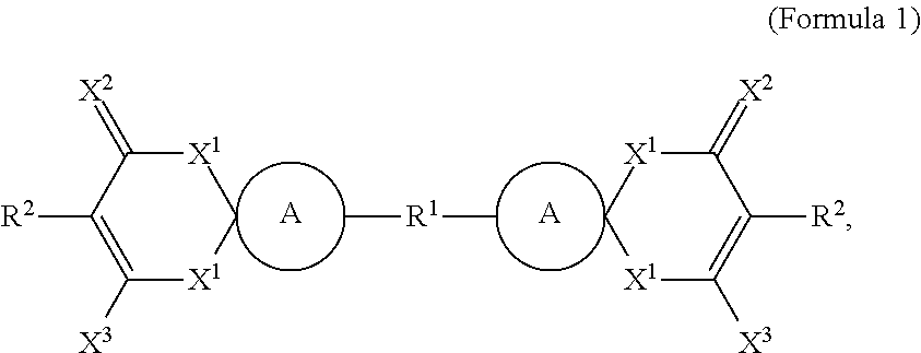
- the photoresist layer may have a chemical formula as shown in Formula 1.
- each A independently represents a substituted or a non-substituted cyclic alkyl group
- R 1 represents a CH 2 group, an oxygen atom, or a SO 2 group
- each R 2 independently represents a hydrogen atom, an azo group, or a substituted or a non-substituted polymethine group
- each X 1 independently represent an oxygen atom, a CH 2 group, an alkyl group, or an N—R 3 group, wherein R 3 represents a hydrogen atom, a substituted or a non-substituted C 1-18 alkyl group, a substituted or a non-substituted C 1-18 alkoxy group, a substituted or a non-substituted C 1-18 carboxyl group, a substituted or a non-substituted C 1-18 arylester group, an adamantyl carbonyl group, an adamantyl group, or a substituted or a non-substituted
- Formula 1 can be, but is not limited to, specific compounds as shown in Formula 1-1 to 1-25.
- the photoresist layer may have a chemical formula as shown in Formula 2 or 3.
- each B independently represents a substituted or a non-substituted aromatic hydrocarbon ring, a substituted or a non-substituted aromatic heterocyclic ring, or a substituted or a non-substituted condensed ring including an aromatic hydrocarbon ring; each R 4 independently represents a hydrogen atom, a C ⁇ S group, a substituted or non-substituted alkyl group, a substituted or non-substituted aryl group, a substituted or non-substituted aralkyl group, or a substituted or non-substituted heterocyclic group: each X 4 independently represents an oxygen atom, a substituted or non-substituted alkyl group, or an N—R 5 group, wherein R 5 represents a hydrogen atom, a substituted or a non-substituted C 1-18 alkyl group, a substituted or a non-substituted C 1-18 al
- Formula 2 can be, but is not limited to, specific compounds as shown in Formula 2-1 to 2-10.
- Formula 3 can be, but is not limited to, specific compounds as shown in Formula 3-1 to 3-9.
- the photoresist layer may have a chemical formula as shown in Formula 4.
- C represents a substituted or a non-substituted cyclic alkyl group
- each L independently represents a substituted or a non-substituted methine group
- each R 6 independently represents a substituted or a non-substituted C 1-18 alkyl group, a substituted or a non-substituted C 1-18 alkoxy group, a substituted or a non-substituted C 1-18 carboxyl group, a substituted or a non-substituted C 1-18 alkyl ester group, a substituted or a non-substituted arylester group, an adamantyl carbonyl group, an adamantyl group, or a substituted or a non-substituted aralkyl group
- each X 6 independently represents an oxygen atom, a CH 2 group, or an N—R′ group, wherein R 7 represents a substituted or a non-substituted C 1
- Formula 4 can be, but is not limited to, specific compounds as shown in Formula 4-1 to 4-3.
- the photoresist layer may have a chemical formula as shown in Formula 5.
- each L′ independently represent a substituted or a non-substituted methine group: each R 8 independently represents a hydrogen atom, a substituted or a non-substituted alkyl group, a substituted or a non-substituted aryl group, a substituted or a non-substituted aralkyl group, a substituted or a non-substituted heterocyclic ring, or a ferrocenyl group; R 9 represents a substituted or a non-substituted C 1-18 alkyl group, a substituted or a non-substituted C 1-18 alkoxy group, a substituted or a non-substituted C 1-18 carboxyl group, a substituted or a non-substituted C 1-18 alkyl ester group, a substituted or a non-substituted arylester group, an adamantyl carbonyl group, an adam
- Formula 5 can be, but is not limited to, specific compounds as shown in Formula 5-1 to 5-21.
- the photoresist layer may have a chemical formula as shown in Formula 6.
- each L′′ independently represent a substituted or a non-substituted methine group
- each R 11 independently represents a hydrogen atom, a substituted or a non-substituted alkyl group, a substituted or a non-substituted aryl group, a substituted or a non-substituted aralkyl group, or a substituted or a non-substituted heterocyclic ring
- R 12 represents a substituted or a non-substituted C 1-18 alkyl group, a substituted or a non-substituted C 1-18 alkoxy group, a substituted or a non-substituted C 1-18 carboxyl group, a substituted or a non-substituted C 1-18 alkyl ester group, a substituted or a non-substituted arylester group, an adamantyl carbonyl group, an adamantyl group, or a
- Formula 6 can be, but is not limited to, a specific compound as shown in Formula 6-1.
- the photoresist layer may have a chemical formula as shown in Formula 7.
- each L′ independently represent a substituted or a non-substituted methine group
- R 14 represents a substituted or a non-substituted C 1-18 alkyl group, a substituted or a non-substituted C 1-18 alkoxy group, a substituted or a non-substituted C 1-18 carboxyl group, a substituted or a non-substituted C 1-18 alkyl ester group, a substituted or a non-substituted arylester group, an adamantyl carbonyl group, an adamantyl group, or a substituted or a non-substituted aralkyl group
- each X 15 independently represents an oxygen atom, a sulfur atom, a CH 2 group, or an N—R 15 group, wherein R 15 represents a hydrogen atom or a substituted or a non-substituted C 1-18 alkyl group
- each X 16 independently represents an
- Formula 7 can be, but is not limited to, specific compounds as shown in Formula 7-1 to 7-3.
- the above photoresist material collocated with the focused laser beam has several advantages.
- the photoresist materials have high transparency and can be spin-coated on the layered material. Compared to the conventional PTM film, the photoresist materials of the disclosure have higher compatibility with existing equipment with a lower cost.
- the photoresist materials of the disclosure are spin-coated other than ultra-vacuum sputtered on the layered material. Contents of the photoresist materials of the disclosure are easily controlled to be coated on a large area substrate without a microscopic crystal phase/structure caused from the conventional PTM process.
- the photoresist layer thickness can be controlled by simple factors (e.g. rotation speed or concentration of the spin-on solution). As such, the photoresist layer of the disclosure has uniform thickness.
- the photoresist material of the disclosure is directly written on by the focused laser beam to process a heat chemistry surface relief reaction.
- the exposed pan of the photoresist material directly forms a groove or a pit without an additional development, thereby completing a patterned photoresist layer.
- the photoresist material of the disclosure is patterned by thermal chemistry (pyrolysis).
- thermal chemistry pyrolysis
- the conventional optical diffraction limit can be overcome, and the pattern resolution is therefore enhanced.
- the laser beam can be focused to a spot with a nano-scaled (less than 100 nm) diameter, e.g. of 30 nm to 60 nm.
- the photoresist material was spin coated on an aluminum nitride substrate to form a photoresist layer.
- the photoresist layer was patterned by a focused laser beam with a wavelength of 405 nm to form an opening for exposing the aluminum nitride substrate.
- the laser beam had a moving speed of 3 m/s and a power of 3.5 W (or 7 W).
- the exposed part of the aluminum nitride substrate was etched by reactive ion etching (RIE) to form a pore in the aluminum nitride substrate.
- the pore had a depth of 250 nm and a width of 450 nm to 500 nm.
- the RIE was processed with a chamber pressure of 30 mtorr, a process gas of BCl 3 /Ar (60 sccm/5 sccm), a plasma power of 300 W, and an etching period of 300 seconds.
- the photoresist materials, the photoresist layer thicknesses, the wavelength of maximum absorption in methanol of the photoresist materials, and the bottom opening widths (W) of the patterned photoresist layers were tabulated, respectively, and are shown in Table 1. Note that the pore in the substrate was broadened by the RIE factors. Those skilled in the an may adopt other anisotropic etching processes or factors to match the pore width and the bottom opening width of the patterned photoresist layer.
- Photoresist Wavelength of Bottom opening width Photoresist layer maximum absorption of the patterned material thickness (in methanol) photoresist layer Formula 1-8 464 nm Formula 1-13 453 nm Formula 1-17 432 nm Formula 1-19 391 nm Formula 1-23 377 nm Formula 2-1 396 nm Formula 2-2 381 nm Formula 2-10 435 nm Formula 3-1 50 nm 381 nm 97 nm Formula 3-2 379 nm Formula 3-3 395 nm Formula 3-4 394 nm Formula 3-9 435 nm Formula 4-1 478 nm Formula 4-2 458 nm Formula 5-2 100 nm 452 nm 231 nm Formula 5-15 450 nm Formula 5-18 100 nm 489 nm 350 nm Formula 5-21 459 nm Formula 5-21 431 nm Formula 7-1 100 nm 477 nm 260 nm Formula 7-2 497 nm Formula 7-3 511
Landscapes
- Engineering & Computer Science (AREA)
- Physics & Mathematics (AREA)
- Chemical & Material Sciences (AREA)
- Nanotechnology (AREA)
- General Physics & Mathematics (AREA)
- Crystallography & Structural Chemistry (AREA)
- Spectroscopy & Molecular Physics (AREA)
- Mathematical Physics (AREA)
- Theoretical Computer Science (AREA)
- Organic Chemistry (AREA)
- Condensed Matter Physics & Semiconductors (AREA)
- Manufacturing & Machinery (AREA)
- Materials For Photolithography (AREA)
- Exposure And Positioning Against Photoresist Photosensitive Materials (AREA)
Abstract
Description

wherein: each A independently represents a substituted or a non-substituted cyclic alkyl group; R1 represents a CH2 group, an oxygen atom, or a SO2 group; each R2 independently represents a hydrogen atom, an azo group, or a substituted or a non-substituted polymethine group; each X1 independently represent an oxygen atom, a CH2 group, an alkyl group, or an N—R3 group, wherein R3 represents a hydrogen atom, a substituted or a non-substituted C1-18 alkyl group, a substituted or a non-substituted C1-18 alkoxy group, a substituted or a non-substituted C1-18 carboxyl group, a substituted or a non-substituted C1-18 arylester group, an adamantyl carbonyl group, an adamantyl group, or a substituted or a non-substituted aralkyl group; each X2 independently represents an oxygen atom or a C(CN)2 group; and each X3 independently represents an oxygen atom posing one negative charge, a hydroxyl group, or a C(CN)2 group;

wherein each B independently represents a substituted or a non-substituted aromatic hydrocarbon ring, a substituted or a non-substituted aromatic heterocyclic ring, or a substituted or a non-substituted condensed ring including an aromatic hydrocarbon ring; each R4 independently represents a hydrogen atom, a C═S group, a substituted or non-substituted alkyl group, a substituted or non-substituted aryl group, a substituted or non-substituted aralkyl group, or a substituted or non-substituted heterocyclic group; each X4 independently represents an oxygen atom, a substituted or non-substituted alkyl group, or an N—R5 group, wherein R5 represents a hydrogen atom, a substituted or a non-substituted C1-18 alkyl group, a substituted or a non-substituted C1-18 alkoxy group, a substituted or a non-substituted C1-18 carboxyl group, a substituted or a non-substituted C1-18 alkyl ester group, a substituted or a non-substituted arylester group, an adamantyl carbonyl group, an adamantyl group, or a substituted or a non-substituted aralkyl group; each R5 independently represents an oxygen atom, a C(CN)2 group, or a C═O group; and M represents Fe, Co, Cu, Ni, or Zn;

wherein C represents a substituted or a non-substituted cyclic alkyl group; each L independently represents a substituted or a non-substituted methine group; each R6 independently represents a substituted or a non-substituted C1-18 alkyl group, a substituted or a non-substituted C1-18 alkoxy group, a substituted or a non-substituted C1-18 carboxyl group, a substituted or a non-substituted C1-18 alkyl ester group, a substituted or a non-substituted arylester group, an adamantyl carbonyl group, an adamantyl group, or a substituted or a non-substituted aralkyl group; each X6 independently represents an oxygen atom, a CH2 group, or an N—R7 group, wherein R7 represents a substituted or a non-substituted C1-18 alkyl group; each X7 independently represents an oxygen atom or a C(CN)2 group; each X8 independently represents a substituted or a non-substituted alkylene group, or an a substituted or a non-substituted alkylene group containing an oxygen atom, a sulfur atom, a selenium atom, or a nitrogen atom; and each m independently represents an integer of 0 or 1;

wherein each L′ independently represent a substituted or a non-substituted methine group; each R8 independently represents a hydrogen atom, a substituted or a non-substituted alkyl group, a substituted or a non-substituted aryl group, a substituted or a non-substituted aralkyl group, a substituted or a non-substituted heterocyclic ring, or a ferrocenyl group: R9 represents a substituted or a non-substituted C1-18 alkyl group, a substituted or a non-substituted C1-18 alkoxy group, a substituted or a non-substituted C1-18 carboxyl group, a substituted or a non-substituted C1-18 alkyl ester group, a substituted or a non-substituted arylester group, an adamantyl carbonyl group, an adamantyl group, or a substituted or a non-substituted aralkyl group; each X9 independently represents an oxygen atom, a CH2 group, or an N—R10 group, herein R10 represents a substituted or a non-substituted C1-18 alkyl group; each X10 independently represents an oxygen atom or a C(CN)2 group; X11 represents a substituted or a non-substituted alkylene group, or a substituted or a non-substituted alkylene group containing an oxygen atom, a sulfur atom, a selenium atom, or a nitrogen atom; and n is an integer of 0 or 1;

wherein each L″ independently represent a substituted or a non-substituted methine group; each R11 independently represents a hydrogen atom, a substituted or a non-substituted alkyl group, a substituted or a non-substituted aryl group, a substituted or a non-substituted aralkyl group, or a substituted or a non-substituted heterocyclic ring; R12 represents a substituted or a non-substituted C1-18 alkyl group, a substituted or a non-substituted C1-18 alkoxy group, a substituted or a non-substituted C1-18 carboxyl group, a substituted or a non-substituted C1-18 alkyl ester group, a substituted or a non-substituted arylester group, an adamantyl carbonyl group, an adamantyl group, or a substituted or a non-substituted aralkyl group; each X12 independently represents an oxygen atom, a CH2 group, or an N—R13 group, wherein R13 represents a substituted or a non-substituted C1-18 alkyl group; each X13 independently represents an oxygen atom or a C(CN)2 group; each X14 independently represents a substituted or a non-substituted alkylene group, or a substituted or a non-substituted alkylene group containing an oxygen atom, a sulfur atom, a selenium atom, or a nitrogen atom; and each k independently represents an integer of 0 or 1;

wherein each L′ independently represent a substituted or a non-substituted methine group; R14 represents a substituted or a non-substituted C1-18 alkyl group, a substituted or a non-substituted C1-18 alkoxy group, a substituted or a non-substituted C1-18 carboxyl group, a substituted or a non-substituted C1-18 alkyl ester group, a substituted or a non-substituted arylester group, an adamantyl carbonyl group, an adamantyl group, or a substituted or a non-substituted aralkyl group: each X15 independently represents an oxygen atom, a sulfur atom, a CH2 group, or an N—R15 group, wherein R15 represents a hydrogen atom or a substituted or a non-substituted C1-18 alkyl group; each X17 independently represents an oxygen atom, a sulfur atom, or a C(CN)2 group; X17 represents a substituted or a non-substituted alkylene group, or a substituted or a non-substituted alkylene group containing an oxygen atom, a sulfur atom, a selenium atom, or a nitrogen atom; and n is an integer of 0 or 1.
wherein each A independently represents a substituted or a non-substituted cyclic alkyl group; R1 represents a CH2 group, an oxygen atom, or a SO2 group; each R2 independently represents a hydrogen atom, an azo group, or a substituted or a non-substituted polymethine group; each X1 independently represent an oxygen atom, a CH2 group, an alkyl group, or an N—R3 group, wherein R3 represents a hydrogen atom, a substituted or a non-substituted C1-18 alkyl group, a substituted or a non-substituted C1-18 alkoxy group, a substituted or a non-substituted C1-18 carboxyl group, a substituted or a non-substituted C1-18 arylester group, an adamantyl carbonyl group, an adamantyl group, or a substituted or a non-substituted aralkyl group; each X2 independently represents an oxygen atom or a C(CN)2 group; and each X3 independently represents an oxygen atom posing one negative charge, a hydroxyl group, or a C(CN)2 group;

wherein each B independently represents a substituted or a non-substituted aromatic hydrocarbon ring, a substituted or a non-substituted aromatic heterocyclic ring, or a substituted or a non-substituted condensed ring including an aromatic hydrocarbon ring; each R4 independently represents a hydrogen atom, a C═S group, a substituted or non-substituted alkyl group, a substituted or non-substituted aryl group, a substituted or non-substituted aralkyl group, or a substituted or non-substituted heterocyclic group; each X4 independently represents an oxygen atom, a substituted or non-substituted alkyl group, or an N—R5 group, wherein R5 represents a hydrogen atom, a substituted or a non-substituted C1-18, alkyl group, a substituted or a non-substituted C1-18 alkoxy group, a substituted or a non-substituted C1-18 carboxyl group, a substituted or a non-substituted C1-18 alkyl ester group, a substituted or a non-substituted arylester group, an adamantyl carbonyl group, an adamantyl group, or a substituted or a non-substituted aralkyl group; each R5 independently represents an oxygen atom, a C(CN)2 group, or a C═O group; and M represents Fe, Co, Cu, Ni, or Zn;

wherein C represents a substituted or a non-substituted cyclic alkyl group; each L independently represents a substituted or a non-substituted methine group; each R6 independently represents a substituted or a non-substituted C1-18 alkyl group, a substituted or a non-substituted C1-18 alkoxy group, a substituted or a non-substituted C1-18 carboxyl group, a substituted or a non-substituted C1-18 alkyl ester group, a substituted or a non-substituted arylester group, an adamantyl carbonyl group, an adamantyl group, or a substituted or a non-substituted aralkyl group; each X6 independently represents an oxygen atom, a CH2 group, or an N—R7 group, wherein R7 represents a substituted or a non-substituted C1-18 alkyl group; each X7 independently represents an oxygen atom or a C(CN)2 group; each X8 independently represents a substituted or a non-substituted alkylene group, or an a substituted or a non-substituted alkylene group containing an oxygen atom, a sulfur atom, a selenium atom, or a nitrogen atom; and each m independently represents an integer of 0 or 1;

wherein each L′ independently represent a substituted or a non-substituted methine group; each R8 independently represents a hydrogen atom, a substituted or a non-substituted alkyl group, a substituted or a non-substituted aryl group, a substituted or a non-substituted aralkyl group, a substituted or a non-substituted heterocyclic ring, or a ferrocenyl group; R9 represents a substituted or a non-substituted C1-18 alkyl group, a substituted or a non-substituted C1-18 alkoxy group, a substituted or a non-substituted C1-18 carboxyl group, a substituted or a non-substituted C1-18 alkyl ester group, a substituted or a non-substituted arylester group, an adamantyl carbonyl group, an adamantyl group, or a substituted or a non-substituted aralkyl group; each X9 independently represents an oxygen atom, a CH2 group, or an N—R10 group, wherein R10 represents a substituted or a non-substituted C1-18 alkyl group; each X10 independently represents an oxygen atom or a C(CN)2 group; X11 represents a substituted or a non-substituted alkylene group, or a substituted or a non-substituted alkylene group containing an oxygen atom, a sulfur atom, a selenium atom, or a nitrogen atom; and n is an integer of 0 or 1;

wherein each L″ independently represent a substituted or a non-substituted methine group; each R11 independently represents a hydrogen atom, a substituted or a non-substituted alkyl group, a substituted or a non-substituted aryl group, a substituted or a non-substituted aralkyl group, or a substituted or a non-substituted heterocyclic ring; R12 represents a substituted or a non-substituted C1-18 alkyl group, a substituted or a non-substituted C1-18 alkoxy group, a substituted or a non-substituted C1-18 carboxyl group, a substituted or a non-substituted C1-18 alkyl ester group, a substituted or a non-substituted arylester group, an adamantyl carbonyl group, an adamantyl group, or a substituted or a non-substituted aralkyl group; each X12 independently represents an oxygen atom, a CH2 group, or an N—R13 group, wherein R13 represents a substituted or a non-substituted C1-18 alkyl group; each X13 independently represents an oxygen atom or a C(CN)2 group; each X14 independently represents a substituted or a non-substituted alkylene group, or a substituted or a non-substituted alkylene group containing an oxygen atom, a sulfur atom, a selenium atom, or a nitrogen atom; and each k independently represents an integer of 0 or 1;

wherein each L′ independently represent a substituted or a non-substituted methine group; R14 represents a substituted or a non-substituted C1-18 alkyl group, a substituted or a non-substituted C1-18 alkoxy group, a substituted or a non-substituted C1-18 carboxyl group, a substituted or a non-substituted C1-18 alkyl ester group, a substituted or a non-substituted arylester group, an adamantyl carbonyl group, an adamantyl group, or a substituted or a non-substituted aralkyl group: each X15 independently represents an oxygen atom, a sulfur atom, a CH2 group, or an N—R15 group, wherein R15 represents a hydrogen atom or a substituted or a non-substituted C1-18 alkyl group; each X16 independently represents an oxygen atom, a sulfur atom, or a C(CN)2 group; X17 represents a substituted or a non-substituted alkylene group, or a substituted or a non-substituted alkylene group containing an oxygen atom, a sulfur atom, a selenium atom, or a nitrogen atom; and n is an integer of 0 or 1.


| TABLE 1 | |||
| Photoresist | Wavelength of | Bottom opening width | |
| Photoresist | layer | maximum absorption | of the patterned |
| material | thickness | (in methanol) | photoresist layer |
| Formula 1-8 | 464 nm | ||
| Formula 1-13 | 453 nm | ||
| Formula 1-17 | 432 nm | ||
| Formula 1-19 | 391 nm | ||
| Formula 1-23 | 377 nm | ||
| Formula 2-1 | 396 nm | ||
| Formula 2-2 | 381 nm | ||
| Formula 2-10 | 435 nm | ||
| Formula 3-1 | 50 nm | 381 nm | 97 nm |
| Formula 3-2 | 379 nm | ||
| Formula 3-3 | 395 nm | ||
| Formula 3-4 | 394 nm | ||
| Formula 3-9 | 435 nm | ||
| Formula 4-1 | 478 nm | ||
| Formula 4-2 | 458 nm | ||
| Formula 5-2 | 100 nm | 452 nm | 231 nm |
| Formula 5-15 | 450 nm | ||
| Formula 5-18 | 100 nm | 489 nm | 350 nm |
| Formula 5-21 | 459 nm | ||
| Formula 5-21 | 431 nm | ||
| Formula 7-1 | 100 nm | 477 nm | 260 nm |
| Formula 7-2 | 497 nm | ||
| Formula 7-3 | 511 nm | ||
Claims (14)


Applications Claiming Priority (3)
| Application Number | Priority Date | Filing Date | Title |
|---|---|---|---|
| TW101109443 | 2012-03-20 | ||
| TW101109443A | 2012-03-20 | ||
| TW101109443A TW201339744A (en) | 2012-03-20 | 2012-03-20 | Methods of patterning layered-material and forming imprinting mold |
Publications (2)
| Publication Number | Publication Date |
|---|---|
| US8540888B1 true US8540888B1 (en) | 2013-09-24 |
| US20130248482A1 US20130248482A1 (en) | 2013-09-26 |
Family
ID=49181432
Family Applications (1)
| Application Number | Title | Priority Date | Filing Date |
|---|---|---|---|
| US13/609,854 Expired - Fee Related US8540888B1 (en) | 2012-03-20 | 2012-09-11 | Methods of patterning layered-material and forming imprinting mold |
Country Status (3)
| Country | Link |
|---|---|
| US (1) | US8540888B1 (en) |
| CN (1) | CN103324026A (en) |
| TW (1) | TW201339744A (en) |
Cited By (3)
| Publication number | Priority date | Publication date | Assignee | Title |
|---|---|---|---|---|
| US10662058B1 (en) | 2019-03-05 | 2020-05-26 | Rosemount Aerospace Inc. | Wet etch patterning of an aluminum nitride film |
| US11104043B2 (en) * | 2017-07-13 | 2021-08-31 | Dalian University Of Technology | Thermal extrusion method to fabricate large-dimension superhydrophobic cylinder pillar arrays with droplet pancake bouncing phenomenon |
| WO2022176778A1 (en) * | 2021-02-16 | 2022-08-25 | 富士フイルム株式会社 | Curable composition for imprinting, cured product, imprinting pattern production method, and device manufacturing method |
Families Citing this family (1)
| Publication number | Priority date | Publication date | Assignee | Title |
|---|---|---|---|---|
| TWI755723B (en) * | 2020-05-05 | 2022-02-21 | 力晶積成電子製造股份有限公司 | Patterning method |
Citations (7)
| Publication number | Priority date | Publication date | Assignee | Title |
|---|---|---|---|---|
| US5814431A (en) * | 1996-01-10 | 1998-09-29 | Mitsubishi Chemical Corporation | Photosensitive composition and lithographic printing plate |
| US6355396B1 (en) * | 1999-03-25 | 2002-03-12 | Fuji Photo Film Co., Ltd. | Photosensitive composition and planographic printing plate precursor using same |
| WO2006045332A1 (en) | 2004-10-27 | 2006-05-04 | Singulus Mastering B.V. | Mastering process with phase-change materials |
| US7465530B1 (en) | 2007-08-16 | 2008-12-16 | Industrial Technology Research Institute | Inorganic resist material and nano-fabrication method by utilizing the same |
| US20100112491A1 (en) | 2002-10-10 | 2010-05-06 | Sony Corporation | Method for manufacturing optical disc master and method for manufacturing optical disc |
| US7741006B2 (en) | 2007-02-02 | 2010-06-22 | Industrial Technology Research Institute | Laser patterning method for fabricating disc stamper |
| US7741004B2 (en) | 2006-12-27 | 2010-06-22 | Industrial Technology Research Institute | Method of forming pattern by utilizing coatable inorganic material |
Family Cites Families (3)
| Publication number | Priority date | Publication date | Assignee | Title |
|---|---|---|---|---|
| US7781044B2 (en) * | 2007-09-05 | 2010-08-24 | Industrial Technology Research Institute | Organic compound for recording layer for high speed recording of information and optical recording medium including the same |
| US20090087620A1 (en) * | 2007-09-29 | 2009-04-02 | Industrial Technology Research Institute | Organic compounds for recording layer for recording of information and optical recording medium including the same |
| CN102320553B (en) * | 2011-07-04 | 2014-11-26 | 中国科学院理化技术研究所 | Method for manufacturing micro-nano structure device by using laser two-photon direct writing technology |
-
2012
- 2012-03-20 TW TW101109443A patent/TW201339744A/en unknown
- 2012-09-11 US US13/609,854 patent/US8540888B1/en not_active Expired - Fee Related
- 2012-10-10 CN CN2012103828541A patent/CN103324026A/en active Pending
Patent Citations (7)
| Publication number | Priority date | Publication date | Assignee | Title |
|---|---|---|---|---|
| US5814431A (en) * | 1996-01-10 | 1998-09-29 | Mitsubishi Chemical Corporation | Photosensitive composition and lithographic printing plate |
| US6355396B1 (en) * | 1999-03-25 | 2002-03-12 | Fuji Photo Film Co., Ltd. | Photosensitive composition and planographic printing plate precursor using same |
| US20100112491A1 (en) | 2002-10-10 | 2010-05-06 | Sony Corporation | Method for manufacturing optical disc master and method for manufacturing optical disc |
| WO2006045332A1 (en) | 2004-10-27 | 2006-05-04 | Singulus Mastering B.V. | Mastering process with phase-change materials |
| US7741004B2 (en) | 2006-12-27 | 2010-06-22 | Industrial Technology Research Institute | Method of forming pattern by utilizing coatable inorganic material |
| US7741006B2 (en) | 2007-02-02 | 2010-06-22 | Industrial Technology Research Institute | Laser patterning method for fabricating disc stamper |
| US7465530B1 (en) | 2007-08-16 | 2008-12-16 | Industrial Technology Research Institute | Inorganic resist material and nano-fabrication method by utilizing the same |
Non-Patent Citations (4)
| Title |
|---|
| Chin-Tien Yang, Chih-Yu Chen, Chun-Chieh Huang, Yuan-Chin Lee, Shuen-Chen Chen, and Chung-Ta Cheng "Single Wavelength Blue-Laser Optical Head-Like Opto-Mechanical System for Turntable Thermal Mode Lithography and Stamper Fabrication", Magnetics, IEEE Transactions on vol. 47 , No. 3, Mar. 2011, pp. 701-705. |
| Chin-Tien Yang, Ming-Fang Hsu, Sheng Li Chang, Jung-Po Chen, Tzuan-Ren Jeng, and Kuo-Chi Chiu "Spin Coatable Inorganic Resist for High Density Disk Mastering Process Application", Japanese Journal of Applied Physics, vol. 47, 2008, pp. 6023-6024. |
| Yoshihisa Usami, Tetsuya Watanabe, Yoshinori Kanazawa, Kazuaki Taga, Hiroshi Kawai, and Kimio Ichikawa "405nm Laser Thermal Lithography of 40 nm Pattern Using Super Resolution Organic Resist Material", Applied Physics Express 2, published online Nov. 27, 2009, pp. 126502-1-126502-3, No. 7. |
| Yu-Hsuan Lin, Chih-Chung Yang, Chin-Tien Yang, Shi-Wei Chen, Chin-Ming Chu, and Donyau Chiang, "Deep Dry Etching Patterned Silicon Using GeSbSnOx Thermal Lithography Photoresist", Magnetics, IEEE Transactions on vol. 47 , No. 3, Mar. 2011, pp. 560-563. |
Cited By (4)
| Publication number | Priority date | Publication date | Assignee | Title |
|---|---|---|---|---|
| US11104043B2 (en) * | 2017-07-13 | 2021-08-31 | Dalian University Of Technology | Thermal extrusion method to fabricate large-dimension superhydrophobic cylinder pillar arrays with droplet pancake bouncing phenomenon |
| US10662058B1 (en) | 2019-03-05 | 2020-05-26 | Rosemount Aerospace Inc. | Wet etch patterning of an aluminum nitride film |
| WO2022176778A1 (en) * | 2021-02-16 | 2022-08-25 | 富士フイルム株式会社 | Curable composition for imprinting, cured product, imprinting pattern production method, and device manufacturing method |
| JPWO2022176778A1 (en) * | 2021-02-16 | 2022-08-25 |
Also Published As
| Publication number | Publication date |
|---|---|
| CN103324026A (en) | 2013-09-25 |
| US20130248482A1 (en) | 2013-09-26 |
| TW201339744A (en) | 2013-10-01 |
Similar Documents
| Publication | Publication Date | Title |
|---|---|---|
| US8540888B1 (en) | Methods of patterning layered-material and forming imprinting mold | |
| CN106030406B (en) | Method for uniform imprint pattern transfer of sub-20 nm features | |
| TWI335033B (en) | Laser beam directed pattern formation for disc stamper creation | |
| JP2006110434A (en) | Pattern forming method and structure processing method using the same | |
| JP5814868B2 (en) | Method for manufacturing magnetic recording medium | |
| CN107255905A (en) | Dry-etching thermal-reactive anticorrosive additive material, the manufacture method of mould and mould | |
| TWI430467B (en) | Solar battery with an anti-reflect surface and the manufacturing method thereof | |
| JP2015011746A (en) | Pattern formation method, magnetic recording medium manufacturing method using the same, magnetic recording medium, and stamper manufacturing method | |
| TW200910343A (en) | Inorganic resist material and nano-fabrication method by utilizing the same | |
| US9156216B2 (en) | Process for manufacturing a segmented optical structure | |
| CN102566259A (en) | Methods of Forming Nanostructures | |
| JP2013171596A (en) | Magnetic recording medium and method for manufacturing the same | |
| EP1429323A3 (en) | Optical recording medium with phase transition layer and method of manufacturing the optical recording medium | |
| JP2007193249A (en) | Manufacturing method of molded parts | |
| CN100390886C (en) | Method for manufacturing master disc for optical information recording medium, disc of the master disc | |
| US20100119778A1 (en) | Ultra thin alignment walls for di-block copolymer | |
| CN102043330A (en) | Method for manufacturing roller mold core for nano imprinting | |
| CN103681249B (en) | The preparation method of delicate pattern of semi-conductor device | |
| TWI326001B (en) | Coatable inorganic material and method of forming pattern by utilizing the same | |
| CN112114391A (en) | A kind of plasmon absorber and preparation method thereof | |
| JP2005283814A (en) | Optical element subjected to antireflection treatment, mold thereof and method of manufacturing mold | |
| CN103376484A (en) | Method for producing grating by employing Lift-Off principle | |
| CN101286004B (en) | An inorganic thermal resistance film for photolithography | |
| WO2013024635A1 (en) | Patterned media and method for producing same | |
| TWI337756B (en) | Method of manufacturing an imprinting template utilizing a semiconductor manufacturing process and the imprinting template obtained |
Legal Events
| Date | Code | Title | Description |
|---|---|---|---|
| AS | Assignment |
Owner name: INDUSTRIAL TECHNOLOGY RESEARCH INSTITUTE, TAIWAN Free format text: ASSIGNMENT OF ASSIGNORS INTEREST;ASSIGNORS:YANG, CHIN-TIEN;LI, MING-CHIA;CHENG, CHUNG-TA;REEL/FRAME:029011/0371 Effective date: 20120904 |
|
| STCF | Information on status: patent grant |
Free format text: PATENTED CASE |
|
| FPAY | Fee payment |
Year of fee payment: 4 |
|
| MAFP | Maintenance fee payment |
Free format text: PAYMENT OF MAINTENANCE FEE, 8TH YEAR, LARGE ENTITY (ORIGINAL EVENT CODE: M1552); ENTITY STATUS OF PATENT OWNER: LARGE ENTITY Year of fee payment: 8 |
|
| FEPP | Fee payment procedure |
Free format text: MAINTENANCE FEE REMINDER MAILED (ORIGINAL EVENT CODE: REM.); ENTITY STATUS OF PATENT OWNER: LARGE ENTITY |
|
| LAPS | Lapse for failure to pay maintenance fees |
Free format text: PATENT EXPIRED FOR FAILURE TO PAY MAINTENANCE FEES (ORIGINAL EVENT CODE: EXP.); ENTITY STATUS OF PATENT OWNER: LARGE ENTITY |
|
| STCH | Information on status: patent discontinuation |
Free format text: PATENT EXPIRED DUE TO NONPAYMENT OF MAINTENANCE FEES UNDER 37 CFR 1.362 |
|
| FP | Lapsed due to failure to pay maintenance fee |
Effective date: 20250924 |