US8535959B2 - Method for producing large lighting with power LED - Google Patents
Method for producing large lighting with power LED Download PDFInfo
- Publication number
- US8535959B2 US8535959B2 US13/512,328 US201013512328A US8535959B2 US 8535959 B2 US8535959 B2 US 8535959B2 US 201013512328 A US201013512328 A US 201013512328A US 8535959 B2 US8535959 B2 US 8535959B2
- Authority
- US
- United States
- Prior art keywords
- power led
- heat radiation
- pcb
- lighting
- hole
- Prior art date
- Legal status (The legal status is an assumption and is not a legal conclusion. Google has not performed a legal analysis and makes no representation as to the accuracy of the status listed.)
- Expired - Fee Related
Links
Images


Classifications
-
- H—ELECTRICITY
- H10—SEMICONDUCTOR DEVICES; ELECTRIC SOLID-STATE DEVICES NOT OTHERWISE PROVIDED FOR
- H10H—INORGANIC LIGHT-EMITTING SEMICONDUCTOR DEVICES HAVING POTENTIAL BARRIERS
- H10H20/00—Individual inorganic light-emitting semiconductor devices having potential barriers, e.g. light-emitting diodes [LED]
- H10H20/80—Constructional details
- H10H20/85—Packages
- H10H20/858—Means for heat extraction or cooling
- H10H20/8585—Means for heat extraction or cooling being an interconnection
-
- F—MECHANICAL ENGINEERING; LIGHTING; HEATING; WEAPONS; BLASTING
- F21—LIGHTING
- F21K—NON-ELECTRIC LIGHT SOURCES USING LUMINESCENCE; LIGHT SOURCES USING ELECTROCHEMILUMINESCENCE; LIGHT SOURCES USING CHARGES OF COMBUSTIBLE MATERIAL; LIGHT SOURCES USING SEMICONDUCTOR DEVICES AS LIGHT-GENERATING ELEMENTS; LIGHT SOURCES NOT OTHERWISE PROVIDED FOR
- F21K9/00—Light sources using semiconductor devices as light-generating elements, e.g. using light-emitting diodes [LED] or lasers
- F21K9/90—Methods of manufacture
-
- F—MECHANICAL ENGINEERING; LIGHTING; HEATING; WEAPONS; BLASTING
- F21—LIGHTING
- F21V—FUNCTIONAL FEATURES OR DETAILS OF LIGHTING DEVICES OR SYSTEMS THEREOF; STRUCTURAL COMBINATIONS OF LIGHTING DEVICES WITH OTHER ARTICLES, NOT OTHERWISE PROVIDED FOR
- F21V29/00—Protecting lighting devices from thermal damage; Cooling or heating arrangements specially adapted for lighting devices or systems
- F21V29/50—Cooling arrangements
- F21V29/70—Cooling arrangements characterised by passive heat-dissipating elements, e.g. heat-sinks
-
- F—MECHANICAL ENGINEERING; LIGHTING; HEATING; WEAPONS; BLASTING
- F21—LIGHTING
- F21V—FUNCTIONAL FEATURES OR DETAILS OF LIGHTING DEVICES OR SYSTEMS THEREOF; STRUCTURAL COMBINATIONS OF LIGHTING DEVICES WITH OTHER ARTICLES, NOT OTHERWISE PROVIDED FOR
- F21V29/00—Protecting lighting devices from thermal damage; Cooling or heating arrangements specially adapted for lighting devices or systems
- F21V29/85—Protecting lighting devices from thermal damage; Cooling or heating arrangements specially adapted for lighting devices or systems characterised by the material
- F21V29/89—Metals
-
- H—ELECTRICITY
- H05—ELECTRIC TECHNIQUES NOT OTHERWISE PROVIDED FOR
- H05K—PRINTED CIRCUITS; CASINGS OR CONSTRUCTIONAL DETAILS OF ELECTRIC APPARATUS; MANUFACTURE OF ASSEMBLAGES OF ELECTRICAL COMPONENTS
- H05K1/00—Printed circuits
- H05K1/02—Details
- H05K1/0201—Thermal arrangements, e.g. for cooling, heating or preventing overheating
- H05K1/0203—Cooling of mounted components
- H05K1/0204—Cooling of mounted components using means for thermal conduction connection in the thickness direction of the substrate
- H05K1/0206—Cooling of mounted components using means for thermal conduction connection in the thickness direction of the substrate by printed thermal vias
-
- H—ELECTRICITY
- H10—SEMICONDUCTOR DEVICES; ELECTRIC SOLID-STATE DEVICES NOT OTHERWISE PROVIDED FOR
- H10H—INORGANIC LIGHT-EMITTING SEMICONDUCTOR DEVICES HAVING POTENTIAL BARRIERS
- H10H20/00—Individual inorganic light-emitting semiconductor devices having potential barriers, e.g. light-emitting diodes [LED]
- H10H20/80—Constructional details
- H10H20/85—Packages
- H10H20/858—Means for heat extraction or cooling
- H10H20/8582—Means for heat extraction or cooling characterised by their shape
-
- F—MECHANICAL ENGINEERING; LIGHTING; HEATING; WEAPONS; BLASTING
- F21—LIGHTING
- F21K—NON-ELECTRIC LIGHT SOURCES USING LUMINESCENCE; LIGHT SOURCES USING ELECTROCHEMILUMINESCENCE; LIGHT SOURCES USING CHARGES OF COMBUSTIBLE MATERIAL; LIGHT SOURCES USING SEMICONDUCTOR DEVICES AS LIGHT-GENERATING ELEMENTS; LIGHT SOURCES NOT OTHERWISE PROVIDED FOR
- F21K9/00—Light sources using semiconductor devices as light-generating elements, e.g. using light-emitting diodes [LED] or lasers
-
- F—MECHANICAL ENGINEERING; LIGHTING; HEATING; WEAPONS; BLASTING
- F21—LIGHTING
- F21W—INDEXING SCHEME ASSOCIATED WITH SUBCLASSES F21K, F21L, F21S and F21V, RELATING TO USES OR APPLICATIONS OF LIGHTING DEVICES OR SYSTEMS
- F21W2131/00—Use or application of lighting devices or systems not provided for in codes F21W2102/00-F21W2121/00
- F21W2131/10—Outdoor lighting
- F21W2131/103—Outdoor lighting of streets or roads
-
- F—MECHANICAL ENGINEERING; LIGHTING; HEATING; WEAPONS; BLASTING
- F21—LIGHTING
- F21Y—INDEXING SCHEME ASSOCIATED WITH SUBCLASSES F21K, F21L, F21S and F21V, RELATING TO THE FORM OR THE KIND OF THE LIGHT SOURCES OR OF THE COLOUR OF THE LIGHT EMITTED
- F21Y2115/00—Light-generating elements of semiconductor light sources
- F21Y2115/10—Light-emitting diodes [LED]
-
- H—ELECTRICITY
- H05—ELECTRIC TECHNIQUES NOT OTHERWISE PROVIDED FOR
- H05K—PRINTED CIRCUITS; CASINGS OR CONSTRUCTIONAL DETAILS OF ELECTRIC APPARATUS; MANUFACTURE OF ASSEMBLAGES OF ELECTRICAL COMPONENTS
- H05K2201/00—Indexing scheme relating to printed circuits covered by H05K1/00
- H05K2201/03—Conductive materials
- H05K2201/0302—Properties and characteristics in general
- H05K2201/0305—Solder used for other purposes than connections between PCB or components, e.g. for filling vias or for programmable patterns
-
- H—ELECTRICITY
- H05—ELECTRIC TECHNIQUES NOT OTHERWISE PROVIDED FOR
- H05K—PRINTED CIRCUITS; CASINGS OR CONSTRUCTIONAL DETAILS OF ELECTRIC APPARATUS; MANUFACTURE OF ASSEMBLAGES OF ELECTRICAL COMPONENTS
- H05K2201/00—Indexing scheme relating to printed circuits covered by H05K1/00
- H05K2201/09—Shape and layout
- H05K2201/09818—Shape or layout details not covered by a single group of H05K2201/09009 - H05K2201/09809
- H05K2201/09854—Hole or via having special cross-section, e.g. elliptical
-
- H—ELECTRICITY
- H05—ELECTRIC TECHNIQUES NOT OTHERWISE PROVIDED FOR
- H05K—PRINTED CIRCUITS; CASINGS OR CONSTRUCTIONAL DETAILS OF ELECTRIC APPARATUS; MANUFACTURE OF ASSEMBLAGES OF ELECTRICAL COMPONENTS
- H05K2201/00—Indexing scheme relating to printed circuits covered by H05K1/00
- H05K2201/10—Details of components or other objects attached to or integrated in a printed circuit board
- H05K2201/10007—Types of components
- H05K2201/10106—Light emitting diode [LED]
-
- H—ELECTRICITY
- H05—ELECTRIC TECHNIQUES NOT OTHERWISE PROVIDED FOR
- H05K—PRINTED CIRCUITS; CASINGS OR CONSTRUCTIONAL DETAILS OF ELECTRIC APPARATUS; MANUFACTURE OF ASSEMBLAGES OF ELECTRICAL COMPONENTS
- H05K2203/00—Indexing scheme relating to apparatus or processes for manufacturing printed circuits covered by H05K3/00
- H05K2203/15—Position of the PCB during processing
- H05K2203/1572—Processing both sides of a PCB by the same process; Providing a similar arrangement of components on both sides; Making interlayer connections from two sides
-
- H—ELECTRICITY
- H05—ELECTRIC TECHNIQUES NOT OTHERWISE PROVIDED FOR
- H05K—PRINTED CIRCUITS; CASINGS OR CONSTRUCTIONAL DETAILS OF ELECTRIC APPARATUS; MANUFACTURE OF ASSEMBLAGES OF ELECTRICAL COMPONENTS
- H05K3/00—Apparatus or processes for manufacturing printed circuits
- H05K3/0011—Working of insulating substrates or insulating layers
- H05K3/0044—Mechanical working of the substrate, e.g. drilling or punching
- H05K3/0047—Drilling of holes
-
- H—ELECTRICITY
- H05—ELECTRIC TECHNIQUES NOT OTHERWISE PROVIDED FOR
- H05K—PRINTED CIRCUITS; CASINGS OR CONSTRUCTIONAL DETAILS OF ELECTRIC APPARATUS; MANUFACTURE OF ASSEMBLAGES OF ELECTRICAL COMPONENTS
- H05K3/00—Apparatus or processes for manufacturing printed circuits
- H05K3/0058—Laminating printed circuit boards onto other substrates, e.g. metallic substrates
- H05K3/0061—Laminating printed circuit boards onto other substrates, e.g. metallic substrates onto a metallic substrate, e.g. a heat sink
Definitions
- the multi-through hole 230 is a through hole member which accommodates a heat transfer medium for the sake of transferring a high temperature heat coming from the heat radiation point 190 of the power LED heat radiation portion 180 having a two-tiered structure, to the aluminum structure 600 which is a heat radiation structure.
- FR-4 PCB double-sided substrate
- At the upper side of the double-sided substrate (FR-4 PCB) 200 is formed one through hole 231 at every portion where the power LED is positioned, and at the lower side extended from one through hole 231 is formed a plurality of through holes 232 a ⁇ 232 d by means of a punching process. At this time, it is noted that the lower Cu thin surface 221 of the double-sided substrate (FR-4 PCB) 200 is not punched.
Landscapes
- Engineering & Computer Science (AREA)
- General Engineering & Computer Science (AREA)
- Microelectronics & Electronic Packaging (AREA)
- Manufacturing & Machinery (AREA)
- Physics & Mathematics (AREA)
- Optics & Photonics (AREA)
- Arrangement Of Elements, Cooling, Sealing, Or The Like Of Lighting Devices (AREA)
- Led Device Packages (AREA)
- Non-Portable Lighting Devices Or Systems Thereof (AREA)
Abstract
The present invention relates to a method for manufacturing large lighting which uses a power LED, such as for large LED lighting for street lamps, which incorporates a heat dissipation device that has the ability to dissipate heat with natural convection to maintain ambient temperature. The disclosed method is novel applied technology for producing a large LED lighting, such as for street lamps, which has a power LED device with a unique, rear heat dissipation capability. In addition to maximum thermal efficiency by heat dissipation, the present LED lighting system also increases luminous efficiency by providing high light emission with only a small quantity of LED power.
Description
This application is a 371 application of International Application No. PCT/KR2010/007755, filed Nov. 4, 2010, which in turn claims priority from Korean Patent Application No. 102009-0116242, filed Nov. 27, 2009, each of which is incorporated herein by reference in its entirety.
The present invention relates to a method for producing a large lighting with a power LED, and in particular to a method for producing a large lighting with a power LED which makes it possible to fast disperse, in a multiplexing way, a high temperature heat of a large LED lighting like a streetlight into the temperature of the atmosphere by way of a natural convection type heat radiation device.
In recent years, as it is urgently needed to reduce the uses of CO2, SO2 and NO2 which are the key factors to global warming, a new lighting development is inevitable, which might attract a big attention as a technology of a green growth helping significantly reduce power consumption and resource waste, maximize the efficiency of light source and embody the coexistence of green and growth.
The LED (Light Emitting Diode) lighting using a LED has the advantages in terms of both the low power consumption and a semi-permanent environment and economic use. It is known to be environmentally friendly with the features that it has a long service life eight times longer than a neon fluorescent lighting, and it has a power consumption 67% lower than an incandescent lamp has, and 17% lower than a fluorescent lighting has, and it uses a mercury free light source which is environmentally friendly; however there are still a lot of problems to be resolved, in view of the efficiencies of light emission.
The LED lighting is generally made by binding one or multiple LED devices together which emit red, green and blue colors when electric power is applied to them. The light emitting principle of the LED was observed as light was emitted when applying electric power to a semiconductor in 1907. The electron (e) of the semiconductor has a certain deviation in energy as energy is externally supplied. At the moment electron changes from a higher energy to a lower energy, light emits. When the difference between energies is large, blue color light emits, when small, a red color light emits, and when middle, a green color light emits. The red color LED was for the first time commercialized by the US general electronic (GE) in 1962, and the blue color LED was developed by Shuji Nakamura of Nichia Corporation in 1993. The Nichia Corporation developed a white color LED which emitted a white color light in such a way to adapt a yellow color fluorescent substance to a blue color LED in 1997. Afterward, the LED can emit various colors by combining together red, green and blue colors, even white color. As the white color LED was developed, it became possible to set up a foundation for the purpose of producing a lamp which can substitute an ordinary lighting in the field of an electronic display product.
The LED lighting, which uses a LED substituting an ordinary lighting, might be further intensively developed for a research and development for various applications with the aid of an original technology. In terms of the technology of the level of Lumen/Watt [lm/W] representing a light emitting efficiency of a high luminance LED, many leading companies are competitively developing products with the highest light source efficiencies. Nowadays, the US Cree company, the Germany Osram company and the Japan Nichia company account for almost the market shares as they produce most of the related products.
The high luminance power LED lighting produces 3.3V of VF voltage and 700 mA of IF current based on 3 W-level criteria; however it has a problem that a heat radiation of a high temperature heat at a backside of a power LED generating during a procedure that light emits as a large current is applied to a small LED device is hard, generating a big issue.
The power LED, which is a high output LED above 1 watt (W) is known to consume a lot of electric power, and since the current amount is large, a light emitting efficiency is high; however a heating level of a LED chip seems to be high, which needs a proper measurement, otherwise the temperature of a LED chip rises too high, thus degrading a chip itself or a packaging resin. Subsequently, a light emitting efficiency is lowered, for example luminance is lowered, and a service life of a chip is shortened. So, it is necessarily needed to develop a heat radiation technology so that a semi-permanent life span of a LED, which is one of the biggest features, cannot be degraded.
In order for a LED to be used for the purpose of a light source for lighting, a modulation technology of it is necessary needed, the key technology of which is related to a heat radiation design based on a package material. The heat radiation design technology is a key technology needed for the purpose of manufacturing a lighting product using a LED.
The power LED package, which is currently used, has a variety of kinds and is generally used for the purpose of a PCB (Printed Circuit Board) type and a horizontal type; however the common matters of them lie in that the volume increase since a high luminance power LED is used in a PCB state. Besides, there is a limit in increasing the output now that a lot of heat occurs as much as the consuming electric power since the consuming electric power is 0.5˜1 watt even though the size of the used chip is 20, 28, 40 mil ( 1/1000 inches).
The most important matter in terms of a power LED is the loss of a chip due to heat. The aging of the LED goes on fast due to the heat, and the luminance is lowered. In order to resolve the above mentioned problems, domestic and foreign related companies are competitively developing heat sinking planes and are also researching a method for a high efficiency with a lower electric current. Light energy is directed to a thing which emits light with heat itself, so it cannot emit light without generating heat. The important matter lies in that how much heat is actually converted into light energy in order to enhance the efficiency of products, which results in good competitiveness.
In other words, if a heating point temperature is maintained constantly by applying a VF voltage and an IF current to a power LED, the LED might be considered as the LED light source having the highest light emitting efficiency on the earth (refer to FIG. 1 ); however the problems in terms of the backside heat radiation process technology of the power LED basically remains unresolved, instead it is known to control somehow the heating in such a way that the light emitting efficiency of the power LED device is lowered 30˜40% by driving with the current of a tens mA by lowering the VF voltage and the IF current to a degree low enough not to turn off the device of the power LED or in such a way that the voltage is raised, fixing the current. In more details, if the voltage is 3 watt, the use of 700˜750 mA is normal; however the currently applied technology is directed to resolving the heat radiation problems by reducing the heat generation in such a way to lower the current as compared with the output by packaging in a form that the voltage is increased, and the current is fixed.
When using the power LED in a place where needs a large light source such as streetlights, security lamps, park lamps, tunnel lamps, factory lamps, plaza halo lamps, angling lamps, military lamps for special operations, search light lamps, etc., it is needed to upgrade the system efficiency of the LED device to 70˜85% by driving with a hundreds mA of current rather than to decrease the VF voltage and the IF current.
In Korea, a LED light source module for a white lighting of 2500 lumen/watt [lm/W] and a heat resistance 1 Kelvin/watt (K/W) has been developed, which can be adapted to a head light of a vehicle; however it needs 70 heat radiation chips for 0.95 K/W of a heat resistance for the sake of heat radiation process.
Since a relatively high heat generates at a heat radiation point of a heating portion of a backside of a power LED, the heat radiation process problem should be resolved, so it seems that only the high luminance power LED lighting appliances with a heat radiation process function can have competitiveness.
So, the present invention is directed to proposing a new applied technology as to a backside heat radiation design in terms of a power LED device for the purpose of the manufacture of a large LED lighting appliance.
Accordingly, the present invention is made in an attempt to resolve the above-mentioned problems, and it is an object of the present invention to provide a method for producing a large lighting with a power LED which makes it possible to fast disperse, in a multiplexing way, the heat into the temperature of the atmosphere, which is accumulated by means of a heat transfer medium in a multi-through hole which lets a heat radiation point of a heat radiation portion of a backside of a power LED come into direct contact with an aluminum structure which is a large heat radiation structure, so a large light source can be emitted with less LEDs by maximizing the efficiency of heat radiation, thus enhancing the efficiency of a light source of a LED device, which consequently results in the production of a large LED lighting appliance.
To achieve the above-mentioned objects,
there is provided a method for producing a large lighting with a power LED which comprises,
(A) a step in which one through hole is formed by means of a punching process at part of an upper side in order for a double-sided substrate not to be passed depending on the shape and size of the power LED in the double-sided substrate (FR-4 PCB) in which a Cu thin surface is attached at the upper and lower portions made from a FR-4 material having a solder pad which can fix a lead frame (+pole and −pole) of the power LED;
(B) a step in which a plurality of through holes are formed by passing through the remaining parts of the double-sided substrate extended from one through hole, so a multi-through hole of a two-tiered structure is formed in such a way that a lower Cu thin surface of a double-sided substrate (FR-4 PCB) is not punched;
(C) a step in which a Pb-free cream solder is injected in the multi-through hole of a two-tiered structure as much as the height of the solder pad for the purpose of providing a heat slug function by using a mechanical device;
(D) a step in which a PCB assembly (PCB Assy) is finished by soldering a Pb-free cream solder for the purpose of ensuring that the heat radiation point of the heating portion of a backside of the power LED and the Pb-free cream solder and the lower Cu thin surface of the double-sided substrate are integrated, by using a movable high temperature equipment after the power LED is properly positioned at the pole plates following the injection of the Pb-free cream solder; and
(E) a step in which the PCB assembly is engaged to an aluminum structure which is a large heat radiation structure, thus maximizing the heat radiation efficiency of the LED lighting.
Preferably, it is characterized in that the multi-through hole of a two-tiered structure is punched at a portion where is vertically matched with a heat radiation point of the power LED heating portion.
Preferably, it is characterized in that the multi-through hole of a two-tiered structure is previously punched when processing the double-sided substrate (FR-4 PCB).
Preferably, it is characterized in that the multi-through hole of a two-tiered structure is formed in a circular shape or a quadrangle shape.
Preferably, it is characterized in that the one through hole has a function by which the Pb-free cream solder injected in one through hole becomes a thermal transfer medium of a Pb soldering structure by means of a movable high temperature equipment, thus fast accumulating a high temperature heat coming from a heat radiation point of the power LED heating portion.
Preferably, it is characterized in that the plurality of the through holes have functions of dispersing, in a multiplexing way and a fast flow speed type, a high temperature heat fast accumulated in one through hole.
Preferably, it is characterized in that the Pb-free cream solder is injected before the power LED is engaged to the double-sided substrate (FR-4 PCB).
Preferably, it is characterized in that the PCB assembly and said aluminum structure, which is a large heat radiation structure, are fixedly attached by a soldering or a thermal grease.
The present invention has the following advantageous effects.
It is advantageous that the present invention makes it possible to fast disperse and radiate the heat into the temperature of the atmosphere, which heat is accumulated by means of a heat transfer medium in a multi-through hole which lets a heat radiation point of a heat radiation portion of a backside of a power LED come into direct contact with an aluminum structure which is a large heat radiation structure.
(1) So, a large light source can be emitted with less LEDs by maximizing the efficiency of heat radiation, thus enhancing the efficiency of a light source of a LED device.
(2) As the heat radiation process is reliable, it is possible to manufacture a large LED lighting appliance such as a streetlight.
(3) The present invention provides a unique effect which helps introduce a new applied technology on a heat radiation design of a backside of a power LED device for the sake of the production of a large LED lighting appliance.
| <Descriptions of the reference numerals of key elements of the drawing> |
| 100: power LED | 101: electrode plate |
| 110: reflection mirror | 120: anode (A) |
| 130: Au bonding wire | 140: concave lens |
| 150: cathode (K) | 160: resin mold |
| 170: convex lens | 180: heating portion |
| 190: heat radiation point | 200: double-sided substrate (FR-4 PCB) |
| 210: FR-4 material | 220: upper Cu thin surface |
| 221: lower Cu thin surface | 230: multi-through hole of two-tiered |
| structure | |
| 231: one through hole | 232a~232d: multiple through holes |
| 240: circular | 250: quadrangle |
| 300: Pb-free cream solder | 310: heat slug |
| 320: solder pad | 400: movable type high temperature |
| equipment | |
| PCB assembly | 600: aluminum structure which is a |
| large heat radiation structure | |
The preferred embodiments of the present invention will be described with reference to the accompanying drawings. As to giving the reference numerals to the elements of each drawing, it is noted that the same elements are given the same reference numerals even when they are shown on different drawings. In addition, in the middle of the explanation of the present invention, when it seems that the detailed descriptions on the related known constructions or functions might make the subject matters of the present invention unclear, they will be omitted from the detailed descriptions.
As shown in FIG. 1 , if the light emitting output of the high luminance power LED is 3 W, since it is possible to maintain constant the temperature of the heating point when 3.3V of the VF voltage and 700 mA of the IF current are supplied, it is possible to keep the advantages of a long life service of the LED which can keep a light emitting efficiency of above 100% for 1,000 hours, above 95% of 10,000 hours, and above 90% of 100,000 hours.
It is needed to flow a large current of above a hundred mA in order to use a high luminance power LED for the sake of lighting. Here, the temperature of the LED chip rises too high, and the chip itself or the packing resin is thermally degraded, so the luminance drops or the light emitting efficiency is worsened or the service life of the chip is reduced. The development of the heat radiation design technology is necessary for the purpose of maintaining a semi-permanent life service which is the best feature of the LED. So, the key technology of the present invention lies in that the method of the present invention is implemented in a natural convection way which helps radiate a high temperature heat coming from the LED chip to the temperature of the atmosphere.
As shown in FIG. 2 , the high luminance power LED is constituted in such a way that a V-shape reflection mirror 110 is fixed at an electrode plate 101, and an anode (A) terminal 120 is connected to one side of the electrode plate, and a semi-circular Au bonding wire (golf bonding wire) 130 made of Au for the purpose of a reliable electric contact between members is bent toward the cathode (K) terminal 150. In addition, at the center of the V-shaped reflection mirror 110 is mounted a concave lens 140, and to its lower end is connected the cathode (K) terminal 150. When voltage is supplied to the anode (A) terminal 120 and the cathode (K) terminal 150, a discharge starts, and at the same time, light emits by means of a deviation formed as a semiconductor electron (e) transfers from a higher energy to a lower energy toward the cathode (K) terminal 150 via the Au bonding wider 130 connected with the anode (A) terminal 120. In addition, in the interior of the V-shaped reflection mirror 110 is filled the resin mold 160, and on its upper side is mounted the convex lens 170. At the power LED heating portion 180 is formed a heat radiation point 190.
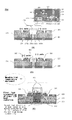
As shown in FIG. 3(A) , a multi-though hole of a two-tiered structure is formed at the double-sided substrate (FR-4 PCB) 200 by means of a punching process depending on the shape and size of the power LED.
The double-sided substrate (FR-4 PCB) is a means for positioning the power LED, and Cu thin surfaces 220 and 221 are attached to the upper and lower sides of the FR-4 material 210 which is formed of a solder pad helping fix the lead frame (+pole and −pole) of the power LED.
The double-sided substrate (FR-4 PCB) provides a PCB assembly (PCB Assy) which can help save a unit cost as compared with the expensive MC PCB (Metal core printed circuit board) and the thermal pad and can help make lighter the whole module members and can help obtain a good attachment flatness of the printed circuit board.
The multi-through hole 230 is a through hole member which accommodates a heat transfer medium for the sake of transferring a high temperature heat coming from the heat radiation point 190 of the power LED heat radiation portion 180 having a two-tiered structure, to the aluminum structure 600 which is a heat radiation structure. At the upper side of the double-sided substrate (FR-4 PCB) 200 is formed one through hole 231 at every portion where the power LED is positioned, and at the lower side extended from one through hole 231 is formed a plurality of through holes 232 a˜232 d by means of a punching process. At this time, it is noted that the lower Cu thin surface 221 of the double-sided substrate (FR-4 PCB) 200 is not punched.
Here, the lower Cu thin surface 221 of the double-sided substrate (FR-4 PCB) 200 is not punched the reasons that the high temperature heat coming from the power LED can be transferred to the aluminum structure 600, which is a large heat radiation structure, as it comes into contact with the Pb-free cream solder 300 soldered (Pb soldering) by means of a movable high temperature equipment 400.
As shown in FIG. 3 (B), it shows a state that the Pb-free cream solder 300 is filled in the through member with a multi-through hole of a two-tiered structure by means of a punching process depending on the shape and size of the power LED in the double-sided substrate (FR-4 PCB) 200.
The Pb-free cream solder 300 is a heat transfer medium with the function of a heat slug 310 and is injected in the multi-through hole 230 as high as the height of the solder pad by using a mechanical device.
As shown in FIG. 3(C) , it shows a state that a Pb-free cream solder 300 is filled injected into the through member with a multi-through hole of a two-tier structure by means of a punching process depending on the shape and size of the power LED 100 in the double-sized substrate (FR-4 PCB) 200, and it is soldered (Pb soldering) using a movable high temperature equipment 400.
The movable high temperature equipment 400 is a kind of equipment which fixes by supplying a high temperature heat to the Pb-free cream solder 300 by using a heat transfer medium and is featured in that the Pb-free cream solder 300 is soldered by positioning the power LED 100 at the electrode plates (+ and −) after the Pb-free cream solder 300 is soldered, and the solder pad 320 connecting with the lead frame (or anode and cathode) of the power LED 100 is soldered at a high temperature.
As shown in FIG. 4 , the PCB assembly (PCB Assy) 500 is a means which is formed by packaging the power LED 100, the double-sided substrate (FR-4 PCB) 200 and the Pb-free cream solder 300, in other words, it is a structured means formed by forming an anode electrode as a fixing type cradle structure with a Pb soldering structure so that, by means of the movable high temperature equipment 400, the heat radiation point 190 of the heating portion 180 of the backside of the power LED 100 and the Pb-free cream solder 300 injected into the multi-through hole 230 and the lower Cu thin surface 221 of the double-sided substrate (FR-4 PCB) are integrated as one body and become a heat transfer medium.
As shown in FIG. 5 , the PCB assembly 500 is constructed so as to maximize the heat radiation efficiency as a LED lighting as it is fixedly attached to the aluminum structure 600 which is a large heat radiation structure. In addition, it shows an actual size structure which can be used to manufacture a large LED lighting structure such as a streetlight by using it in multiple numbers.
In addition, FIG. 6 is a flow chart explaining a method for producing a large lighting with a power LED of FIGS. 3(A) , (B) and (C) through FIG. 5 .
As shown in FIG. 6 , the method for producing a large lighting with a power LED comprises:
(A) a step S100 in which one through hole is formed by means of a punching process at part of an upper side in order for a double-sided substrate not to be passed depending on the shape and size of the power LED in the double-sided substrate (FR-4 PCB) 200 in which a Cu thin surface 220, 221 is attached at the upper and lower portions made from a FR-4 material 210 having a solder pad 320 which can fix a lead frame (+pole and −pole) of the power LED.
(B) a step S200 in which a plurality of through holes 232 a˜232 d are formed by passing through the remaining parts of the double-sided substrate extended from one through hole 231, so a multi-through hole 230 of a two-tiered structure is formed in such a way that a lower Cu thin surface 221 of a double-sided substrate (FR-4 PCB) 200 is not punched.
As shown in FIG. 7 , the multi-through hole 230 of a two-tiered structure is characterized in that it is formed at a portion vertically matching with the heat radiant point 190 of the power LED heating portion 180 (S210).
In addition, the multi-through hole 230 of a two-tiered structure is characterized in that it is previously punched at the time of processing the double-sided substrate (FR-4 PCB) (S220).
In addition, the multi-through hole 230 of a two-tiered structure is punched in a circular shape 240 or a quadrangle shape 250 depending on the shape and size of the power LED (S230).
In addition, one through hole 231 is characterized in that the Pb-free cream solder 300 injected into one through hole 231 becomes a heat transfer medium of a Pb soldering structure by means of the movable high temperature equipment 400, thus accumulating the high temperature heat coming from the heat radiation point 190 of the power LED heat radiation portion 180 (S240).
The plurality of the through holes 232 a˜232 dare characterized in that they can fast disperse, in a multiplexing way, a high temperature heat accumulated at one through hole 231 (S250).
The key technical concept of the embodiment of the present invention lies in that there is provided a multi-through hole 230 of a two-tiered structure which is equipped with one through hole 231 and a plurality of the through holes 232 a˜232 d. In other words, the heat coming from the heat radiation point 190 of the power LED heat radiation portion 180 is characterized in that the current increases in order to enhance the light emitting efficiency in case of the large LED lighting such as a streetlight, and as the current rises, the temperature of the heat radiation point of the heating portion increases. The preset invention is directed to multiplying the heat radiation effects in such a way that the heat radiation coming from one through hole 231 accommodating a heat transfer medium having a function of a heat slug with a larger volume than the plurality of the through holes 232 a˜232 d is fast accumulated at the time it emits, and the high temperature radiation having a high thermal expansion coefficient is dispersed in a multiplexing way toward the plurality of the trough holes 232 a˜232 d having a smaller volume than one through hole 231 as in the Bernoulli's theorem in which the flowing speed becomes faster when a fluid passes from a wider tube to a narrow tube.
In other words, the heat coming from the heat radiation point 190 of the power LED heating portion 180 is firstly, quickly accumulated at a Pb-free cream solder 300 injected in one through hole 231 having a heat slug function. At this time, the heat radiation of the power LED accumulated at one through hole 231 has a high thermal expansion coefficient. The Pb-free cream solder 300 injected in the plurality of the through holes 232 a˜232 d can secondary, quickly radiate the heat accumulated at one through hole 231, thus disperse, in a multiplexing way, the heat accumulated in one through hole 231 now what the Pb-free cream solder 300 is directly Pb-soldered with the lower cu thin surface 221 of the double-sided substrate (FR-4 PCB) 200 by means of a soldering. In addition, the heat radiation effects can be thirdly maximized by spreading over a wider heat radiation range in such a way that it is fixedly attached with the lower Cu thin surface 221 of the double-sided substrate (FR-4 PCB) 200 and the aluminum structure 600 which is a large heat radiation structure.
The above-mentioned technical construction is a unique heat radiation design technology developed by the applicant of the present application which is not disclosed so far in the industry.
There is provided (C) a step S300 in which a Pb-free cream solder 300 is injected in the multi-through hole 230 of a two-tiered structure as much as the height of the solder pad for the purpose of providing a heat slug function by using a mechanical device.
As shown in FIG. 8 , the Pb-free cream solder 300 is characterized in that it is injected into the double-sided substrate (FR-4 PCB) 200 before the power LED is engaged (S310).
There is provided (D) a step S400 in which a PCB assembly (PCB Assy) 500 is finished by soldering a Pb-free cream solder 300 for the purpose of ensuring that the heat radiation point of the heating portion of a backside of the power LED and the Pb-free cream solder 300 and the lower Cu thin surface of the double-sided substrate are integrated, by using a movable high temperature equipment 400 after the power LED 100 is properly positioned at the pole plates following the injection of the Pb-free cream solder 300.
There is provided (E) a step S500 in which the PCB assembly 500 is engaged to an aluminum structure 600 which is a large heat radiation structure, thus maximizing the heat radiation efficiency of the LED lighting.
As shown in FIG. 8 , the PCB assembly 500 and the aluminum structure 600 which is a large heat radiation structure are characterized in that they are engaged by a soldering (Pb soldering) or a thermal grease (S510).
According to the preferred embodiment of the present invention, the present invention is characterized in that it is possible to propose a new applied technology on a heat radiation design method of a backside of a power LED device for the purpose of producing a large LED lighting appliance such as a streetlight in such a way that the high temperature can be fast dispersed, in a multiplexing way, into the temperature of the atmosphere, the high temperature heat being accumulated by means of a heat radiation point of a heating portion of a backside of a power LED and a thermal transfer medium in a multi-through hole helping come into direct contact with an aluminum structure which is a large heat radiation structure.
As the present invention may be embodied in several forms without departing from the spirit or essential characteristics thereof, it should also be understood that the above-described examples are not limited by any of the details of the foregoing description, unless otherwise specified, but rather should be construed broadly within its spirit and scope as defined in the appended claims, and therefore all changes and modifications that fall within the meets and bounds of the claims, or equivalences of such meets and bounds are therefore intended to be embraced by the appended claims.
Claims (8)
1. A method for producing a large lighting with a power LED, comprising:
(a) a step in which an opening is formed by means of a punching process at part of an upper side in order for a double-sided substrate not to be passed depending on the shape and size of the power LED in the double-sided substrate (FR-4 PCB) in which a Cu thin surface is attached at the upper and lower portions made from a FR-4 material having a solder pad which can fix a lead frame (+pole and −pole) of the power LED;
(b) a step in which a plurality of through holes are formed by passing through the remaining parts of the double-sided substrate extended from the opening, so a multi-through hole of a two-tiered structure is formed in such a way that a lower Cu thin surface of a double-sided substrate (FR-4 PCB) is not punched;
(c) a step in which a Pb-free cream solder is injected in the multi-through hole of a two-tiered structure as much as the height of the solder pad for the purpose of providing a heat slug function by using a mechanical device;
(d) a step in which a PCB assembly (PCB Assy) is finished by soldering a Pb-free cream solder for the purpose of ensuring that the heat radiation point of the heating portion of a backside of the power LED and the Pb-free cream solder and the lower Cu thin surface of the double-sided substrate are integrated, by using a movable high temperature equipment after the power LED is properly positioned at the pole plates following the injection of the Pb-free cream solder; and
(e) a step in which the PCB assembly is engaged to an aluminum structure which is a large heat radiation structure, thus maximizing the heat radiation efficiency of the LED lighting.
2. A method for producing a large lighting with a power LED according to claim 1 , wherein said multi-through hole of a two-tiered structure is punched at a portion where is vertically matched with a heat radiation point of the power LED heating portion.
3. A method for producing a large lighting with a power LED according to claim 2 , wherein said multi-through hole of a two-tiered structure is previously punched when processing the double-sided substrate (FR-4 PCB).
4. A method for producing a large lighting with a power LED according to claim 3 , wherein said multi-through hole of a two-tiered structure is punched in a circular shape or a quadrangle shape.
5. A method for producing a large lighting with a power LED according to claim 1 , wherein said opening has a function by which the Pb-free cream solder injected in the opening becomes a thermal transfer medium of a Pb soldering structure by means of a movable high temperature equipment, thus fast accumulating a high temperature heat coming from a heat radiation point of the power LED heating portion.
6. A method for producing a large lighting with a power LED according to claim 5 , wherein the plurality of said through holes have functions of dispersing, in a multiplexing way and a fast flow speed type, a high temperature heat fast accumulated in one through hole.
7. A method for producing a large lighting with a power LED according to claim 1 , wherein said PB-free cream solder is injected before the power LED is engaged to the double-sided substrate (FR-4 PCB).
8. A method for producing a large lighting with a power LED according to claim 1 , wherein said PCB assembly and said aluminum structure, which is a large heat radiation structure, are fixedly attached by a soldering or a thermal grease.
Applications Claiming Priority (3)
| Application Number | Priority Date | Filing Date | Title |
|---|---|---|---|
| KR1020090116242A KR100962706B1 (en) | 2009-11-27 | 2009-11-27 | Manufacture method of the large illuminations with power led |
| KR10-2009-0116242 | 2009-11-27 | ||
| PCT/KR2010/007755 WO2011065683A2 (en) | 2009-11-27 | 2010-11-04 | Method for producing large lighting with power l e d |
Related Parent Applications (1)
| Application Number | Title | Priority Date | Filing Date |
|---|---|---|---|
| PCT/KR2010/007755 A-371-Of-International WO2011065683A2 (en) | 2009-11-27 | 2010-11-04 | Method for producing large lighting with power l e d |
Related Child Applications (1)
| Application Number | Title | Priority Date | Filing Date |
|---|---|---|---|
| US13/968,317 Continuation US8878228B2 (en) | 2009-11-27 | 2013-08-15 | Method for producing large lighting with power LED |
Publications (2)
| Publication Number | Publication Date |
|---|---|
| US20130130418A1 US20130130418A1 (en) | 2013-05-23 |
| US8535959B2 true US8535959B2 (en) | 2013-09-17 |
Family
ID=42369876
Family Applications (2)
| Application Number | Title | Priority Date | Filing Date |
|---|---|---|---|
| US13/512,328 Expired - Fee Related US8535959B2 (en) | 2009-11-27 | 2010-11-04 | Method for producing large lighting with power LED |
| US13/968,317 Expired - Fee Related US8878228B2 (en) | 2009-11-27 | 2013-08-15 | Method for producing large lighting with power LED |
Family Applications After (1)
| Application Number | Title | Priority Date | Filing Date |
|---|---|---|---|
| US13/968,317 Expired - Fee Related US8878228B2 (en) | 2009-11-27 | 2013-08-15 | Method for producing large lighting with power LED |
Country Status (6)
| Country | Link |
|---|---|
| US (2) | US8535959B2 (en) |
| JP (1) | JP5735976B2 (en) |
| KR (1) | KR100962706B1 (en) |
| CN (1) | CN102695916B (en) |
| DE (1) | DE112010004593B4 (en) |
| WO (1) | WO2011065683A2 (en) |
Families Citing this family (8)
| Publication number | Priority date | Publication date | Assignee | Title |
|---|---|---|---|---|
| TWI489918B (en) * | 2012-11-23 | 2015-06-21 | 旭德科技股份有限公司 | Package carrier |
| KR20160108867A (en) * | 2015-03-09 | 2016-09-21 | 엘이디라이텍(주) | Flexible printed circuit board for LED lamp |
| CN105065951B (en) * | 2015-08-31 | 2018-07-20 | 宁波耐斯达光电有限公司 | A kind of collection floodlight is concentrated on integrated light source and its system |
| ES2597740B1 (en) * | 2016-10-05 | 2017-08-04 | Sacyr Concesiones, S.L. | ROAD TUNNEL LIGHTING SYSTEM |
| US10436416B2 (en) | 2017-07-19 | 2019-10-08 | Ford Global Technologies, Llc | Vehicle light assembly with heat sink |
| CN114551641B (en) * | 2022-02-10 | 2023-09-12 | 中国科学院上海技术物理研究所 | Thermal layer structure of focal plane detector for physically isolating coupling stress |
| CN116127903B (en) * | 2023-02-14 | 2023-11-14 | 电子科技大学 | A high-power PA chip layout and wind tunnel self-heating packaging design method |
| KR102622451B1 (en) * | 2023-08-10 | 2024-01-05 | 박은홍 | LED lighting apparatus |
Citations (8)
| Publication number | Priority date | Publication date | Assignee | Title |
|---|---|---|---|---|
| US20050035447A1 (en) * | 2003-01-15 | 2005-02-17 | Kyocera Corporation | Heat releasing member, package for accommodating semiconductor element and semiconductor device |
| KR100610650B1 (en) | 2005-06-17 | 2006-08-09 | (주) 파이오닉스 | LED package and manufacturing method |
| KR100851367B1 (en) | 2006-12-27 | 2008-08-08 | 서울반도체 주식회사 | Light emitting diode |
| KR100882588B1 (en) | 2007-08-16 | 2009-02-12 | 알티전자 주식회사 | Light emitting diode package |
| KR20090062070A (en) | 2007-12-12 | 2009-06-17 | 세종메탈 주식회사 | Metal circuit board with excellent heat dissipation and its manufacturing method |
| US20100123162A1 (en) * | 2008-11-18 | 2010-05-20 | Kondo Ryosuke | Optical semiconductor apparatus and method for producing the same |
| US20110001162A1 (en) * | 2008-04-18 | 2011-01-06 | Asahi Glass Company, Limited | Light emitting diode package |
| US20110127559A1 (en) * | 2009-11-30 | 2011-06-02 | Dong Hyun Yu | Light emission device package and method of fabricating the same |
Family Cites Families (11)
| Publication number | Priority date | Publication date | Assignee | Title |
|---|---|---|---|---|
| US6097089A (en) * | 1998-01-28 | 2000-08-01 | Mitsubishi Gas Chemical Company, Inc. | Semiconductor plastic package, metal plate for said package, and method of producing copper-clad board for said package |
| JPS5836500B2 (en) * | 1974-06-07 | 1983-08-09 | 株式会社日立製作所 | Manufacturing method of ceramic substrate for IC |
| US6498355B1 (en) * | 2001-10-09 | 2002-12-24 | Lumileds Lighting, U.S., Llc | High flux LED array |
| JP4305896B2 (en) * | 2002-11-15 | 2009-07-29 | シチズン電子株式会社 | High brightness light emitting device and manufacturing method thereof |
| DE102004016847A1 (en) * | 2004-04-07 | 2005-12-22 | P.M.C. Projekt Management Consult Gmbh | Light emitting diode arrangement and method for producing a light emitting diode array |
| US6964884B1 (en) * | 2004-11-19 | 2005-11-15 | Endicott Interconnect Technologies, Inc. | Circuitized substrates utilizing three smooth-sided conductive layers as part thereof, method of making same, and electrical assemblies and information handling systems utilizing same |
| DE202005018009U1 (en) * | 2005-06-30 | 2006-02-09 | Lite-On Technology Corporation | Semiconductor mounting structure for cooling e.g. LED chip sets includes conductive plates beneath base plate connected to a heat conductor by conductive wires |
| KR101263934B1 (en) * | 2006-05-23 | 2013-05-10 | 엘지디스플레이 주식회사 | Light emitting diode and method of manufacturing thesame |
| KR100854328B1 (en) * | 2006-07-07 | 2008-08-28 | 엘지전자 주식회사 | Light emitting device package and its manufacturing method |
| JP5142119B2 (en) * | 2006-09-20 | 2013-02-13 | 住友電装株式会社 | Method of manufacturing printed circuit board having heat dissipation structure and heat dissipation structure of printed circuit board manufactured by the method |
| JP2008078584A (en) * | 2006-09-25 | 2008-04-03 | Matsushita Electric Works Ltd | Light-emitting apparatus |
-
2009
- 2009-11-27 KR KR1020090116242A patent/KR100962706B1/en not_active Expired - Fee Related
-
2010
- 2010-11-04 WO PCT/KR2010/007755 patent/WO2011065683A2/en not_active Ceased
- 2010-11-04 JP JP2012541007A patent/JP5735976B2/en not_active Expired - Fee Related
- 2010-11-04 CN CN201080053924.8A patent/CN102695916B/en not_active Expired - Fee Related
- 2010-11-04 US US13/512,328 patent/US8535959B2/en not_active Expired - Fee Related
- 2010-11-04 DE DE112010004593.3T patent/DE112010004593B4/en not_active Expired - Fee Related
-
2013
- 2013-08-15 US US13/968,317 patent/US8878228B2/en not_active Expired - Fee Related
Patent Citations (8)
| Publication number | Priority date | Publication date | Assignee | Title |
|---|---|---|---|---|
| US20050035447A1 (en) * | 2003-01-15 | 2005-02-17 | Kyocera Corporation | Heat releasing member, package for accommodating semiconductor element and semiconductor device |
| KR100610650B1 (en) | 2005-06-17 | 2006-08-09 | (주) 파이오닉스 | LED package and manufacturing method |
| KR100851367B1 (en) | 2006-12-27 | 2008-08-08 | 서울반도체 주식회사 | Light emitting diode |
| KR100882588B1 (en) | 2007-08-16 | 2009-02-12 | 알티전자 주식회사 | Light emitting diode package |
| KR20090062070A (en) | 2007-12-12 | 2009-06-17 | 세종메탈 주식회사 | Metal circuit board with excellent heat dissipation and its manufacturing method |
| US20110001162A1 (en) * | 2008-04-18 | 2011-01-06 | Asahi Glass Company, Limited | Light emitting diode package |
| US20100123162A1 (en) * | 2008-11-18 | 2010-05-20 | Kondo Ryosuke | Optical semiconductor apparatus and method for producing the same |
| US20110127559A1 (en) * | 2009-11-30 | 2011-06-02 | Dong Hyun Yu | Light emission device package and method of fabricating the same |
Non-Patent Citations (1)
| Title |
|---|
| International Search Report for PCT/KR2010/007755 mailed Jun. 23, 2011. |
Also Published As
| Publication number | Publication date |
|---|---|
| CN102695916A (en) | 2012-09-26 |
| WO2011065683A2 (en) | 2011-06-03 |
| JP2013512560A (en) | 2013-04-11 |
| US20130130418A1 (en) | 2013-05-23 |
| DE112010004593T5 (en) | 2013-01-24 |
| KR100962706B1 (en) | 2010-06-15 |
| WO2011065683A3 (en) | 2011-09-01 |
| CN102695916B (en) | 2014-11-05 |
| US8878228B2 (en) | 2014-11-04 |
| JP5735976B2 (en) | 2015-06-17 |
| DE112010004593B4 (en) | 2016-12-15 |
| US20130328099A1 (en) | 2013-12-12 |
Similar Documents
| Publication | Publication Date | Title |
|---|---|---|
| US8878228B2 (en) | Method for producing large lighting with power LED | |
| US11543081B2 (en) | LED assembly with omnidirectional light field | |
| US8008845B2 (en) | Lighting device which includes one or more solid state light emitting device | |
| CN102472482B (en) | Solid state lighting device with improved heat sink | |
| US8035284B2 (en) | Distributed LED-based light source | |
| KR100975970B1 (en) | The large illuminations with power led | |
| JP2012503334A (en) | Optical disc for lighting module | |
| JP2012503332A (en) | Lighting module | |
| WO2012109059A2 (en) | Solid state lighting device with elongated heatsink | |
| WO2012027871A1 (en) | Led package with contrasting face | |
| US20110175511A1 (en) | Light emitting diode and light source module having same | |
| US20070246726A1 (en) | Package structure of light emitting device | |
| US7838986B2 (en) | Illumination device | |
| KR101028357B1 (en) | LED lighting fixture with heat dissipation | |
| Wall et al. | High-power LED package requirements | |
| US9443832B2 (en) | Light emitting device, light source for illumination, and illumination apparatus | |
| KR20060086057A (en) | Heat dissipation structure of LED package and LED package having the structure | |
| KR20090002281A (en) | LED module for lighting with improved heat dissipation | |
| KR100954858B1 (en) | A high-luminance led package and method for manufacturing thereof | |
| KR101133649B1 (en) | Electric/electronic apparatus and led apparatus which has high heat-release efficiency | |
| KR100670917B1 (en) | LED module for lighting | |
| KR200344157Y1 (en) | LED Lamp device of surface mounting device for prevent heat-deteriorating | |
| KR20090010001A (en) | Heat dissipation device of LED lighting module | |
| KR20080092001A (en) | Light Emitting Diode Module | |
| KR20110061698A (en) | Heat dissipation device of LED element with improved heat transfer efficiency |
Legal Events
| Date | Code | Title | Description |
|---|---|---|---|
| STCF | Information on status: patent grant |
Free format text: PATENTED CASE |
|
| FPAY | Fee payment |
Year of fee payment: 4 |
|
| FEPP | Fee payment procedure |
Free format text: MAINTENANCE FEE REMINDER MAILED (ORIGINAL EVENT CODE: REM.); ENTITY STATUS OF PATENT OWNER: MICROENTITY |
|
| LAPS | Lapse for failure to pay maintenance fees |
Free format text: PATENT EXPIRED FOR FAILURE TO PAY MAINTENANCE FEES (ORIGINAL EVENT CODE: EXP.); ENTITY STATUS OF PATENT OWNER: MICROENTITY |
|
| STCH | Information on status: patent discontinuation |
Free format text: PATENT EXPIRED DUE TO NONPAYMENT OF MAINTENANCE FEES UNDER 37 CFR 1.362 |
|
| FP | Lapsed due to failure to pay maintenance fee |
Effective date: 20210917 |