US8533573B2 - Error correction circuit and method thereof - Google Patents
Error correction circuit and method thereof Download PDFInfo
- Publication number
- US8533573B2 US8533573B2 US12/051,641 US5164108A US8533573B2 US 8533573 B2 US8533573 B2 US 8533573B2 US 5164108 A US5164108 A US 5164108A US 8533573 B2 US8533573 B2 US 8533573B2
- Authority
- US
- United States
- Prior art keywords
- decoding
- control signal
- signal
- correcting
- error
- Prior art date
- Legal status (The legal status is an assumption and is not a legal conclusion. Google has not performed a legal analysis and makes no representation as to the accuracy of the status listed.)
- Active, expires
Links
Images


Classifications
-
- H—ELECTRICITY
- H04—ELECTRIC COMMUNICATION TECHNIQUE
- H04L—TRANSMISSION OF DIGITAL INFORMATION, e.g. TELEGRAPHIC COMMUNICATION
- H04L25/00—Baseband systems
- H04L25/38—Synchronous or start-stop systems, e.g. for Baudot code
- H04L25/40—Transmitting circuits; Receiving circuits
- H04L25/49—Transmitting circuits; Receiving circuits using code conversion at the transmitter; using predistortion; using insertion of idle bits for obtaining a desired frequency spectrum; using three or more amplitude levels ; Baseband coding techniques specific to data transmission systems
- H04L25/4906—Transmitting circuits; Receiving circuits using code conversion at the transmitter; using predistortion; using insertion of idle bits for obtaining a desired frequency spectrum; using three or more amplitude levels ; Baseband coding techniques specific to data transmission systems using binary codes
- H04L25/4908—Transmitting circuits; Receiving circuits using code conversion at the transmitter; using predistortion; using insertion of idle bits for obtaining a desired frequency spectrum; using three or more amplitude levels ; Baseband coding techniques specific to data transmission systems using binary codes using mBnB codes
-
- H—ELECTRICITY
- H04—ELECTRIC COMMUNICATION TECHNIQUE
- H04L—TRANSMISSION OF DIGITAL INFORMATION, e.g. TELEGRAPHIC COMMUNICATION
- H04L25/00—Baseband systems
- H04L25/02—Details ; arrangements for supplying electrical power along data transmission lines
- H04L25/03—Shaping networks in transmitter or receiver, e.g. adaptive shaping networks
- H04L25/03006—Arrangements for removing intersymbol interference
- H04L25/03012—Arrangements for removing intersymbol interference operating in the time domain
- H04L25/03019—Arrangements for removing intersymbol interference operating in the time domain adaptive, i.e. capable of adjustment during data reception
-
- H—ELECTRICITY
- H04—ELECTRIC COMMUNICATION TECHNIQUE
- H04L—TRANSMISSION OF DIGITAL INFORMATION, e.g. TELEGRAPHIC COMMUNICATION
- H04L25/00—Baseband systems
- H04L25/02—Details ; arrangements for supplying electrical power along data transmission lines
- H04L25/03—Shaping networks in transmitter or receiver, e.g. adaptive shaping networks
- H04L25/03006—Arrangements for removing intersymbol interference
- H04L2025/0335—Arrangements for removing intersymbol interference characterised by the type of transmission
- H04L2025/03356—Baseband transmission
-
- H—ELECTRICITY
- H04—ELECTRIC COMMUNICATION TECHNIQUE
- H04L—TRANSMISSION OF DIGITAL INFORMATION, e.g. TELEGRAPHIC COMMUNICATION
- H04L25/00—Baseband systems
- H04L25/02—Details ; arrangements for supplying electrical power along data transmission lines
- H04L25/03—Shaping networks in transmitter or receiver, e.g. adaptive shaping networks
- H04L25/03006—Arrangements for removing intersymbol interference
- H04L2025/03592—Adaptation methods
- H04L2025/03598—Algorithms
Definitions
- the invention relates to an error correction circuit and method, and particularly to an error correction circuit and method for a DisplayPort receiver in order to improve the reliability of input data.
- DisplayPort is a new digital display interface standard put forth by the Video Electronics Standard Association (VESA), including a Main Link, an auxiliary channel (AUX CH), and a hot plug detect (HPD) signal line.
- VESA Video Electronics Standard Association
- Main Link is a high-bandwidth, low-latency, uni-directional interface used for transport of isochronous streams.
- the number of lanes of Main Link can be either 1, 2, or 4 lanes, providing digital video and audio for simultaneous streaming transmission.
- Each lane supports transmission at two link rates (F link ): 1.62 Gbps or 2.7 Gbps per lane. Therefore, DisplayPort offers up to 10.8 Gbps of bandwidth.
- a DisplayPort transmitter uses a PCI-EXPRESS-like link to send send image data and audio data together with a high speed link clock (having the link rates F link ) and encodes 8-bit data signals and 8-bit control signals into 10-bit dc-balanced signals by a ANSI 8B/10B encoder.
- a displayPort receiver uses a decoder to recover the 8-bit data signal and the 8-bit control signal.
- poor channel quality may result in erroneous received signals. Under such circumstances, corresponding original values are not found correctly at a decoding stage, making subsequent data to be determined incorrectly.
- FIG. 1 is an example showing a main video stream data packing over 4-lane Main Link.
- Main Link consists of four lanes L 0 ⁇ L 3 .
- a video data area follows a blanking end (BE) signal, whereas a blanking start (BS) signal is inserted immediately after the video data area.
- a VB-ID signal, a video time stamp value M vid 7:0, an audio time stamp value M aud 7:0 and audio data are inserted between the signals BS and BE. Errors generated in the video data area may cause incorrect pixel values displayed in a frame. If an error is included in one of the control signals such as the signals BS, BE and VB-ID, several important image control signals such as a vertical synchronization (VS) signal and a horizontal synchronization (HS) signal may not be constructed correctly in the receivers.
- VS vertical synchronization
- HS horizontal synchronization
- an object of the invention is to provide an error correction circuit which, if decoding errors occur at a decoding stage, actively adjusts settings of a physical layer by utilizing an ANSI 10B/8B decoder and performs data correction by means of digital logic circuitry, thus improving the reliability of input data.
- the error correction circuit which is applied to a digital display interface Sink device performs an error correction operation at a decoding stage, comprising: at least one converting circuit and a microprocessor.
- Each converting circuit comprises: an equalizer for amplifying an differential signal and generating an amplified signal; a clock data recovery circuit for receiving the amplified signal and generating a recovered data; a serial to parallel converter for performing serial to parallel conversion on the recovered data and generating a parallel data; and, a decoder for receiving the parallel data and generating a decoded data, a decoding control signal, a decoding error signal or selected combinations thereof.
- the microprocessor receives the decoding error signal and adjusts the equalizer, the clock data recovery circuit or both if a number of decoding errors of the decoding error signal is greater than a threshold value within a predetermined period of time.
- Another object of the invention is to provide an error correction correction method which is applied to a digital display interface Sink device and performs an error correction operation at a decoding stage.
- the method comprising the steps of: determining whether a number of decoding errors of a decoding error signal is greater than a threshold value within a predetermined period of time; and, adjusting a setting value to set a physical layer while the number of decoding errors is greater than the threshold value.
- Still another object of the invention is to provide an error correction method which is applied to a digital display interface Sink device and performs an error correction operation at a decoding stage.
- the method comprises the steps of: determining whether a number of decoding errors of a decoding error signal is greater than a threshold value within a predetermined period of time; and, correcting one or a plurality of corresponding signals according to the decoding error signal while the number of decoding errors is greater than the threshold value.
- FIG. 1 is an example showing a main video stream data packing over 4-lane Main Link.
- FIG. 2 is a block diagram showing an error correction circuit according to an embodiment of the invention.
- FIG. 3 is a flow chart illustrating how the strength of an equalizer is adjusted to reduce the number of decoding errors
- FIG. 4 is a timing diagram showing the timing relationship of a decoding control signal, a decoding error signal and a correcting control signal.
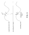
- FIG. 5 is a timing diagram showing original decoded data, a decoding error signal and correcting data.
- FIG. 6 is a flow chart illustrating a method of error correction of the invention.
- FIG. 2 is a block diagram showing an error correction circuit illustrated according to an embodiment of the invention.
- an error correction circuit 200 for a DisplayPort receiver includes an equalizer 211 , a clock data recovery (CDR) circuit 212 , a serial to parallel converter 213 , an ANSI 10B/8B decoder 214 , a correcting unit 250 and a microprocessor 260 .
- CDR clock data recovery
- a converting circuit 210 is installed in a lane L 0 of Main Link (a total of four converting circuits 210 would be needed if Main Link consists of four lanes).
- the equalizer 211 amplifies a differential signal to generate an amplified signal.
- the CDR circuit 212 includes a phased-locked loop (PLL) circuit (not shown) and sets a clock frequency of the PLL circuit according to a charge pump current value.
- the CDR circuit 212 receives and tracks the amplified signal to generate recovered data.
- the serial to parallel converter 213 performs a serial to parallel conversion on the recovered data to generate 10-bit parallel data.
- Original 8-bit data signals and 8-bit control signals are recovered from the 10-bit DC-balanced signals by the ANSI 10B/8B decoder 214 in the DisplayPort receiver.
- the ANSI 10B/8B decoder 214 receives and decodes the 10-bit parallel data to generate a decoding error signal DE 0 , decoding data D d0 and a decoding control signal CS 0 .
- both the decoding data D d0 and the decoding control signal CS 0 are 8-bit.
- the ANSI 10B/8B decoder 214 will generate a corresponding decoding error signal DE 0 (e.g., the decoding error signal DE 0 may be at a low voltage level during normal conditions and at a high voltage level when decoding results are deemed to be incorrect).
- the microprocessor 260 will try to fix the frequently-occurring decoding errors by readjusting the settings of the physical layer (For example, the strength of the equalizer 211 is adjusted by varying the gain value, and the tracking capability or the clock frequency of the CDR circuit 212 may be adjusted by varying the charge pump current value).
- FIGS. 2 and 3 describe how the strength of the equalizer is adjusted to fix the frequently-occurring decoding errors, and the converting circuit 210 in lane L 0 is being taken as an example.
- Step S 310 Operating normally, the error correcting circuit 200 sets the equalizer 211 by using a gain value (may be equal to a gain minimum value).
- Step S 320 A predetermined period T has elapsed, such as 1 ms.
- Step S 330 According to a decoding error signal DE 0 , the microprocessor 260 determines whether the number N DE0 of decoding errors is greater than a threshold value. If YES, the flow advances to the step S 340 ; otherwise, it indicates that the number N DE0 lies within the range of tolerance. Thus, the current gain value g is retained and the flow returns to the step S 310 .
- Step S 340 Determine whether the current gain value g is equal to a gain maximum value. If YES, the flow returns to the step S 310 ; otherwise, the flow advances to the step S 350 .
- the microprocessor 260 increases the gain value g from the minimum value to the maximum value and then observes corresponding variations in the measured number N DE0 of decoding errors. As long as the number N DE0 of decoding errors falls below the threshold value, it proves successful in adjusting the equalizer and then the loop is exited. On the contrary, if the gain value g is increased from the minimum to the maximum and the number N DE0 of decoding errors remains in a sense that nothing is improving, adjusting the equalizer would represent a failure. At this moment, by turning to the adjustment of the CDR circuit 212 is well worth a try. A method of adjusting the charge pump current value for reducing frequently-occurring decoding errors is similar to the method of FIG. 3 and thus will not be described herein.
- the worst case is that the number N DE of decoding errors does not reduce and is still greater than the threshold value even though both the gain value and the charge pump value have been adjusted from the minimum to the maximum. This indicates the adjustment is beyond the hardware capability of the physical layer and apparently the signal itself is incorrect. Accordingly, users may debug the transmitter or check the channel status to identify where the problem is.
- the above-mentioned physical layer adjusting mechanism is unable to recover the data or the control signals that have decoding errors that are already generated.
- a correcting unit 250 is necessary for recovering the data or the control signals that have the decoding errors, thus reducing the adverse effects as far as possible.
- the correcting unit 250 may receive one to four sets of output signals (including a decoding error signal, decoding data and a decoding control signal) of the converting circuits 210 to generate at least one correcting signal.
- the correcting signal includes a correcting control signal, a correcting data or combinations thereof. The operations of the correcting unit 250 will be described as follows.
- Main Link includes one lane only
- most of its control signals such as the blanking start signal BS, the blanking end signal BE and the signal VB_ID (since DisplayPort defines numerous control signals, only the blanking start signal BS of FIG. 4 is currently taken as an example)
- the blanking start signal BS is supposed to be present but appears to be absent along with a decoding error (i.e., the decoding error signal at a high voltage level) generated by the ANSI 10B/8B decoder 214
- the correcting unit 250 will actively recover the blanking start signal BS.
- the correcting unit 250 will insert a blanking start signal BS′ (e.g., signal at a high voltage level) in the corresponding location of the correcting control signal as shown in FIG. 4 , in which the blanking start signal BS is previously absent.
- a blanking start signal BS′ e.g., signal at a high voltage level
- a converting circuit 210 is installed in each lane and output signals of all converting circuits are transmitted to the same correcting unit 250 .
- An error correcting circuit (not shown) of the invention may include four converting circuits 210 , a microprocessor 260 and a correcting unit 250 .
- the correcting unit 250 receives four sets of output signals of four converting circuits, including decoding error signals DE 0 ⁇ DE 3 , decoding data D d0 ⁇ Dd 3 and decoding control signals CS 0 ⁇ CS 3 .
- control signals such as the blanking start signal BS and the blanking end signal BE
- BS and BE blanking start signal
- BE blanking end signal
- Main Link includes four lanes
- the correcting units 250 performs inter-lane de-skewing and simultaneously compares four sets of the decoding data D d0 ⁇ D d3 and four sets of the decoding control signals CS 0 ⁇ CS 3 .
- the correcting unit 250 will recover a corresponding blanking start signal BS in the set of the decoding control signal CS 3 according to the blanking start signals BS in the other three sets of decoding control signals CS 0 ⁇ CS 2 .
- the correcting units 250 will abandon a pixel value b of the original decoded data and derive a new pixel value b′ from its neighboring pixel values a, c.
- the new pixel value b′ is obtained by either passing pixel values a, c through a low-pass filter or performing an interpolation operation on the pixel values a, c.
- the correcting units 250 adopts the same method if the decoding error occurs in the audio data area.
- FIG. 6 is a flow chart illustrating a method of error correction of the invention. A method of error correction for DisplayPort receivers will be described in detail in accordance with FIGS. 2 and 6 .
- Step S 610 The error correcting circuit 200 operates normally and a predetermined period T has elapsed.
- Step S 620 According to the decoding error signal DE 0 (or DE 1 , or DE 2 , or DE 3 ), the microprocessor 260 determines whether the numberN DE0 (or N DE1 , or N DE2 , or N DE3 ) of decoding errors is greater than a threshold value. If YES, the flow advances to the step S 630 ; otherwise, it indicates that the number N DE0 (or N DE1 , or N DE2 , or N DE3 ) of decoding errors lies in the range of tolerance and then the flow returns to the step S 610 .
- Step S 630 If the number N DE0 (or N DE1 , or N DE2 , or N DE3 ) is greater than the threshold value, the correcting unit 250 receives the decoding error signal DE 0 (or DE 0 ⁇ DE 3 ), the decoded data D d0 (or D d0 ⁇ Dd 3 ) and the decoding control signal CS 0 (or CS 0 ⁇ CS 3 ) so as to recover control signals, audio signals and video signals correspondingly. Then, the flow advances to the step S 640 .
- Step S 640 If the number N DE0 (or N DE1 , or N DE2 , or N DE3 ) is greater than the threshold value, the microprocessor 260 adjusts the settings of the physical layer and the flow returns to the step S 610 .
- N DE0 or N DE1 , or N DE2 , or N DE2 or N DE3
- the first approach is to recover the data or the control signals having generated errors (step S 630 ) as far as possible.
- the second approach is to improve the quality of the subsequent input signals (step S 640 ), which can be achieved by adjusting the settings of the physical layer in the receivers.
- a poor input signal quality is caused by a transmitter or a poor channel condition, it is hard to improve by adjusting the settings of the physical layer on the receiver side.
- the method of FIG. 6 that simultaneously adopts the two different approaches achieves a significant effect on reducing the frequently-occurring decoding errors.
Landscapes
- Engineering & Computer Science (AREA)
- Computer Networks & Wireless Communication (AREA)
- Signal Processing (AREA)
- Power Engineering (AREA)
- Physics & Mathematics (AREA)
- Spectroscopy & Molecular Physics (AREA)
- Detection And Prevention Of Errors In Transmission (AREA)
Abstract
An error correction circuit and method applicable to a DisplayPort receiver is disclosed. While decoding errors occur at a decoding stage, the invention actively adjusts settings of a physical layer by using an ANSI10B/8B decoder and performs data recovery by using a correcting unit that improves the reliability of input data.
Description
This application claims priority of Application No. 096109829 filed in Taiwan, R.O.C. on Mar. 22, 2007 under 35 USC §119, the entire contents of which are hereby incorporated by reference.
1. Field of the Invention
The invention relates to an error correction circuit and method, and particularly to an error correction circuit and method for a DisplayPort receiver in order to improve the reliability of input data.
2. Description of the Related Art
DisplayPort is a new digital display interface standard put forth by the Video Electronics Standard Association (VESA), including a Main Link, an auxiliary channel (AUX CH), and a hot plug detect (HPD) signal line. Main Link is a high-bandwidth, low-latency, uni-directional interface used for transport of isochronous streams. The number of lanes of Main Link can be either 1, 2, or 4 lanes, providing digital video and audio for simultaneous streaming transmission. Each lane supports transmission at two link rates (Flink): 1.62 Gbps or 2.7 Gbps per lane. Therefore, DisplayPort offers up to 10.8 Gbps of bandwidth.
A DisplayPort transmitter uses a PCI-EXPRESS-like link to send send image data and audio data together with a high speed link clock (having the link rates Flink) and encodes 8-bit data signals and 8-bit control signals into 10-bit dc-balanced signals by a ANSI 8B/10B encoder. Reversely, a displayPort receiver uses a decoder to recover the 8-bit data signal and the 8-bit control signal. However, poor channel quality may result in erroneous received signals. Under such circumstances, corresponding original values are not found correctly at a decoding stage, making subsequent data to be determined incorrectly.
In view of the above-mentioned problems, an object of the invention is to provide an error correction circuit which, if decoding errors occur at a decoding stage, actively adjusts settings of a physical layer by utilizing an ANSI 10B/8B decoder and performs data correction by means of digital logic circuitry, thus improving the reliability of input data.
To achieve the above-mentioned object, the error correction circuit which is applied to a digital display interface Sink device performs an error correction operation at a decoding stage, comprising: at least one converting circuit and a microprocessor. Each converting circuit comprises: an equalizer for amplifying an differential signal and generating an amplified signal; a clock data recovery circuit for receiving the amplified signal and generating a recovered data; a serial to parallel converter for performing serial to parallel conversion on the recovered data and generating a parallel data; and, a decoder for receiving the parallel data and generating a decoded data, a decoding control signal, a decoding error signal or selected combinations thereof. The microprocessor receives the decoding error signal and adjusts the equalizer, the clock data recovery circuit or both if a number of decoding errors of the decoding error signal is greater than a threshold value within a predetermined period of time.
Another object of the invention is to provide an error correction correction method which is applied to a digital display interface Sink device and performs an error correction operation at a decoding stage. The method comprising the steps of: determining whether a number of decoding errors of a decoding error signal is greater than a threshold value within a predetermined period of time; and, adjusting a setting value to set a physical layer while the number of decoding errors is greater than the threshold value.
Still another object of the invention is to provide an error correction method which is applied to a digital display interface Sink device and performs an error correction operation at a decoding stage. The method comprises the steps of: determining whether a number of decoding errors of a decoding error signal is greater than a threshold value within a predetermined period of time; and, correcting one or a plurality of corresponding signals according to the decoding error signal while the number of decoding errors is greater than the threshold value.
Further scope of the applicability of the present invention will become apparent from the detailed description given hereinafter. However, it should be understood that the detailed description and specific examples, while indicating preferred embodiments of the invention, are given by way of illustration only, since various changes and modifications within the spirit and scope of the invention will become apparent to those skilled in the art from this detailed description.
The present invention will become more fully understood from the detailed description given herein below and the accompanying drawings which are given by way of illustration only, and thus are not limitative of the present invention, and wherein:
The invention will be described with reference to the accompanying drawings.
Referring to FIG. 2 , an error correction circuit 200 for a DisplayPort receiver includes an equalizer 211, a clock data recovery (CDR) circuit 212, a serial to parallel converter 213, an ANSI 10B/8B decoder 214, a correcting unit 250 and a microprocessor 260.
A converting circuit 210 is installed in a lane L0 of Main Link (a total of four converting circuits 210 would be needed if Main Link consists of four lanes). According to a gain value g, the equalizer 211 amplifies a differential signal to generate an amplified signal. The CDR circuit 212 includes a phased-locked loop (PLL) circuit (not shown) and sets a clock frequency of the PLL circuit according to a charge pump current value. The CDR circuit 212 receives and tracks the amplified signal to generate recovered data. The serial to parallel converter 213 performs a serial to parallel conversion on the recovered data to generate 10-bit parallel data. Original 8-bit data signals and 8-bit control signals are recovered from the 10-bit DC-balanced signals by the ANSI 10B/8B decoder 214 in the DisplayPort receiver. The ANSI 10B/8B decoder 214 receives and decodes the 10-bit parallel data to generate a decoding error signal DE0, decoding data Dd0 and a decoding control signal CS0.
Here, both the decoding data Dd0 and the decoding control signal CS0 are 8-bit. As long as certain number of bytes in either the decoding data Dd0 or the decoding control signal CS0 are corrupted and thus unable to be decoded correctly during transmission, the ANSI 10B/8B decoder 214 will generate a corresponding decoding error signal DE0 (e.g., the decoding error signal DE0 may be at a low voltage level during normal conditions and at a high voltage level when decoding results are deemed to be incorrect).
If decoding errors occur frequently (a number NDE0 of decoding errors is greater than a threshold value during a predetermined period), the microprocessor 260 will try to fix the frequently-occurring decoding errors by readjusting the settings of the physical layer (For example, the strength of the equalizer 211 is adjusted by varying the gain value, and the tracking capability or the clock frequency of the CDR circuit 212 may be adjusted by varying the charge pump current value). Hereinafter, FIGS. 2 and 3 describe how the strength of the equalizer is adjusted to fix the frequently-occurring decoding errors, and the converting circuit 210 in lane L0 is being taken as an example.
Step S310: Operating normally, the error correcting circuit 200 sets the equalizer 211 by using a gain value (may be equal to a gain minimum value).
Step S320: A predetermined period T has elapsed, such as 1 ms.
Step S330: According to a decoding error signal DE0, the microprocessor 260 determines whether the number NDE0 of decoding errors is greater than a threshold value. If YES, the flow advances to the step S340; otherwise, it indicates that the number NDE0 lies within the range of tolerance. Thus, the current gain value g is retained and the flow returns to the step S310.
Step S340: Determine whether the current gain value g is equal to a gain maximum value. If YES, the flow returns to the step S310; otherwise, the flow advances to the step S350.
Step S350: The current gain value g is increased by a unit (for example, g=g+1) and then used to set the equalizer 211. Afterward, the flow returns to the step S310.
In general, the microprocessor 260 increases the gain value g from the minimum value to the maximum value and then observes corresponding variations in the measured number NDE0 of decoding errors. As long as the number NDE0 of decoding errors falls below the threshold value, it proves successful in adjusting the equalizer and then the loop is exited. On the contrary, if the gain value g is increased from the minimum to the maximum and the number NDE0 of decoding errors remains in a sense that nothing is improving, adjusting the equalizer would represent a failure. At this moment, by turning to the adjustment of the CDR circuit 212 is well worth a try. A method of adjusting the charge pump current value for reducing frequently-occurring decoding errors is similar to the method of FIG. 3 and thus will not be described herein.
During the process of adjusting the settings of the physical layer, layer, the worst case is that the number NDE of decoding errors does not reduce and is still greater than the threshold value even though both the gain value and the charge pump value have been adjusted from the minimum to the maximum. This indicates the adjustment is beyond the hardware capability of the physical layer and apparently the signal itself is incorrect. Accordingly, users may debug the transmitter or check the channel status to identify where the problem is.
However, the above-mentioned physical layer adjusting mechanism is unable to recover the data or the control signals that have decoding errors that are already generated. A correcting unit 250 is necessary for recovering the data or the control signals that have the decoding errors, thus reducing the adverse effects as far as possible. Depending on the number of lanes of Main Link, the correcting unit 250 may receive one to four sets of output signals (including a decoding error signal, decoding data and a decoding control signal) of the converting circuits 210 to generate at least one correcting signal. Here, the correcting signal includes a correcting control signal, a correcting data or combinations thereof. The operations of the correcting unit 250 will be described as follows.
On condition that Main Link includes one lane only, referring to to FIGS. 2 and 4 , most of its control signals, such as the blanking start signal BS, the blanking end signal BE and the signal VB_ID (since DisplayPort defines numerous control signals, only the blanking start signal BS of FIG. 4 is currently taken as an example), are periodically generated. Whenever the blanking start signal BS is supposed to be present but appears to be absent along with a decoding error (i.e., the decoding error signal at a high voltage level) generated by the ANSI 10B/8B decoder 214, the correcting unit 250 will actively recover the blanking start signal BS. That is, the correcting unit 250 will insert a blanking start signal BS′ (e.g., signal at a high voltage level) in the corresponding location of the correcting control signal as shown in FIG. 4 , in which the blanking start signal BS is previously absent.
In a scenario that Main Link includes more than two lanes, a converting circuit 210 is installed in each lane and output signals of all converting circuits are transmitted to the same correcting unit 250. Take a Main Link including four lanes as an example. An error correcting circuit (not shown) of the invention may include four converting circuits 210, a microprocessor 260 and a correcting unit 250. Here, the correcting unit 250 receives four sets of output signals of four converting circuits, including decoding error signals DE0˜DE3, decoding data Dd0˜Dd3 and decoding control signals CS0˜CS3.
Since conventional DisplayPort transmitters perform an inter-lane inter-lane skewing (as shown in FIG. 1 ), control signals (such as the blanking start signal BS and the blanking end signal BE) on each lane are skewed to each other so as to prevent the same control signals on each lane from being damaged simultaneously if an unpredictable situation occurs at a certain moment. On condition that Main Link includes four lanes, after receiving four sets of the decoding error signals DE0˜DE3, the decoding data Dd0˜Dd3 and the decoding control signals CS0˜CS3, the correcting units 250 performs inter-lane de-skewing and simultaneously compares four sets of the decoding data Dd0˜Dd3 and four sets of the decoding control signals CS0˜CS3. During the comparing process, assuming that at a time point t0, three sets of decoding control signals CS0˜CS2 contain a blanking start signal BS but the set of decoding control signal CS3 doesn't, and that a decoding error occurs simultaneously while the ANSI 10B/8B decoder 214 produces the set of the decoding control signal CS3, the correcting unit 250 will recover a corresponding blanking start signal BS in the set of the decoding control signal CS3 according to the blanking start signals BS in the other three sets of decoding control signals CS0˜CS2.
On the other hand, if a decoding error occurs in the video data area, referring to FIG. 5 , the correcting units 250 will abandon a pixel value b of the original decoded data and derive a new pixel value b′ from its neighboring pixel values a, c. For example, the new pixel value b′ is obtained by either passing pixel values a, c through a low-pass filter or performing an interpolation operation on the pixel values a, c. Likewise, the correcting units 250 adopts the same method if the decoding error occurs in the audio data area.
Step S610: The error correcting circuit 200 operates normally and a predetermined period T has elapsed.
Step S620: According to the decoding error signal DE0 (or DE1, or DE2, or DE3), the microprocessor 260 determines whether the numberNDE0(or NDE1, or NDE2, or NDE3) of decoding errors is greater than a threshold value. If YES, the flow advances to the step S630; otherwise, it indicates that the number NDE0 (or NDE1, or NDE2, or NDE3) of decoding errors lies in the range of tolerance and then the flow returns to the step S610.
Step S630: If the number NDE0 (or NDE1, or NDE2, or NDE3) is greater than the threshold value, the correcting unit 250 receives the decoding error signal DE0 (or DE0˜DE3), the decoded data Dd0 (or Dd0˜Dd3) and the decoding control signal CS0 (or CS0˜CS3) so as to recover control signals, audio signals and video signals correspondingly. Then, the flow advances to the step S640.
Step S640: If the number NDE0 (or NDE1, or NDE2, or NDE3) is greater than the threshold value, the microprocessor 260 adjusts the settings of the physical layer and the flow returns to the step S610.
It should be noted that, if the number NDE0 (or NDE1, or NDE2, or NDE2 or NDE3) is greater than a threshold value, two approaches have been adopted simultaneously in the flow chart of FIG. 6 . The first approach is to recover the data or the control signals having generated errors (step S630) as far as possible. The second approach is to improve the quality of the subsequent input signals (step S640), which can be achieved by adjusting the settings of the physical layer in the receivers. However, if a poor input signal quality is caused by a transmitter or a poor channel condition, it is hard to improve by adjusting the settings of the physical layer on the receiver side. Obviously, the method of FIG. 6 that simultaneously adopts the two different approaches achieves a significant effect on reducing the frequently-occurring decoding errors. In an alternative embodiment, even if only one of the two approaches is employed, it still provides practical help in reducing the decoding errors.
While certain exemplary embodiments have been described and shown in the accompanying drawings, it is to be understood that such embodiments are merely illustrative of and not restrictive on the broad invention, and that this invention should not be limited to the specific construction and arrangement shown and described, since various other modifications may occur to those ordinarily skilled in the art.
Claims (24)
1. A method for error correction, the method comprising the steps of:
determining whether a number of decoding errors of a decoding error signal is greater than a threshold value within a predetermined period of time;
adjusting a setting value of a digital display interface while the number of decoding errors is greater than the threshold value during a decoding stage; and
correcting a decoding error of a decoding control signal of a lane according to corresponding decoding control signals residing in other lanes.
2. The method according to claim 1 , wherein the digital display interface is a DisplayPort interface.
3. The method according to claim 1 , wherein the step of adjusting the setting value comprises:
adjusting a gain value to set an equalizer.
4. The method according to claim 1 , wherein the step of adjusting the setting value comprises:
adjusting a charge pump current value to set a clock data recovery circuit.
5. The method according to claim 1 , wherein the step of adjusting the setting value comprises:
comparing the setting value with a predetermined maximum value; and
raising the setting value while the setting value is less than the predetermined maximum value.
6. The method according to claim 5 , wherein the step of adjusting the setting value further comprises:
setting the setting value to be equal to the predetermined maximum value while the setting value is greater than the predetermined maximum value.
7. A method for error correction, the method comprising the steps of:
determining whether a number of decoding errors of a decoding error signal is greater than a threshold value within a predetermined period of time: and
correcting a decoding error of a decoding control signal of a lane according to corresponding decoding control signals residing in other lanes,
wherein the method is applied to a digital display interface comprising a Main link with at least two lanes at a decoding stage.
8. A method for error correction, the method comprising the steps of:
determining whether a number of decoding errors of a decoding error signal is greater than a threshold value within a predetermined period of time; and
correcting a decoding error of a decoding control signal of a lane according to a pattern of the decoding control signal itself,
wherein the method is applied to a digital display interface comprising a Main link with only one lane at a decoding stage.
9. The method according to claim 8 , wherein the decoding control signal is a periodic signal.
10. The method according to claim 9 , wherein the decoding control signal comprises a blanking start signal, a blanking end signal, a signal VB_ID signal or selected combinations thereof.
11. A method for error correction, the method comprising the steps of:
determining whether a number of decoding errors of a decoding error signal is greater than a threshold value within a predetermined period of time; and
correcting erroneous decoded video data signal or erroneous decoding audio data signal by interpolation or low-pass filtering,
wherein the method is applied to a digital display interface at a decoding stage, and
wherein the digital display interface is a DisplayPort interface.
12. An error correction circuit, comprising: at least one converting circuit, each comprising:
an equalizer for amplifying a differential signal and generating an amplified signal;
a clock data recovery circuit for receiving the amplified signal and generating a recovered data;
a serial to parallel converter for generating a parallel data according to the recovered data;
a decoder of a digital display interface for generating a decoded data, a decoding control signal, a decoding error signal or selected combinations thereof according to the parallel data;
a microprocessor configured to adjust the equalizer, the clock data recovery circuit or both according to the decoding error signal if a number of decoding errors of the decoding error signal is greater than a threshold value within a predetermined period of time; and
a correcting unit configured to generate a correcting control signal correcting a decoding error of the decoding control signal of a lane to corresponding decoding control signals residing in other lanes.
13. The circuit according to claim 12 , wherein the digital display interface is a DisplayPort interface.
14. The circuit according to claim 12 , wherein one converting circuit is installed in one lane of the digital display interface.
15. The method according to claim 7 , wherein the digital display interface is a DisplayPort interface.
16. The method according to claim 8 , wherein the digital display interface is a DisplayPort interface.
17. The method according to claim 1 , wherein the correcting step includes correcting the decoding error of the decoding control signal of the lane according to the pattern of the decoding control signal itself, and the method is applied to a digital display interface comprising a Main link with only one lane at a decoding stage.
18. The method according to claim 1 , wherein the correcting step includes correcting the decoding error of the decoding control signal of the lane according to the corresponding decoding control signals residing in the other lanes, and the method is applied to a digital display interface comprising a Main link with at least two lanes at a decoding stage.
19. The error correction circuit according to claim 12 , wherein the correcting unit is configured to generate the correcting control signal correcting the decoding error of the decoding control signal of the lane according to the pattern of the decoding control signal itself, and the digital display interface comprises a Main link with only one lane at a decoding stage.
20. The error correction circuit according to claim 12 , wherein the correcting unit is configured to generate the correcting control signal correcting the decoding error of the decoding control signal of the lane according to the corresponding decoding control signals residing in other the lanes, and the digital display interface comprises a Main link with at least two lanes at a decoding stage.
21. A method for error correction, the method comprising the steps of:
determining whether a number of decoding errors of a decoding error signal is greater than a threshold value within a predetermined period of time;
adjusting a setting value of a digital display interface while the number of decoding errors is greater than the threshold value during a decoding stage; and
correcting a decoding error of a decoding control signal of a lane according to a pattern of the decoding control signal itself, wherein the pattern of the decoding control signal is a periodic pattern.
22. An error correction circuit, comprising:
at least one converting circuit, each comprising:
an equalizer for amplifying a differential signal and generating an amplified signal;
a clock data recovery circuit for receiving the amplified signal and generating a recovered data;
a serial to parallel converter for generating a parallel data according to the recovered data and; and
a decoder of a digital display interface for generating a decoded data, a decoding control signal, a decoding error signal or selected combinations thereof according to the parallel data; and
a microprocessor configured to adjust the equalizer, the clock data recovery circuit or both according to the decoding error signal if a number of decoding errors of the decoding error signal is greater than a threshold value within a predetermined period of time,
a correcting unit configured to generate a correcting control signal correcting a decoding error of the decoding control signal of a lane according to a pattern of the decoding control signal itself, wherein the pattern of the decoding control signal is a periodic pattern.
23. The method according to claim 21 , wherein the step of correcting the decoding error of the decoding control signal of the lane according to the pattern of the decoding control signal itself includes correcting the decoding error of the decoding control signal of the lane according to a missing part of the periodic pattern of the decoding control signal itself.
24. The circuit according to claim 22 , wherein the correcting unit is configured to generate the correcting control signal correcting the decoding error of the decoding control signal of the lane according to a missing part of the periodic pattern of the decoding control signal itself.
Applications Claiming Priority (3)
| Application Number | Priority Date | Filing Date | Title |
|---|---|---|---|
| TW096109829 | 2007-03-22 | ||
| TW096109829A TWI365615B (en) | 2007-03-22 | 2007-03-22 | Receiver of a displayport interface having an error correction circuit and method applied to the receiver |
| TW96109829A | 2007-03-22 |
Publications (2)
| Publication Number | Publication Date |
|---|---|
| US20080235551A1 US20080235551A1 (en) | 2008-09-25 |
| US8533573B2 true US8533573B2 (en) | 2013-09-10 |
Family
ID=39775934
Family Applications (1)
| Application Number | Title | Priority Date | Filing Date |
|---|---|---|---|
| US12/051,641 Active 2031-05-09 US8533573B2 (en) | 2007-03-22 | 2008-03-19 | Error correction circuit and method thereof |
Country Status (2)
| Country | Link |
|---|---|
| US (1) | US8533573B2 (en) |
| TW (1) | TWI365615B (en) |
Families Citing this family (12)
| Publication number | Priority date | Publication date | Assignee | Title |
|---|---|---|---|---|
| TWI452903B (en) * | 2009-07-10 | 2014-09-11 | Himax Media Solutions Inc | Vertical blanking interval decoder and operating method thereof |
| US8750176B2 (en) * | 2010-12-22 | 2014-06-10 | Apple Inc. | Methods and apparatus for the intelligent association of control symbols |
| US9838226B2 (en) | 2012-01-27 | 2017-12-05 | Apple Inc. | Methods and apparatus for the intelligent scrambling of control symbols |
| US8897398B2 (en) | 2012-01-27 | 2014-11-25 | Apple Inc. | Methods and apparatus for error rate estimation |
| US8990645B2 (en) | 2012-01-27 | 2015-03-24 | Apple Inc. | Methods and apparatus for error rate estimation |
| US9450790B2 (en) | 2013-01-31 | 2016-09-20 | Apple Inc. | Methods and apparatus for enabling and disabling scrambling of control symbols |
| US8917194B2 (en) | 2013-03-15 | 2014-12-23 | Apple, Inc. | Methods and apparatus for context based line coding |
| US9210010B2 (en) | 2013-03-15 | 2015-12-08 | Apple, Inc. | Methods and apparatus for scrambling symbols over multi-lane serial interfaces |
| TWI543596B (en) * | 2013-12-26 | 2016-07-21 | 晨星半導體股份有限公司 | Multimedia interface receiving circuit |
| KR102151949B1 (en) * | 2013-12-30 | 2020-09-04 | 엘지디스플레이 주식회사 | Display device and driving method thereof |
| US10699618B2 (en) * | 2018-05-03 | 2020-06-30 | Novatek Microelectronics Corp. | Integrated circuit and anti-interference method thereof |
| TWI739558B (en) | 2020-08-20 | 2021-09-11 | 群聯電子股份有限公司 | Signal receiving circuit, memory storage device and calibration method of equalizer circuit |
Citations (21)
| Publication number | Priority date | Publication date | Assignee | Title |
|---|---|---|---|---|
| US6182264B1 (en) * | 1998-05-22 | 2001-01-30 | Vlsi Technology, Inc. | Smart dynamic selection of error correction methods for DECT based data services |
| CN1304609A (en) | 1998-06-02 | 2001-07-18 | 摩托罗拉公司 | Method in selective call radio for decoding interleaved data block received as radio signal |
| US6332207B1 (en) * | 1997-12-08 | 2001-12-18 | Maxtor Corporation | Method of correcting a read error in a disk drive |
| US20030056168A1 (en) * | 2001-09-14 | 2003-03-20 | Koninklijke Philips Electronics N.V. | Encoder redundancy selection system and method |
| US6735735B1 (en) * | 1999-07-12 | 2004-05-11 | Hitachi, Ltd. | Forward error correcting code encoding equipment, forward error correcting code decoding equipment, and transmission apparatus |
| US20040240599A1 (en) | 2003-05-27 | 2004-12-02 | Mitsubishi Denki Kabushiki Kaisha | Half-rate clock and data recovery circuit |
| US20050091051A1 (en) * | 2002-03-08 | 2005-04-28 | Nippon Telegraph And Telephone Corporation | Digital signal encoding method, decoding method, encoding device, decoding device, digital signal encoding program, and decoding program |
| US20050149814A1 (en) * | 1999-10-20 | 2005-07-07 | Agazzi Oscar E. | Diagnostics of cable and link performance for a high-speed communication system |
| US20060072926A1 (en) * | 2003-06-03 | 2006-04-06 | Fujitsu Limited | Optical signal receiver, and method for controlling identification point for binarization processing performed thereby |
| US20060233230A1 (en) | 2005-04-06 | 2006-10-19 | Matsushita Electric Industrial Co., Ltd. | Equalization apparatus and equalization method |
| EP1753157A1 (en) * | 2005-04-28 | 2007-02-14 | Matsushita Electric Industrial Co., Ltd. | Digital broadcasting receiver |
| US20070156725A1 (en) * | 2005-12-16 | 2007-07-05 | Andreas Ehret | Apparatus for Generating and Interpreting a Data Stream with Segments having Specified Entry Points |
| WO2007120336A2 (en) | 2005-12-15 | 2007-10-25 | Qualcomm Incorporated | Apparatus and methods for timing recovery in a wireless transceiver |
| US20070260965A1 (en) * | 2006-03-09 | 2007-11-08 | Schmidt Brian K | Error detection in physical interfaces for point-to-point communications between integrated circuits |
| US20070273787A1 (en) * | 2006-05-23 | 2007-11-29 | Hitachi, Ltd. | Image processing apparatus |
| US20080079462A1 (en) * | 2006-09-29 | 2008-04-03 | Parade Technologies, Ltd. | Digital A/V Transmission PHY Signaling Format Conversion, Multiplexing, and De-Multiplexing |
| US20080172501A1 (en) * | 2007-01-12 | 2008-07-17 | Joseph Edgar Goodart | System and method for providing PCIe over displayport |
| US20080195923A1 (en) * | 2007-02-09 | 2008-08-14 | Nec Electronics Corporation | System and method for digital signal transmission with reduced error rate |
| US20080204285A1 (en) * | 2007-02-26 | 2008-08-28 | Ati Technologies Ulc | Robust control/delineation in serial streams |
| US20080238489A1 (en) * | 2004-03-29 | 2008-10-02 | Koninklijke Philips Electronics, N.V. | Fast Phase-Frequency Detector Arrangement |
| US20080253011A1 (en) * | 2004-01-23 | 2008-10-16 | Matusuhita Electric Industrial Co., Ltd. | Signal Processing Device and Signal Processing Method |
-
2007
- 2007-03-22 TW TW096109829A patent/TWI365615B/en active
-
2008
- 2008-03-19 US US12/051,641 patent/US8533573B2/en active Active
Patent Citations (21)
| Publication number | Priority date | Publication date | Assignee | Title |
|---|---|---|---|---|
| US6332207B1 (en) * | 1997-12-08 | 2001-12-18 | Maxtor Corporation | Method of correcting a read error in a disk drive |
| US6182264B1 (en) * | 1998-05-22 | 2001-01-30 | Vlsi Technology, Inc. | Smart dynamic selection of error correction methods for DECT based data services |
| CN1304609A (en) | 1998-06-02 | 2001-07-18 | 摩托罗拉公司 | Method in selective call radio for decoding interleaved data block received as radio signal |
| US6735735B1 (en) * | 1999-07-12 | 2004-05-11 | Hitachi, Ltd. | Forward error correcting code encoding equipment, forward error correcting code decoding equipment, and transmission apparatus |
| US20050149814A1 (en) * | 1999-10-20 | 2005-07-07 | Agazzi Oscar E. | Diagnostics of cable and link performance for a high-speed communication system |
| US20030056168A1 (en) * | 2001-09-14 | 2003-03-20 | Koninklijke Philips Electronics N.V. | Encoder redundancy selection system and method |
| US20050091051A1 (en) * | 2002-03-08 | 2005-04-28 | Nippon Telegraph And Telephone Corporation | Digital signal encoding method, decoding method, encoding device, decoding device, digital signal encoding program, and decoding program |
| US20040240599A1 (en) | 2003-05-27 | 2004-12-02 | Mitsubishi Denki Kabushiki Kaisha | Half-rate clock and data recovery circuit |
| US20060072926A1 (en) * | 2003-06-03 | 2006-04-06 | Fujitsu Limited | Optical signal receiver, and method for controlling identification point for binarization processing performed thereby |
| US20080253011A1 (en) * | 2004-01-23 | 2008-10-16 | Matusuhita Electric Industrial Co., Ltd. | Signal Processing Device and Signal Processing Method |
| US20080238489A1 (en) * | 2004-03-29 | 2008-10-02 | Koninklijke Philips Electronics, N.V. | Fast Phase-Frequency Detector Arrangement |
| US20060233230A1 (en) | 2005-04-06 | 2006-10-19 | Matsushita Electric Industrial Co., Ltd. | Equalization apparatus and equalization method |
| EP1753157A1 (en) * | 2005-04-28 | 2007-02-14 | Matsushita Electric Industrial Co., Ltd. | Digital broadcasting receiver |
| WO2007120336A2 (en) | 2005-12-15 | 2007-10-25 | Qualcomm Incorporated | Apparatus and methods for timing recovery in a wireless transceiver |
| US20070156725A1 (en) * | 2005-12-16 | 2007-07-05 | Andreas Ehret | Apparatus for Generating and Interpreting a Data Stream with Segments having Specified Entry Points |
| US20070260965A1 (en) * | 2006-03-09 | 2007-11-08 | Schmidt Brian K | Error detection in physical interfaces for point-to-point communications between integrated circuits |
| US20070273787A1 (en) * | 2006-05-23 | 2007-11-29 | Hitachi, Ltd. | Image processing apparatus |
| US20080079462A1 (en) * | 2006-09-29 | 2008-04-03 | Parade Technologies, Ltd. | Digital A/V Transmission PHY Signaling Format Conversion, Multiplexing, and De-Multiplexing |
| US20080172501A1 (en) * | 2007-01-12 | 2008-07-17 | Joseph Edgar Goodart | System and method for providing PCIe over displayport |
| US20080195923A1 (en) * | 2007-02-09 | 2008-08-14 | Nec Electronics Corporation | System and method for digital signal transmission with reduced error rate |
| US20080204285A1 (en) * | 2007-02-26 | 2008-08-28 | Ati Technologies Ulc | Robust control/delineation in serial streams |
Non-Patent Citations (1)
| Title |
|---|
| A. Kobayashi, "DisplayPort Technical Overview", 12.3. |
Also Published As
| Publication number | Publication date |
|---|---|
| TWI365615B (en) | 2012-06-01 |
| US20080235551A1 (en) | 2008-09-25 |
| TW200840234A (en) | 2008-10-01 |
Similar Documents
| Publication | Publication Date | Title |
|---|---|---|
| US8533573B2 (en) | Error correction circuit and method thereof | |
| US8837573B2 (en) | Apparatus and method thereof for compensating for gain changes of N-PAM modulate signals | |
| KR101266067B1 (en) | Method for serial communicationn using signal embedded clock and apparatus thereof | |
| US7502411B2 (en) | Method and circuit for adaptive equalization of multiple signals in response to a control signal generated from one of the equalized signals | |
| US6954491B1 (en) | Methods and systems for sending side-channel data during data inactive period | |
| US10714051B1 (en) | Driving apparatus and driving signal generating method thereof | |
| US8050317B2 (en) | Receiver with equalizer and method of operation | |
| CN1647425A (en) | Equalizer/forward error correction automatic mode selector | |
| US9503253B2 (en) | Serial data transmission circuit and reception circuit, transmission system using the same, electronic device, and serial data transmission method | |
| US20100295591A1 (en) | Inter-pair skew adjustment | |
| JP2008199175A (en) | Signal processor | |
| US7992077B2 (en) | Data slicer having an error correction device | |
| US7557863B2 (en) | Digital display jitter correction apparatus and method | |
| CN107197365A (en) | A kind of method and system of signal transmission | |
| US6944804B1 (en) | System and method for measuring pseudo pixel error rate | |
| US20050027893A1 (en) | Method of controlling high-speed DVI using compression technique and DVI transmitter and receiver using the same | |
| US8990645B2 (en) | Methods and apparatus for error rate estimation | |
| US20230095927A1 (en) | Signal processing device, and image display device comprising same | |
| CN101516033A (en) | Circuit and method for error correction | |
| KR101679471B1 (en) | Methods and apparatus for error rate estimation | |
| KR20180129837A (en) | Video signal transmitting apparatus, video signal receiving apparatus, and video signal transmitting system | |
| US7894517B2 (en) | Self-calibrated adaptive equalization system and methods of performing the same | |
| US7202865B2 (en) | Image signal repeater apparatus, image display apparatus with image signal repeater function, and method of controlling same | |
| TWI517608B (en) | Mobile industry processor interface signal receiving apparatus and method | |
| JP6922259B2 (en) | Image transfer system, image transfer device, and image transfer method |
Legal Events
| Date | Code | Title | Description |
|---|---|---|---|
| AS | Assignment |
Owner name: REALTEK SEMICONDUCTOR CORP., TAIWAN Free format text: ASSIGNMENT OF ASSIGNORS INTEREST;ASSIGNOR:LIN, TZUO-BO;REEL/FRAME:020675/0739 Effective date: 20080215 |
|
| STCF | Information on status: patent grant |
Free format text: PATENTED CASE |
|
| FPAY | Fee payment |
Year of fee payment: 4 |
|
| MAFP | Maintenance fee payment |
Free format text: PAYMENT OF MAINTENANCE FEE, 8TH YEAR, LARGE ENTITY (ORIGINAL EVENT CODE: M1552); ENTITY STATUS OF PATENT OWNER: LARGE ENTITY Year of fee payment: 8 |