US8518729B1 - Method for manufacturing liquid crystal display panel - Google Patents
Method for manufacturing liquid crystal display panel Download PDFInfo
- Publication number
- US8518729B1 US8518729B1 US13/698,073 US201213698073A US8518729B1 US 8518729 B1 US8518729 B1 US 8518729B1 US 201213698073 A US201213698073 A US 201213698073A US 8518729 B1 US8518729 B1 US 8518729B1
- Authority
- US
- United States
- Prior art keywords
- layer
- forming
- liquid crystal
- substrate
- metal layer
- Prior art date
- Legal status (The legal status is an assumption and is not a legal conclusion. Google has not performed a legal analysis and makes no representation as to the accuracy of the status listed.)
- Expired - Fee Related
Links
Images


Classifications
-
- H—ELECTRICITY
- H10—SEMICONDUCTOR DEVICES; ELECTRIC SOLID-STATE DEVICES NOT OTHERWISE PROVIDED FOR
- H10D—INORGANIC ELECTRIC SEMICONDUCTOR DEVICES
- H10D86/00—Integrated devices formed in or on insulating or conducting substrates, e.g. formed in silicon-on-insulator [SOI] substrates or on stainless steel or glass substrates
- H10D86/01—Manufacture or treatment
- H10D86/021—Manufacture or treatment of multiple TFTs
- H10D86/0231—Manufacture or treatment of multiple TFTs using masks, e.g. half-tone masks
-
- G—PHYSICS
- G02—OPTICS
- G02F—OPTICAL DEVICES OR ARRANGEMENTS FOR THE CONTROL OF LIGHT BY MODIFICATION OF THE OPTICAL PROPERTIES OF THE MEDIA OF THE ELEMENTS INVOLVED THEREIN; NON-LINEAR OPTICS; FREQUENCY-CHANGING OF LIGHT; OPTICAL LOGIC ELEMENTS; OPTICAL ANALOGUE/DIGITAL CONVERTERS
- G02F1/00—Devices or arrangements for the control of the intensity, colour, phase, polarisation or direction of light arriving from an independent light source, e.g. switching, gating or modulating; Non-linear optics
- G02F1/01—Devices or arrangements for the control of the intensity, colour, phase, polarisation or direction of light arriving from an independent light source, e.g. switching, gating or modulating; Non-linear optics for the control of the intensity, phase, polarisation or colour
- G02F1/13—Devices or arrangements for the control of the intensity, colour, phase, polarisation or direction of light arriving from an independent light source, e.g. switching, gating or modulating; Non-linear optics for the control of the intensity, phase, polarisation or colour based on liquid crystals, e.g. single liquid crystal display cells
- G02F1/133—Constructional arrangements; Operation of liquid crystal cells; Circuit arrangements
- G02F1/136—Liquid crystal cells structurally associated with a semi-conducting layer or substrate, e.g. cells forming part of an integrated circuit
- G02F1/1362—Active matrix addressed cells
- G02F1/136209—Light shielding layers, e.g. black matrix, incorporated in the active matrix substrate, e.g. structurally associated with the switching element
-
- G—PHYSICS
- G02—OPTICS
- G02F—OPTICAL DEVICES OR ARRANGEMENTS FOR THE CONTROL OF LIGHT BY MODIFICATION OF THE OPTICAL PROPERTIES OF THE MEDIA OF THE ELEMENTS INVOLVED THEREIN; NON-LINEAR OPTICS; FREQUENCY-CHANGING OF LIGHT; OPTICAL LOGIC ELEMENTS; OPTICAL ANALOGUE/DIGITAL CONVERTERS
- G02F1/00—Devices or arrangements for the control of the intensity, colour, phase, polarisation or direction of light arriving from an independent light source, e.g. switching, gating or modulating; Non-linear optics
- G02F1/01—Devices or arrangements for the control of the intensity, colour, phase, polarisation or direction of light arriving from an independent light source, e.g. switching, gating or modulating; Non-linear optics for the control of the intensity, phase, polarisation or colour
- G02F1/13—Devices or arrangements for the control of the intensity, colour, phase, polarisation or direction of light arriving from an independent light source, e.g. switching, gating or modulating; Non-linear optics for the control of the intensity, phase, polarisation or colour based on liquid crystals, e.g. single liquid crystal display cells
- G02F1/133—Constructional arrangements; Operation of liquid crystal cells; Circuit arrangements
- G02F1/136—Liquid crystal cells structurally associated with a semi-conducting layer or substrate, e.g. cells forming part of an integrated circuit
- G02F1/1362—Active matrix addressed cells
- G02F1/1368—Active matrix addressed cells in which the switching element is a three-electrode device
-
- H—ELECTRICITY
- H10—SEMICONDUCTOR DEVICES; ELECTRIC SOLID-STATE DEVICES NOT OTHERWISE PROVIDED FOR
- H10D—INORGANIC ELECTRIC SEMICONDUCTOR DEVICES
- H10D30/00—Field-effect transistors [FET]
- H10D30/60—Insulated-gate field-effect transistors [IGFET]
- H10D30/67—Thin-film transistors [TFT]
- H10D30/6704—Thin-film transistors [TFT] having supplementary regions or layers in the thin films or in the insulated bulk substrates for controlling properties of the device
- H10D30/6723—Thin-film transistors [TFT] having supplementary regions or layers in the thin films or in the insulated bulk substrates for controlling properties of the device having light shields
-
- G—PHYSICS
- G02—OPTICS
- G02F—OPTICAL DEVICES OR ARRANGEMENTS FOR THE CONTROL OF LIGHT BY MODIFICATION OF THE OPTICAL PROPERTIES OF THE MEDIA OF THE ELEMENTS INVOLVED THEREIN; NON-LINEAR OPTICS; FREQUENCY-CHANGING OF LIGHT; OPTICAL LOGIC ELEMENTS; OPTICAL ANALOGUE/DIGITAL CONVERTERS
- G02F1/00—Devices or arrangements for the control of the intensity, colour, phase, polarisation or direction of light arriving from an independent light source, e.g. switching, gating or modulating; Non-linear optics
- G02F1/01—Devices or arrangements for the control of the intensity, colour, phase, polarisation or direction of light arriving from an independent light source, e.g. switching, gating or modulating; Non-linear optics for the control of the intensity, phase, polarisation or colour
- G02F1/13—Devices or arrangements for the control of the intensity, colour, phase, polarisation or direction of light arriving from an independent light source, e.g. switching, gating or modulating; Non-linear optics for the control of the intensity, phase, polarisation or colour based on liquid crystals, e.g. single liquid crystal display cells
- G02F1/133—Constructional arrangements; Operation of liquid crystal cells; Circuit arrangements
- G02F1/136—Liquid crystal cells structurally associated with a semi-conducting layer or substrate, e.g. cells forming part of an integrated circuit
- G02F1/1362—Active matrix addressed cells
- G02F1/136213—Storage capacitors associated with the pixel electrode
-
- G—PHYSICS
- G02—OPTICS
- G02F—OPTICAL DEVICES OR ARRANGEMENTS FOR THE CONTROL OF LIGHT BY MODIFICATION OF THE OPTICAL PROPERTIES OF THE MEDIA OF THE ELEMENTS INVOLVED THEREIN; NON-LINEAR OPTICS; FREQUENCY-CHANGING OF LIGHT; OPTICAL LOGIC ELEMENTS; OPTICAL ANALOGUE/DIGITAL CONVERTERS
- G02F1/00—Devices or arrangements for the control of the intensity, colour, phase, polarisation or direction of light arriving from an independent light source, e.g. switching, gating or modulating; Non-linear optics
- G02F1/01—Devices or arrangements for the control of the intensity, colour, phase, polarisation or direction of light arriving from an independent light source, e.g. switching, gating or modulating; Non-linear optics for the control of the intensity, phase, polarisation or colour
- G02F1/13—Devices or arrangements for the control of the intensity, colour, phase, polarisation or direction of light arriving from an independent light source, e.g. switching, gating or modulating; Non-linear optics for the control of the intensity, phase, polarisation or colour based on liquid crystals, e.g. single liquid crystal display cells
- G02F1/133—Constructional arrangements; Operation of liquid crystal cells; Circuit arrangements
- G02F1/136—Liquid crystal cells structurally associated with a semi-conducting layer or substrate, e.g. cells forming part of an integrated circuit
- G02F1/1362—Active matrix addressed cells
- G02F1/136222—Colour filters incorporated in the active matrix substrate
-
- G—PHYSICS
- G02—OPTICS
- G02F—OPTICAL DEVICES OR ARRANGEMENTS FOR THE CONTROL OF LIGHT BY MODIFICATION OF THE OPTICAL PROPERTIES OF THE MEDIA OF THE ELEMENTS INVOLVED THEREIN; NON-LINEAR OPTICS; FREQUENCY-CHANGING OF LIGHT; OPTICAL LOGIC ELEMENTS; OPTICAL ANALOGUE/DIGITAL CONVERTERS
- G02F1/00—Devices or arrangements for the control of the intensity, colour, phase, polarisation or direction of light arriving from an independent light source, e.g. switching, gating or modulating; Non-linear optics
- G02F1/01—Devices or arrangements for the control of the intensity, colour, phase, polarisation or direction of light arriving from an independent light source, e.g. switching, gating or modulating; Non-linear optics for the control of the intensity, phase, polarisation or colour
- G02F1/13—Devices or arrangements for the control of the intensity, colour, phase, polarisation or direction of light arriving from an independent light source, e.g. switching, gating or modulating; Non-linear optics for the control of the intensity, phase, polarisation or colour based on liquid crystals, e.g. single liquid crystal display cells
- G02F1/133—Constructional arrangements; Operation of liquid crystal cells; Circuit arrangements
- G02F1/136—Liquid crystal cells structurally associated with a semi-conducting layer or substrate, e.g. cells forming part of an integrated circuit
- G02F1/1362—Active matrix addressed cells
- G02F1/136227—Through-hole connection of the pixel electrode to the active element through an insulation layer
-
- G—PHYSICS
- G02—OPTICS
- G02F—OPTICAL DEVICES OR ARRANGEMENTS FOR THE CONTROL OF LIGHT BY MODIFICATION OF THE OPTICAL PROPERTIES OF THE MEDIA OF THE ELEMENTS INVOLVED THEREIN; NON-LINEAR OPTICS; FREQUENCY-CHANGING OF LIGHT; OPTICAL LOGIC ELEMENTS; OPTICAL ANALOGUE/DIGITAL CONVERTERS
- G02F1/00—Devices or arrangements for the control of the intensity, colour, phase, polarisation or direction of light arriving from an independent light source, e.g. switching, gating or modulating; Non-linear optics
- G02F1/01—Devices or arrangements for the control of the intensity, colour, phase, polarisation or direction of light arriving from an independent light source, e.g. switching, gating or modulating; Non-linear optics for the control of the intensity, phase, polarisation or colour
- G02F1/13—Devices or arrangements for the control of the intensity, colour, phase, polarisation or direction of light arriving from an independent light source, e.g. switching, gating or modulating; Non-linear optics for the control of the intensity, phase, polarisation or colour based on liquid crystals, e.g. single liquid crystal display cells
- G02F1/133—Constructional arrangements; Operation of liquid crystal cells; Circuit arrangements
- G02F1/136—Liquid crystal cells structurally associated with a semi-conducting layer or substrate, e.g. cells forming part of an integrated circuit
- G02F1/1362—Active matrix addressed cells
- G02F1/1368—Active matrix addressed cells in which the switching element is a three-electrode device
- G02F1/13685—Top gates
Definitions
- the present invention relates to the field of liquid crystal displaying, and in particular to a method for manufacturing liquid crystal display panel.
- Liquid crystal display has a variety of advantages, such as thin device body, low power consumption, and being free of radiation, and is thus widely used.
- Most of the LCDs that are currently available in the market are backlighting LCDs, which comprise a liquid crystal display panel and a backlight module.
- the operation principle of the liquid crystal display panel is that liquid crystal molecules are interposed between two parallel glass substrates and electricity is applied to the glass substrates to control variation of orientation of the liquid crystal molecules in order to refract light emitting from the backlight module for generating images.
- a liquid crystal display panel is generally composed of a color filter substrate, a thin film transistor (TFT) substrate, and liquid crystal (LC) and sealant interposed between the CF substrate and the TFT substrate.
- a general manufacturing process comprises a front stage of array process (including thin film, yellow light, etching, and film stripping), an intermediate stage of cell process (including bonding TFT substrate and the CF substrate), and a rear stage of assembling process (including mounting drive ICs and printed circuit board).
- the front stage of array process generally makes the TFT substrate for controlling the movement of liquid crystal molecules.
- the intermediate stage of cell process generally introduces the liquid crystal between the TFT substrate and the CF substrate.
- the rear stage of assembling process generally integrates the drive ICs and the printed circuit board to drive the liquid crystal molecules to rotate for displaying images.
- An active matrix liquid crystal display which is today's main stream, generally uses a bottom gate alternation TFT structure 300 (see FIG. 1 ) to serve as a switching element and this generally for the following considerations.
- the bottom gate may provide a light-shielding arrangement to avoid influence on stability of TFT component due to photo current from an active layer (which is generally a channel layer made of hydrogenated amorphous silicon (a-Si:H)) caused by irradiation of back light.
- an active layer which is generally a channel layer made of hydrogenated amorphous silicon (a-Si:H)
- a-Si:H hydrogenated amorphous silicon
- the commonly known top gate structure TFT 300 ′ (see FIG. 2 ) is not
- a commonly used COA (Color Filtering On Array) arrangement is to still arrange a black matrix as a layer of color filtering to block external interfering light and leakage of back light and the R, G, B pixels 310 are partially coated on a layer of the thin-film transistor 300 ′′ (see FIG. 3 ), wherein the TFT portion uses the bottom gate alternation structure.
- the manufacturing process is complicated, making the cost relatively high and the yield rate low.
- An object of the present invention is to provide a method for manufacturing liquid crystal display panel, which simplifies the manufacture process so as to effectively lower down the manufacture cost.
- the present invention provides a method for manufacturing liquid crystal display panel, which comprises the following steps:
- Step 1 providing a substrate
- Step 2 forming a black photoresist material layer on the substrate and applying a masking process to form a predetermined pattern so as to form a black matrix;
- Step 3 forming an isolation layer on the black photoresist material layer
- Step 4 forming a first metal layer on the isolation layer, forming a second metal layer on the first metal layer, and applying a masking process to form a predetermined pattern so as to form source terminal/drain terminal and storage capacitor Com electrode;
- Step 5 forming an ohmic contact layer on the second metal layer and applying a masking process to form a predetermined pattern so as to form a phosphorous-doped film on the metal electrode;
- Step 6 forming a channel layer on the ohmic contact layer and applying a masking process to form a predetermined pattern so as to form an island;
- Step 7 forming a gate insulation layer on the channel layer, forming a third metal layer on the gate insulation layer, and applying a masking process to form a predetermined pattern so as to form a gate terminal and a storage capacitor counter electrode, the storage capacitor counter electrode being arranged at an edge location of the black matrix;
- Step 8 forming a protection layer on the third metal layer
- Step 9 forming R, G, B pixels on the protection layer
- Step 10 forming vias in locations of the R, G, B pixels corresponding to the source terminal and the storage capacitor;
- Step 11 forming a transparent conductive layer on the R, G, B pixels and applying a masking process to form a predetermined pattern so as to form the pixel electrode, thereby forming a COA substrate;
- Step 12 bonding the COA substrate to an upper substrate and filling liquid crystal between the COA substrate and the upper substrate so as to form a liquid crystal display panel.
- the substrate comprises a glass substrate.
- the first metal layer comprises an aluminum layer, which is formed on the isolation layer through sputtering.
- the second metal layer comprises a molybdenum layer, which is formed on the first metal layer through sputtering.
- the ohmic contact layer comprises a phosphorous-doped hydrogenated amorphous silicon layer, which is formed on the second metal layer through chemical vapor deposition.
- the channel layer comprises a hydrogenated amorphous silicon layer, which is formed on the ohmic contact layer through chemical vapor deposition.
- the gate insulation layer comprises a silicon nitride layer, which is formed on the channel layer through chemical vapor deposition.
- the third metal layer comprises a molybdenum layer, an aluminum layer, a combination of molybdenum layer and aluminum layer, which is formed on the protection layer through sputtering.
- the R, G, B pixels are formed on the protection layer through coating operation.
- the transparent conductive layer comprises an indium tin oxides (ITO) layer, which is formed on the R, G, B pixels through sputtering.
- ITO indium tin oxides
- the present invention also provides a method for manufacturing liquid crystal display panel, which comprises the following steps:
- Step 1 providing a substrate
- Step 2 forming a black photoresist material layer on the substrate and applying a masking process to form a predetermined pattern so as to form a black matrix;
- Step 3 forming an isolation layer on the black photoresist material layer
- Step 4 forming a first metal layer on the isolation layer, forming a second metal layer on the first metal layer, and applying a masking process to form a predetermined pattern so as to form source terminal/drain terminal and storage capacitor Com electrode;
- Step 5 forming an ohmic contact layer on the second metal layer and applying a masking process to form a predetermined pattern so as to form a phosphorous-doped film on the metal electrode;
- Step 6 forming a channel layer on the ohmic contact layer and applying a masking process to form a predetermined pattern so as to form an island;
- Step 7 forming a gate insulation layer on the channel layer, forming a third metal layer on the gate insulation layer, and applying a masking process to form a predetermined pattern so as to form a gate terminal and a storage capacitor counter electrode, the storage capacitor counter electrode being arranged at an edge location of the black matrix;
- Step 8 forming a protection layer on the third metal layer
- Step 9 forming R, G, B pixels on the protection layer
- Step 10 forming vias in locations of the R, G, B pixels corresponding to the source terminal and the storage capacitor;
- Step 11 forming a transparent conductive layer on the R, G, B pixels and applying a masking process to form a predetermined pattern so as to form the pixel electrode, thereby forming a COA substrate;
- Step 12 bonding the COA substrate to an upper substrate and filling liquid crystal between the COA substrate and the upper substrate so as to form a liquid crystal display panel;
- the substrate comprises a glass substrate
- the first metal layer comprises an aluminum layer, which is formed on the isolation layer through sputtering
- the second metal layer comprises a molybdenum layer, which is formed on the first metal layer through sputtering
- the ohmic contact layer comprises a phosphorous-doped hydrogenated amorphous silicon layer, which is formed on the second metal layer through chemical vapor deposition;
- the channel layer comprises a hydrogenated amorphous silicon layer, which is formed on the ohmic contact layer through chemical vapor deposition;
- the gate insulation layer comprises a silicon nitride layer, which is formed on the channel layer through chemical vapor deposition;
- the third metal layer comprises a molybdenum layer, an aluminum layer, a combination of molybdenum layer and aluminum layer, which is formed on the protection layer through sputtering;
- R, G, B pixels are formed on the protection layer through coating operation
- the transparent conductive layer comprises an indium tin oxides (ITO) layer, which is formed on the R, G, B pixels through sputtering.
- ITO indium tin oxides
- the efficacy of the present invention is that the present invention provides a method for manufacturing liquid crystal display panel, which greatly simplifies the manufacture of the color filter substrate of the conventional AMLCD. In this way, it only needs to deposit an ITO film on an upper glass substrate. Since there is no black matrix, the ITO film may be of better film formability and can be made flat and having better adherence to glass. Further, since a TFT of top gate structure is adopted, the channel layer can be made thinner and the deposition time is shortened with the electrical property improved and on-state current is increased and off-state current reduced. Compared to COA with bottom gate TFT, this arrangement can simplify the relatively complicated COA operation of one layer glass of TFT substrate, generally due to simplification of TFT operation. Further, since what is finally done is coating of R, G, B, comparatively, the TFT substrate side is flatter. This is favorable to control of liquid crystal in the liquid crystal cel.
- FIG. 1 is a schematic view showing the structure of a conventional bottom gate alternation TFT substrate
- FIG. 2 is a schematic views showing the structure of a conventional bottom gate alternation TFT substrate
- FIG. 3 is a schematic view showing the conventional structure of R, G, B formed on a TFT substrate liquid crystal panel
- FIGS. 5-16 are schematic view showing structures of liquid crystal display panel at different stages of a method for manufacturing liquid crystal display panel according to the present invention.
- FIG. 17 is a schematic view showing a liquid crystal display panel manufactured with the method for manufacturing liquid crystal display panel according to the present invention.
- the present invention provides a method for manufacturing liquid crystal display panel, which comprises the following steps:
- Step 1 providing a substrate 20 .
- the substrate 20 is a transparent substrate.
- the substrate 20 is a glass substrate.
- Step 2 forming a black photoresist material layer on the substrate 20 and applying a masking process to form a predetermined pattern so as to form a black matrix 22 (as shown in FIG. 5 ).
- the black photoresist material layer can be formed on the substrate 20 through stamping, printing, or coating.
- the masking process comprises operations of exposure, development, and etching.
- Step 3 forming an isolation layer 30 on the black photoresist material layer (as shown in FIG. 6 ).
- the isolation layer 30 functions to prevent the photoresist material of the black matrix 22 from contaminating the material of top TFT component.
- the temperature and plasma used in vapor deposition and sputtering operations may damage the black matrix 22 , and the deposition temperature of the isolation layer 30 is required to be relatively low. Further, the isolation layer 30 also helps handling the adherence issue of thin film material in the subsequent operations.
- Step 4 forming a first metal layer on the isolation layer 30 , forming a second metal layer on the first metal layer, and applying a masking process to form a predetermined pattern so as to form source terminal/drain terminal 42 and storage capacitor Com electrode 44 (as shown in FIGS. 7 and 8 , wherein FIG. 8 is a top plan view of FIG. 7 ).
- the first metal layer is formed on the isolation layer 30 through a sputtering operation.
- the second metal layer is formed on the first metal layer through a sputtering operation.
- the first metal layer is an aluminum (Al) layer and the second metal layer is a molybdenum (Mo) layer.
- the first and second metal layers are subjected to operations of coating photoresist, exposure, development, etching, and peeling off photoresist to form the source terminal/drain terminal 42 and the storage capacitor Com electrode 44 on the isolation layer 30 .
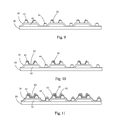
- Step 5 forming an ohmic contact layer on the second metal layer and applying a masking process to form a predetermined pattern so as to form a phosphorous-doped film 52 on the metal electrode (as shown in FIG. 9 ).
- the ohmic contact layer is a phosphorous-doped hydrogenated amorphous silicon (n+a-Si:H) layer, which is formed on the second metal layer through chemical vapor deposition (CVD) and is subjected to operations of coating photoresist, exposure, development, etching, and peeling off photoresist to form a phosphorous-doped (n+) film 52 on the second metal layer.
- CVD chemical vapor deposition
- Step 6 forming a channel layer on the ohmic contact layer and applying a masking process to form a predetermined pattern so as to form an island 62 (as shown in FIG. 10 ).
- the channel layer is a hydrogenated amorphous silicon (a-Si:H) layer, which is formed on the ohmic contact layer chemical vapor deposition (CVD) and is subjected to operations of coating photoresist, exposure, development, etching, and peeling off photoresist to form the island 62 .
- a-Si:H hydrogenated amorphous silicon
- Step 7 forming a gate insulation layer 70 on the channel layer, forming a third metal layer on the gate insulation layer 70 , and applying a masking process to form a predetermined pattern so as to form a gate terminal 82 and a storage capacitor counter electrode, the storage capacitor counter electrode being arranged at an edge location of the black matrix 22 (as shown in FIG. 11 ).
- the gate insulation layer 70 is a silicon nitride (SiNx) layer, which is formed on the channel layer through chemical vapor deposition.
- the gate insulation layer 7 is a gate insulation layer (GI-SiNx).
- the third metal layer is a molybdenum layer, aluminum layer, or a combination of molybdenum layer and aluminum layer, which is formed on the gate insulation layer 70 through sputtering.
- the specific structure of the third metal layer can be adjusted according to the contact of material.
- the third metal layer is of a three layer structure of molybdenum layer, aluminum layer, and molybdenum layer.
- the storage capacitor can be among the first, second, and third metal layers and may alternatively be formed among the first and second metal layers and the transparent conductive layer.
- the storage capacitor is formed among the first and second metal layers and the third metal layer.
- the storage capacitor is set at an edge location of the black matrix 22 in order to increase the aperture rate of the liquid crystal display panel.
- Step 8 forming a protection layer 90 on the third metal layer (as shown in FIG. 13 ).
- the protection layer 90 is a SiNx layer.
- Step 9 forming R, G, B pixels 102 , 104 , 106 on the protection layer 90 (as shown in FIG. 14 ).
- the R, G, B pixels 102 , 104 , 106 are formed on the protection layer 90 through coating operation.
- Step 10 forming vias in locations of the R, G, B pixels 102 , 104 , 106 corresponding to the source terminal 42 and the storage capacitor so as to form holes 108 , the holes 108 being provided for the pixel electrode 112 to be electrically connected to the source terminal 42 and the storage capacitor (as shown in FIG. 15 ).
- Step 11 forming a transparent conductive layer on the R, G, B pixels 102 , 104 , 106 and applying a masking process to form a predetermined pattern so as to form the pixel electrode 112 , thereby forming a COA substrate 200 (as shown in FIG. 16 ).
- the transparent conductive layer is an indium tin oxides (ITO) layer, which is formed through sputtering operation on the R, G, B pixels 102 , 104 , 106 .
- ITO indium tin oxides
- Step 12 bonding the COA substrate 200 to an upper substrate 400 and filling liquid crystal (not shown) between the COA substrate 200 and the upper substrate 400 so as to form a liquid crystal display panel (as shown in FIG. 17 ).
- the first process is to deposit the source terminal, the drain terminal, and the n+ layer simultaneously and then carry out etching.
- the second process is to perform exposure and development of the source terminal and the drain terminal with the black matrix as a mask and to etch off lateral metal in etching the n+ layer.
- the top layer of the gate terminal comprises an n+ layer. If this operation is taken, then the storage capacitor that is of a MIM arrangement is located above the black matrix.
- GI-SiNx that is thinner after the deposition of a-Si:H in Step 6 in order to form a better interface for preventing subsequent interface contamination issue. It is also possible to further deposit a thicker layer of GI-SiNx after the formation of the a-Si:H/GI-SiNx island. Since the interface has already been formed, fast deposition may be used to shorten the deposition time. It may also be possible to use an insulation contact layer of SiO2/Si.
- the present invention provides a method for manufacturing liquid crystal display panel, which greatly simplifies the manufacture of the color filter substrate of the conventional AMLCD. In this way, it only needs to deposit an ITO film on an upper glass substrate. Since there is no black matrix, the ITO film may be of better film formability and can be made flat and having better adherence to glass. Further, since a TFT of top gate structure is adopted, the channel layer can be made thinner and the deposition time is shortened with the electrical property improved and on-state current is increased and off-state current reduced. Compared to COA with bottom gate TFT, this arrangement can simplify the relatively complicated COA operation of one layer glass of TFT substrate, generally due to simplification of TFT operation. Further, since what is finally done is coating of R, G, B, comparatively, the TFT substrate side is flatter. This is favorable to control of liquid crystal in the liquid crystal cell.
Landscapes
- Physics & Mathematics (AREA)
- Nonlinear Science (AREA)
- Engineering & Computer Science (AREA)
- Microelectronics & Electronic Packaging (AREA)
- Mathematical Physics (AREA)
- Chemical & Material Sciences (AREA)
- Crystallography & Structural Chemistry (AREA)
- General Physics & Mathematics (AREA)
- Optics & Photonics (AREA)
- Liquid Crystal (AREA)
- Thin Film Transistor (AREA)
Abstract
Description
Claims (11)
Applications Claiming Priority (3)
| Application Number | Priority Date | Filing Date | Title |
|---|---|---|---|
| CN201210330288.XA CN102799014B (en) | 2012-09-07 | 2012-09-07 | Method for producing liquid crystal display panel |
| CN201210330288 | 2012-09-07 | ||
| PCT/CN2012/081370 WO2014036753A1 (en) | 2012-09-07 | 2012-09-14 | Method of fabricating liquid crystal display panel |
Publications (1)
| Publication Number | Publication Date |
|---|---|
| US8518729B1 true US8518729B1 (en) | 2013-08-27 |
Family
ID=48999708
Family Applications (1)
| Application Number | Title | Priority Date | Filing Date |
|---|---|---|---|
| US13/698,073 Expired - Fee Related US8518729B1 (en) | 2012-09-07 | 2012-09-14 | Method for manufacturing liquid crystal display panel |
Country Status (1)
| Country | Link |
|---|---|
| US (1) | US8518729B1 (en) |
Cited By (3)
| Publication number | Priority date | Publication date | Assignee | Title |
|---|---|---|---|---|
| US20160313600A1 (en) * | 2015-04-24 | 2016-10-27 | Samsung Display Co., Ltd. | Display device having improved transmittance characteristics |
| US9552114B2 (en) * | 2014-12-30 | 2017-01-24 | Shenzhen China Star Optoelectronics Technology Co., Ltd | Touch panel |
| US10120246B2 (en) * | 2016-08-23 | 2018-11-06 | Shenzhen China Star Optoelectronics Technology Co., Ltd. | Manufacturing method of IPS array substrate and IPS array substrate |
Citations (1)
| Publication number | Priority date | Publication date | Assignee | Title |
|---|---|---|---|---|
| US20120068202A1 (en) * | 2009-03-23 | 2012-03-22 | Seiko Epson Corporation | Active matrix substrate, method of manufacturing the same and display equipment using active matrix substrate manufactured by the same method |
-
2012
- 2012-09-14 US US13/698,073 patent/US8518729B1/en not_active Expired - Fee Related
Patent Citations (1)
| Publication number | Priority date | Publication date | Assignee | Title |
|---|---|---|---|---|
| US20120068202A1 (en) * | 2009-03-23 | 2012-03-22 | Seiko Epson Corporation | Active matrix substrate, method of manufacturing the same and display equipment using active matrix substrate manufactured by the same method |
Cited By (4)
| Publication number | Priority date | Publication date | Assignee | Title |
|---|---|---|---|---|
| US9552114B2 (en) * | 2014-12-30 | 2017-01-24 | Shenzhen China Star Optoelectronics Technology Co., Ltd | Touch panel |
| US20160313600A1 (en) * | 2015-04-24 | 2016-10-27 | Samsung Display Co., Ltd. | Display device having improved transmittance characteristics |
| US10012859B2 (en) * | 2015-04-24 | 2018-07-03 | Samsung Display Co., Ltd. | Display device having improved transmittance characteristics |
| US10120246B2 (en) * | 2016-08-23 | 2018-11-06 | Shenzhen China Star Optoelectronics Technology Co., Ltd. | Manufacturing method of IPS array substrate and IPS array substrate |
Similar Documents
| Publication | Publication Date | Title |
|---|---|---|
| EP2782153B1 (en) | Display device, thin film transistor, array substrate and manufacturing method thereof | |
| US10303021B2 (en) | BOA liquid crystal display panel and manufacturing method thereof | |
| US9897880B2 (en) | Array substrate and manufacturing method thereof and liquid crystal display panel using the array substrate | |
| US10120247B2 (en) | Manufacturing method for TFT substrate and TFT substrate manufactured by the manufacturing method thereof | |
| US10355029B2 (en) | Switching element, manufacturing method thereof, array substrate and display device | |
| CN102799014B (en) | Method for producing liquid crystal display panel | |
| US9385141B2 (en) | Array substrate, display panel and method for manufacturing array substrate | |
| US20170153519A1 (en) | Manufacture method of color filter on array liquid crystal display panel and structure thereof | |
| KR101398094B1 (en) | Liquid crystal display and array substrate | |
| US20020180900A1 (en) | Forming method of liquid crystal layer using ink jet system | |
| US20100140623A1 (en) | Array substrate for display device and method of fabricating the same | |
| US20090185120A1 (en) | Thin film transistor substrate and method for manufacturing the same | |
| CN103178119B (en) | Array base palte, array base palte preparation method and display unit | |
| WO2011158424A1 (en) | Thin film transistor substrate and liquid crystal display device | |
| GB2530223B (en) | Method for manufacturing thin-film transistor array substrate | |
| US9281325B2 (en) | Array substrate, manufacturing method thereof and display device | |
| US8518729B1 (en) | Method for manufacturing liquid crystal display panel | |
| US20140252343A1 (en) | Thin-film transistor active device and method for manufacturing same | |
| US8865517B2 (en) | Method for manufacturing thin-film transistor active device and thin-film transistor active device manufactured with same | |
| KR20140145845A (en) | Liquid crystal display device and method of manufacturing the same | |
| KR101747721B1 (en) | Liquid crystal display device and manufacturing method thereof | |
| KR20050105422A (en) | Liquid crystal display panel and fabricating method thereof | |
| US10461102B2 (en) | Display device, transflective array substrate, and manufacturing method thereof | |
| US20140071362A1 (en) | Liquid crystal display panel | |
| KR20080048606A (en) | Thin film transistor substrate and manufacturing method thereof |
Legal Events
| Date | Code | Title | Description |
|---|---|---|---|
| AS | Assignment |
Owner name: S, CHINA Free format text: ASSIGNMENT OF ASSIGNORS INTEREST;ASSIGNOR:DAI, CHAO;REEL/FRAME:029301/0295 Effective date: 20121018 |
|
| STCF | Information on status: patent grant |
Free format text: PATENTED CASE |
|
| FEPP | Fee payment procedure |
Free format text: PAYOR NUMBER ASSIGNED (ORIGINAL EVENT CODE: ASPN); ENTITY STATUS OF PATENT OWNER: LARGE ENTITY |
|
| FPAY | Fee payment |
Year of fee payment: 4 |
|
| MAFP | Maintenance fee payment |
Free format text: PAYMENT OF MAINTENANCE FEE, 8TH YEAR, LARGE ENTITY (ORIGINAL EVENT CODE: M1552); ENTITY STATUS OF PATENT OWNER: LARGE ENTITY Year of fee payment: 8 |
|
| FEPP | Fee payment procedure |
Free format text: MAINTENANCE FEE REMINDER MAILED (ORIGINAL EVENT CODE: REM.); ENTITY STATUS OF PATENT OWNER: LARGE ENTITY |
|
| LAPS | Lapse for failure to pay maintenance fees |
Free format text: PATENT EXPIRED FOR FAILURE TO PAY MAINTENANCE FEES (ORIGINAL EVENT CODE: EXP.); ENTITY STATUS OF PATENT OWNER: LARGE ENTITY |
|
| STCH | Information on status: patent discontinuation |
Free format text: PATENT EXPIRED DUE TO NONPAYMENT OF MAINTENANCE FEES UNDER 37 CFR 1.362 |
|
| FP | Lapsed due to failure to pay maintenance fee |
Effective date: 20250827 |