US8513790B2 - Package-base structure of luminescent diode - Google Patents
Package-base structure of luminescent diode Download PDFInfo
- Publication number
- US8513790B2 US8513790B2 US12/428,342 US42834209A US8513790B2 US 8513790 B2 US8513790 B2 US 8513790B2 US 42834209 A US42834209 A US 42834209A US 8513790 B2 US8513790 B2 US 8513790B2
- Authority
- US
- United States
- Prior art keywords
- conductive layer
- package base
- substrate
- luminescent diode
- insulating layer
- Prior art date
- Legal status (The legal status is an assumption and is not a legal conclusion. Google has not performed a legal analysis and makes no representation as to the accuracy of the status listed.)
- Expired - Fee Related, expires
Links
Images


Classifications
-
- H—ELECTRICITY
- H10—SEMICONDUCTOR DEVICES; ELECTRIC SOLID-STATE DEVICES NOT OTHERWISE PROVIDED FOR
- H10H—INORGANIC LIGHT-EMITTING SEMICONDUCTOR DEVICES HAVING POTENTIAL BARRIERS
- H10H20/00—Individual inorganic light-emitting semiconductor devices having potential barriers, e.g. light-emitting diodes [LED]
- H10H20/80—Constructional details
- H10H20/85—Packages
- H10H20/857—Interconnections, e.g. lead-frames, bond wires or solder balls
-
- H—ELECTRICITY
- H10—SEMICONDUCTOR DEVICES; ELECTRIC SOLID-STATE DEVICES NOT OTHERWISE PROVIDED FOR
- H10H—INORGANIC LIGHT-EMITTING SEMICONDUCTOR DEVICES HAVING POTENTIAL BARRIERS
- H10H20/00—Individual inorganic light-emitting semiconductor devices having potential barriers, e.g. light-emitting diodes [LED]
- H10H20/80—Constructional details
- H10H20/85—Packages
- H10H20/8506—Containers
-
- H—ELECTRICITY
- H10—SEMICONDUCTOR DEVICES; ELECTRIC SOLID-STATE DEVICES NOT OTHERWISE PROVIDED FOR
- H10H—INORGANIC LIGHT-EMITTING SEMICONDUCTOR DEVICES HAVING POTENTIAL BARRIERS
- H10H20/00—Individual inorganic light-emitting semiconductor devices having potential barriers, e.g. light-emitting diodes [LED]
- H10H20/80—Constructional details
- H10H20/85—Packages
- H10H20/858—Means for heat extraction or cooling
- H10H20/8582—Means for heat extraction or cooling characterised by their shape
-
- H—ELECTRICITY
- H10—SEMICONDUCTOR DEVICES; ELECTRIC SOLID-STATE DEVICES NOT OTHERWISE PROVIDED FOR
- H10W—GENERIC PACKAGES, INTERCONNECTIONS, CONNECTORS OR OTHER CONSTRUCTIONAL DETAILS OF DEVICES COVERED BY CLASS H10
- H10W90/00—Package configurations
- H10W90/701—Package configurations characterised by the relative positions of pads or connectors relative to package parts
- H10W90/751—Package configurations characterised by the relative positions of pads or connectors relative to package parts of bond wires
- H10W90/754—Package configurations characterised by the relative positions of pads or connectors relative to package parts of bond wires between a chip and a stacked insulating package substrate, interposer or RDL
Definitions
- the present invention relates to a package base of a luminescent diode, and more particularly to a package base having separate current flow pathway and heat flow pathway.
- the present invention also relates to a process of fabricating such package base.
- Luminescent diode is a semiconductor diode capable of emitting light and serving as a light source.
- Light-emitting diode (LED) and laser diode are typical examples of luminescent diodes.
- the advantages of luminescent diodes over traditional light sources include lower energy consumption, longer lifetime, improved robustness, smaller size and faster switching.
- Luminescent diode is usually packaged before being incorporated into a circuit.
- FIG. 1 a cross-sectional view illustrating a conventional LED package.
- the LED package 10 includes a heat-dissipating substrate 102 , a conductive layer 103 , an insulating layer 104 , a package base 105 and a conducting structure 106 .
- the package base 105 is mounted on the insulating layer 104 and has a holding space 1051 supporting a LED chip 101 .
- the conductive layer 103 serves as a positive electrode 1031 and a negative electrode 1031 , separated by the insulating layer 104 .
- the conducting structure 106 is formed through the package base 105 and the insulating layer 104 so as to be electrically connected to the conductive layer 103 .
- the LED chip 101 can be electrically connected to the positive electrode 1031 and the negative electrode 1032 and receive electricity via external wires 108 .
- An alternative mounting technology, flip chip procedure, can be applied to electrically connect the LED chip 101 to the conducting structure 106 via solder bumps (not shown).
- the heat-dissipating substrate 102 includes a heat conductive layer 1021 and an insulating layer 1022 .
- the insulating layer 1022 is made of heat conductive polymer while the heat conductive layer 1021 is usually made of metal material.
- the insulating layer 1022 interfaced between the heat conductive layer 1021 and the electrodes 1031 and 1032 .
- Such structure makes the heat generated by the LED chip 101 to be dissipated via the heat-dissipating substrate 102 .
- some conductive adhesive (denoted by “A”) may be applied to an area around the conducting structure 106 between the package base 105 and the conductive layer 103 to firmly fix the package base 105 . This increases the area of the heat flow so as to decrease the thermal resistance.
- the present invention provides a package base of a luminescent diode having separate current flow pathway and heat flow pathway so as to prevent the couple thermal-electrical effect on the conductive electrodes.
- the present invention also provides a fabricating process to manufacture a package base having separate current flow pathway and heat flow pathway.
- the package base includes a substrate; a holding space formed on a first surface of the substrate; an insulating layer extending from the holding space to a second surface of the substrate; and a through hole penetrating the insulating layer without touching the substrate.
- the electrode is coated on the surface of the insulating layer.
- a first heat conductive layer is disposed between the luminescent and the substrate.
- a second heat conductive layer is disposed on the second surface of the substrate. The heat flow pathway extending from the first heat conductive layer to the second heat conductive layer is separated from the current flow pathway by the insulating layer.
- the insulating layer includes a porous silicon oxide layer.
- the fabricating process includes the following steps. At first, a holding space having a bottom surface is formed on a first surface of a substrate. Then, a first mask layer is formed on the first surface and an inner surface of the holding space and a second mask layer is formed on a second surface of the substrate. The first mask layer and the second mask layer are patterned to define a first opening and a second opening, respectively. The first opening is located in the holding space. The insulating layer is formed by anodically etching the substrate through the first opening and the second opening to form a porous structure extending from the bottom surface of the holding space to the second surface.
- the second opening has a cross-sectional area larger then that of the first opening.
- FIG. 1 is a cross-sectional view illustrating a conventional LED package
- FIG. 2A is a cross-sectional view illustrating a first preferred embodiment of a package base according to the present invention
- FIG. 2B is a bottom view of the package base of FIG. 2A ;
- FIG. 2C is the cross-sectional view of the package base of FIG. 2A with marked current flow pathway and heat flow pathway;
- FIGS. 3A ⁇ 3L are schematic diagrams illustrating the process of fabricating the package base of FIG. 2A according to the present invention.
- FIG. 4A is a cross-sectional view illustrating a second preferred embodiment of a package base according to the present invention.
- FIG. 4B is a bottom view of the package base of FIG. 4A ;
- FIG. 4C is the cross-sectional view of the package base of FIG. 4A with marked current flow pathway and heat flow pathway;
- FIGS. 5A and 5B illustrate the layout of the package base of FIG. 2A and FIG. 4A in a wafer.
- FIG. 2A is a cross-sectional view illustrating a first preferred embodiment of a package base according to the present invention.
- the cross-sectional view is obtained along the dashed line S-S in FIG. 2B , a bottom view of the package base 2 .
- some layers, for example conductive layer, of the package base 2 are omitted in FIG. 2B to clearly show the essential parts to be described, but the layers not shown in FIG. 2B still exist in the package base 2 .
- the article “a” or “an” may be used for some elements, but the number of the elements is not limited to “one”.
- the package base 2 includes a substrate 20 , a holding space 21 , a through hole 22 and an insulating layer 23 .
- the substrate 20 may be a silicon substrate and has two opposite surfaces 201 and 202 (called first surface 201 and second surface 202 hereinafter).
- the holding space 21 is a cavity arranged at the first surface 201 and has a flat bottom 210 for supporting the luminescent diode 200 .
- the through hole 22 is formed between the flat bottom 210 and the second surface 202 .
- the insulating layer 23 covers a portion of the second surface 202 and the surface of the through hole 22 .
- the insulating layer 23 is made of porous silicon oxide and the formation thereof has been described in U.S. Pat. No. 3,640,806 and No. 3,962,052.
- a conductive layer 24 made of metal or alloy such as TiW/Cu/Ni/Au, Ti/Cu/Ni/Au, Ti/Au/Ni/Au, AlCu/Ni/Au and AuSn, is formed over the insulating layer 23 .
- the luminescent diode 200 is electrically connected to the conductive layer 24 via a wire 27 .
- the luminescent diode 200 may be electrically connected to the conductive layer 24 by flip chip mounting technology. Please note that the arrangement of the positive electrode and the negative electrode varies with the pattern design of the package base and does not described verbosely.
- a first heat conductive layer is interfaced between the luminescent diode 200 and the substrate 20 to conduct the heat generated by the luminescent diode 200 to the substrate 20 .
- a second heat conductive layer is attached to the second surface 202 of the substrate 20 to conduct heat from the substrate 20 out.
- the heat conductive layers 25 and 26 are formed of heat conductive material such as aluminum.
- the current flow pathways A and A′ extend along the conductive layer 24 coated inside the through hole 22 .
- the heat flow pathway B extends along a direction from the first heat conductive layer 25 to the second heat conductive layer 26 .
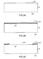
- FIG. 3A ⁇ 3L are schematic diagrams illustrating the process of fabricating such package base of FIG. 2A .
- a substrate 20 for example silicon substrate, having two opposite surfaces 201 and 202 is provided ( FIG. 3A ).
- a mask layer 2011 made of silicon nitride, silicon oxide or metal
- a photoresist layer 2111 are formed on the first surface 201 of the substrate 20 ( FIG. 3B ).
- the mask layer 2011 is patterned by a photolithography and etching procedure to define a first opening 203 ( FIG. 3C ).
- an etching procedure is performed to partially etch off the substrate 20 through the first opening 203 to form the holding space 21 having a flat bottom 210 ( FIG. 3D ).
- the etching procedure is a wet etching procedure or a reactive ion procedure. After removing the remaining photoresist layer 2111 and mask layer 2011 , the resulting structure is shown in FIG. 3E .
- three areas are defined on the substrate 20 . They are the chip area for supporting the luminescent diode chip 200 , the edge area where the package base 2 will be diced after the fabricating process, and the intermediate area between the two areas.
- a mask layer 2012 and a photoresist layer 2112 are formed on the first surface 201 and the surface of the holding space 21 , while another mask layer 2013 and another photoresist layer 2113 are formed on the second surface 202 ( FIG. 3F ).
- the mask layers 2012 and 2013 are patterned by a photolithography and etching procedure to define a second opening 204 and a third opening 205 ( FIG. 3G ).
- the second opening 204 is arranged over a portion of the intermediate area while the third opening 205 is arranged over the edge area and the intermediate area.
- an anodic etching procedure is performed through the second opening 204 and the third opening 205 to form porous silicon oxide, i.e.
- the isolating layer 23 extends from the flat bottom 210 of the holding space 21 to the second surface 202 of the substrate 20 . In this cross-sectional view, it is shown that a L-shaped insulating layer 23 is formed adjacent to the chip area.
- the anodic etching step is performed in a HF solution.
- Another insulating layer 231 may be formed on the first surface 201 in the edge area by defining a fourth opening 206 and anodically etching the substrate 20 through the fourth opening 206 . Since the insulating layer 231 whose material is almost porous silicon oxide can be controllably etched by BOE etching, the dicing after the fabrication of the package base becomes easier.
- a spacer 2014 is formed on the surface of the second opening 204 , and a protective layer 2015 is also formed on the insulating layer 231 to prevent the insulating layer 231 from being etched in the following step ( FIG. 3I ).
- a through hole 22 is formed in the insulating layer 23 and penetrates the substrate 20 ( FIG. 3J ).
- the resulting structure is shown in FIG. 3K .
- a conductive layer 24 is formed to cover the isolating layer 23 .
- a first heat conductive layer 25 and a second heat conductive layer 26 are formed at the opposite sides of the substrate 20 in the chip area ( FIG. 3L ).
- the resulting structure i.e. the package base, is ready for the mounting of the luminescent diode chip.
- a luminescent diode chip is electrically connected to the conductive layer 24 to get the structure as shown in FIG. 2A .
- an impurity may be shallowly introduced through the openings 204 , 205 and 206 into the substrate 20 to form low resistivity regions.
- the impurity is introduced by diffusion or ion implantation.
- the low resistivity regions have a thickness ranging from 1 ⁇ 10 ⁇ m.
- FIG. 4A illustrates a second preferred embodiment of a package base according to the present invention.
- the cross-sectional view is obtained along the dashed line S′-S′ in FIG. 4B , a bottom view of the package base 3 .
- some layers, for example conductive layer, of the package base 3 are omitted in FIG. 4B to clearly show the essential parts to be described, but the layers not shown in FIG. 4B still exist in the package base 3 .
- the package base 3 includes a substrate 30 , a holding space 31 , a through hole 32 , an insulating layer 33 , a conductive layer 34 and two heat conductive layers 35 and 36 , which are similar to those described with reference to FIG. 2A .
- a further heat conductive layer 38 is formed to provide a further heat flow pathway.
- the insulating layer 33 in the intermediate area is shortened to provide a space for the heat conductive layer 38 .
- the third opening 205 in FIG. 3G defined by the mask layer 2013 is arranged over the edge area and only a portion of the intermediate area.
- the second surface 302 of the substrate 30 in the other portion of the intermediate area is not affected so that the insulating lager 33 does not cover the other portion of the intermediate area.
- the heat conductive layer 38 is formed together with the second heat conductive layer 36 .
- the other steps of fabricating the package base 3 are similar to those described with reference to FIGS. 3A ⁇ 3L and do not described verbosely.
- FIG. 4C illustrates the current flow pathway and the heat flow pathway of the package base according to the present invention.
- the current flow pathways A and A′ extend along the conductive layer 34 coated inside the through hole 32 .
- the heat flow pathway B extends along a direction from the first heat conductive layer 35 to the second heat conductive layer 36 .
- Another heat flow pathways C and C′ extend along a direction from the luminescent diode chip 300 to the heat conductive layer 38 through the intermediate area of the substrate 30 .
- the wafer After the fabricating process, there are a plurality of dies formed in the wafer.
- the layout is arranged as shown in FIG. 5A and FIG. 5B . Although only four dies are shown, in fact, there are hundreds of dies formed in the wafer.
- the wafer should be diced into unit dies, each of which has the package base structure of FIG. 2A or FIG. 4A .
- the wafer can be easily cut along the porous silicon by BOE etching.
- the luminescent diode package base of the present invention has separate current flow pathway and heat flow pathway.
- An insulating layer is formed between the current flow pathway and the heat flow pathway to prevent the “mixing” of them. Hence, the annoying coupled thermal-electrical effect does not occur so as to ensure the long lifetime of the luminescent diode package.
Landscapes
- Led Device Packages (AREA)
Abstract
Description
Claims (13)
Applications Claiming Priority (3)
| Application Number | Priority Date | Filing Date | Title |
|---|---|---|---|
| TW097114723 | 2008-04-22 | ||
| TW097114723A TWI351777B (en) | 2008-04-22 | 2008-04-22 | Bade for light diode and its manufacturing method |
| TW97114723A | 2008-04-22 |
Publications (2)
| Publication Number | Publication Date |
|---|---|
| US20090261375A1 US20090261375A1 (en) | 2009-10-22 |
| US8513790B2 true US8513790B2 (en) | 2013-08-20 |
Family
ID=41200378
Family Applications (1)
| Application Number | Title | Priority Date | Filing Date |
|---|---|---|---|
| US12/428,342 Expired - Fee Related US8513790B2 (en) | 2008-04-22 | 2009-04-22 | Package-base structure of luminescent diode |
Country Status (2)
| Country | Link |
|---|---|
| US (1) | US8513790B2 (en) |
| TW (1) | TWI351777B (en) |
Cited By (5)
| Publication number | Priority date | Publication date | Assignee | Title |
|---|---|---|---|---|
| US11156346B2 (en) * | 2019-11-19 | 2021-10-26 | Lumileds Llc | Fan out structure for light-emitting diode (LED) device and lighting system |
| US11476217B2 (en) | 2020-03-10 | 2022-10-18 | Lumileds Llc | Method of manufacturing an augmented LED array assembly |
| US11610935B2 (en) | 2019-03-29 | 2023-03-21 | Lumileds Llc | Fan-out light-emitting diode (LED) device substrate with embedded backplane, lighting system and method of manufacture |
| US11664347B2 (en) | 2020-01-07 | 2023-05-30 | Lumileds Llc | Ceramic carrier and build up carrier for light-emitting diode (LED) array |
| US11777066B2 (en) | 2019-12-27 | 2023-10-03 | Lumileds Llc | Flipchip interconnected light-emitting diode package assembly |
Families Citing this family (8)
| Publication number | Priority date | Publication date | Assignee | Title |
|---|---|---|---|---|
| US8044412B2 (en) | 2006-01-20 | 2011-10-25 | Taiwan Semiconductor Manufacturing Company, Ltd | Package for a light emitting element |
| US10290788B2 (en) * | 2009-11-24 | 2019-05-14 | Luminus Devices, Inc. | Systems and methods for managing heat from an LED |
| US9293678B2 (en) | 2010-07-15 | 2016-03-22 | Micron Technology, Inc. | Solid-state light emitters having substrates with thermal and electrical conductivity enhancements and method of manufacture |
| TWI442496B (en) * | 2011-03-01 | 2014-06-21 | 隆達電子股份有限公司 | Optical machine module and manufacturing method thereof |
| DE102012216546B4 (en) * | 2012-09-17 | 2023-01-19 | Infineon Technologies Ag | METHOD OF SOLDERING A SEMICONDUCTOR CHIP TO A CARRIER |
| TW201532327A (en) * | 2013-11-19 | 2015-08-16 | 威廉馬許萊斯大學 | Porous SiOx material for improving the effectiveness of SiOx switching elements |
| DE102018131954A1 (en) | 2018-12-12 | 2020-06-18 | Osram Opto Semiconductors Gmbh | CARRIER, ARRANGEMENT WITH A CARRIER, AND METHOD FOR PRODUCING A CARRIER |
| US11189771B2 (en) * | 2019-12-11 | 2021-11-30 | Mikro Mesa Technology Co., Ltd. | Breathable micro light emitting diode display |
Citations (10)
| Publication number | Priority date | Publication date | Assignee | Title |
|---|---|---|---|---|
| US3640806A (en) | 1970-01-05 | 1972-02-08 | Nippon Telegraph & Telephone | Semiconductor device and method of producing the same |
| US3962052A (en) | 1975-04-14 | 1976-06-08 | International Business Machines Corporation | Process for forming apertures in silicon bodies |
| US6443597B1 (en) | 1999-09-01 | 2002-09-03 | Sony Corporation | Plane display unit and plane display device |
| US20030160327A1 (en) * | 2002-02-28 | 2003-08-28 | Kabushiki Kaisha Toshiba | Semiconductor device |
| US20040075100A1 (en) | 2001-04-10 | 2004-04-22 | Georg Bogner | Leadframe and housing for radiation-emitting component, radiation-emitting component, and a method for producing the component |
| US20050205974A1 (en) | 2004-03-19 | 2005-09-22 | Hung-Yuan Su | Optoelectronic semiconductor component |
| US6953952B2 (en) | 2002-09-05 | 2005-10-11 | Nichia Corporation | Semiconductor device and an optical device using the semiconductor device |
| US20060023451A1 (en) | 2004-07-28 | 2006-02-02 | Samsung Electro-Mechanics Co., Ltd. | LED package for backlight unit |
| US20060055050A1 (en) * | 2004-09-10 | 2006-03-16 | Hideo Numata | Semiconductor device and manufacturing method thereof |
| US20080017962A1 (en) * | 2006-07-24 | 2008-01-24 | Hung-Yi Lin | Si-substrate and structure of opto-electronic package having the same |
-
2008
- 2008-04-22 TW TW097114723A patent/TWI351777B/en active
-
2009
- 2009-04-22 US US12/428,342 patent/US8513790B2/en not_active Expired - Fee Related
Patent Citations (10)
| Publication number | Priority date | Publication date | Assignee | Title |
|---|---|---|---|---|
| US3640806A (en) | 1970-01-05 | 1972-02-08 | Nippon Telegraph & Telephone | Semiconductor device and method of producing the same |
| US3962052A (en) | 1975-04-14 | 1976-06-08 | International Business Machines Corporation | Process for forming apertures in silicon bodies |
| US6443597B1 (en) | 1999-09-01 | 2002-09-03 | Sony Corporation | Plane display unit and plane display device |
| US20040075100A1 (en) | 2001-04-10 | 2004-04-22 | Georg Bogner | Leadframe and housing for radiation-emitting component, radiation-emitting component, and a method for producing the component |
| US20030160327A1 (en) * | 2002-02-28 | 2003-08-28 | Kabushiki Kaisha Toshiba | Semiconductor device |
| US6953952B2 (en) | 2002-09-05 | 2005-10-11 | Nichia Corporation | Semiconductor device and an optical device using the semiconductor device |
| US20050205974A1 (en) | 2004-03-19 | 2005-09-22 | Hung-Yuan Su | Optoelectronic semiconductor component |
| US20060023451A1 (en) | 2004-07-28 | 2006-02-02 | Samsung Electro-Mechanics Co., Ltd. | LED package for backlight unit |
| US20060055050A1 (en) * | 2004-09-10 | 2006-03-16 | Hideo Numata | Semiconductor device and manufacturing method thereof |
| US20080017962A1 (en) * | 2006-07-24 | 2008-01-24 | Hung-Yi Lin | Si-substrate and structure of opto-electronic package having the same |
Cited By (10)
| Publication number | Priority date | Publication date | Assignee | Title |
|---|---|---|---|---|
| US11610935B2 (en) | 2019-03-29 | 2023-03-21 | Lumileds Llc | Fan-out light-emitting diode (LED) device substrate with embedded backplane, lighting system and method of manufacture |
| US11626448B2 (en) | 2019-03-29 | 2023-04-11 | Lumileds Llc | Fan-out light-emitting diode (LED) device substrate with embedded backplane, lighting system and method of manufacture |
| US11156346B2 (en) * | 2019-11-19 | 2021-10-26 | Lumileds Llc | Fan out structure for light-emitting diode (LED) device and lighting system |
| US11621173B2 (en) | 2019-11-19 | 2023-04-04 | Lumileds Llc | Fan out structure for light-emitting diode (LED) device and lighting system |
| US11631594B2 (en) | 2019-11-19 | 2023-04-18 | Lumileds Llc | Fan out structure for light-emitting diode (LED) device and lighting system |
| US12224182B2 (en) | 2019-11-19 | 2025-02-11 | Lumileds, LLC | Fan out structure for light-emitting diode (LED) device and lighting system |
| US11777066B2 (en) | 2019-12-27 | 2023-10-03 | Lumileds Llc | Flipchip interconnected light-emitting diode package assembly |
| US11664347B2 (en) | 2020-01-07 | 2023-05-30 | Lumileds Llc | Ceramic carrier and build up carrier for light-emitting diode (LED) array |
| US12191280B2 (en) | 2020-01-07 | 2025-01-07 | Lumileds, LLC | Ceramic carrier and build up carrier for light-emitting diode (LED) array |
| US11476217B2 (en) | 2020-03-10 | 2022-10-18 | Lumileds Llc | Method of manufacturing an augmented LED array assembly |
Also Published As
| Publication number | Publication date |
|---|---|
| US20090261375A1 (en) | 2009-10-22 |
| TW200945616A (en) | 2009-11-01 |
| TWI351777B (en) | 2011-11-01 |
Similar Documents
| Publication | Publication Date | Title |
|---|---|---|
| US8513790B2 (en) | Package-base structure of luminescent diode | |
| CN102637784B (en) | Light-emitting diode packaging substrate and manufacturing method thereof | |
| JP5378130B2 (en) | Semiconductor light emitting device | |
| TWI429108B (en) | Semiconductor light emitting device | |
| JP6023660B2 (en) | Semiconductor light emitting device and semiconductor light emitting device | |
| CN101889354B (en) | Light emitting device package and manufacturing method thereof | |
| TWI595686B (en) | Semiconductor light-emitting device | |
| TWI612696B (en) | Light-emitting diode (LED) structure and method of forming a flip-chip LED structure | |
| EP2244309A1 (en) | Led package structure having the led and method for fabricating the led | |
| US7892870B2 (en) | Thermal management for LED | |
| JP5148336B2 (en) | Light emitting diode chip and manufacturing method thereof | |
| CN111446343B (en) | A semiconductor light-emitting device | |
| JP2013232478A (en) | Semiconductor light-emitting device and method of manufacturing the same | |
| JP2010219377A (en) | Semiconductor light-emitting device and method of manufacturing the same | |
| JP2013201253A (en) | Semiconductor light emitting element and manufacturing method of the same | |
| JP2012174902A (en) | Method of manufacturing nitride semiconductor light-emitting element | |
| US20100213810A1 (en) | Light emitting device package | |
| JP2017054902A (en) | Semiconductor light emitting device | |
| CN102456783B (en) | Ultraviolet light emitting diode chip with vertical structure and manufacture method thereof | |
| US20240421278A1 (en) | Semiconductor light emitting device and method for manufacturing the same | |
| JP2001085750A (en) | Nitride semiconductor light-emitting chip | |
| JP2017055045A (en) | Semiconductor light emitting device | |
| JP5148337B2 (en) | Light emitting diode chip and manufacturing method thereof | |
| US20190006310A1 (en) | Mounting component, semiconductor device using same, and manufacturing method thereof | |
| KR101348405B1 (en) | Packaging of light emitting diode using silicon wafer and manufacturing method of the same |
Legal Events
| Date | Code | Title | Description |
|---|---|---|---|
| AS | Assignment |
Owner name: SILICON BASE DEVELOPMENT INC., TAIWAN Free format text: ASSIGNMENT OF ASSIGNORS INTEREST;ASSIGNORS:CHEN, CHIH-MING;HWANG, DENG-HUEI;CHENG, CHING-CHI;REEL/FRAME:022583/0366 Effective date: 20090422 |
|
| STCF | Information on status: patent grant |
Free format text: PATENTED CASE |
|
| FEPP | Fee payment procedure |
Free format text: PAYOR NUMBER ASSIGNED (ORIGINAL EVENT CODE: ASPN); ENTITY STATUS OF PATENT OWNER: SMALL ENTITY |
|
| FPAY | Fee payment |
Year of fee payment: 4 |
|
| MAFP | Maintenance fee payment |
Free format text: PAYMENT OF MAINTENANCE FEE, 8TH YR, SMALL ENTITY (ORIGINAL EVENT CODE: M2552); ENTITY STATUS OF PATENT OWNER: SMALL ENTITY Year of fee payment: 8 |
|
| FEPP | Fee payment procedure |
Free format text: MAINTENANCE FEE REMINDER MAILED (ORIGINAL EVENT CODE: REM.); ENTITY STATUS OF PATENT OWNER: SMALL ENTITY |
|
| LAPS | Lapse for failure to pay maintenance fees |
Free format text: PATENT EXPIRED FOR FAILURE TO PAY MAINTENANCE FEES (ORIGINAL EVENT CODE: EXP.); ENTITY STATUS OF PATENT OWNER: SMALL ENTITY |
|
| STCH | Information on status: patent discontinuation |
Free format text: PATENT EXPIRED DUE TO NONPAYMENT OF MAINTENANCE FEES UNDER 37 CFR 1.362 |
|
| FP | Lapsed due to failure to pay maintenance fee |
Effective date: 20250820 |