US8466518B2 - Semiconductor device and semiconductor device manufacturing method - Google Patents
Semiconductor device and semiconductor device manufacturing method Download PDFInfo
- Publication number
- US8466518B2 US8466518B2 US13/098,881 US201113098881A US8466518B2 US 8466518 B2 US8466518 B2 US 8466518B2 US 201113098881 A US201113098881 A US 201113098881A US 8466518 B2 US8466518 B2 US 8466518B2
- Authority
- US
- United States
- Prior art keywords
- film
- etching stopper
- etching
- region
- stress
- Prior art date
- Legal status (The legal status is an assumption and is not a legal conclusion. Google has not performed a legal analysis and makes no representation as to the accuracy of the status listed.)
- Expired - Fee Related, expires
Links
- 239000004065 semiconductor Substances 0.000 title claims abstract description 98
- 238000004519 manufacturing process Methods 0.000 title claims abstract description 22
- 238000005530 etching Methods 0.000 claims abstract description 374
- 238000009413 insulation Methods 0.000 claims description 64
- 239000000758 substrate Substances 0.000 claims description 60
- KRHYYFGTRYWZRS-UHFFFAOYSA-N Fluorane Chemical compound F KRHYYFGTRYWZRS-UHFFFAOYSA-N 0.000 claims description 52
- 229910052581 Si3N4 Inorganic materials 0.000 claims description 24
- HQVNEWCFYHHQES-UHFFFAOYSA-N silicon nitride Chemical compound N12[Si]34N5[Si]62N3[Si]51N64 HQVNEWCFYHHQES-UHFFFAOYSA-N 0.000 claims description 24
- OKTJSMMVPCPJKN-UHFFFAOYSA-N Carbon Chemical compound [C] OKTJSMMVPCPJKN-UHFFFAOYSA-N 0.000 claims description 23
- 229910052799 carbon Inorganic materials 0.000 claims description 23
- 238000009792 diffusion process Methods 0.000 claims description 22
- VYPSYNLAJGMNEJ-UHFFFAOYSA-N Silicium dioxide Chemical compound O=[Si]=O VYPSYNLAJGMNEJ-UHFFFAOYSA-N 0.000 claims description 17
- 229910052814 silicon oxide Inorganic materials 0.000 claims description 17
- 229920002120 photoresistant polymer Polymers 0.000 description 63
- 239000010410 layer Substances 0.000 description 45
- 239000011229 interlayer Substances 0.000 description 35
- 239000012535 impurity Substances 0.000 description 27
- 239000002184 metal Substances 0.000 description 17
- 229910052751 metal Inorganic materials 0.000 description 17
- 238000000206 photolithography Methods 0.000 description 17
- 239000002019 doping agent Substances 0.000 description 15
- 229910021332 silicide Inorganic materials 0.000 description 15
- FVBUAEGBCNSCDD-UHFFFAOYSA-N silicide(4-) Chemical compound [Si-4] FVBUAEGBCNSCDD-UHFFFAOYSA-N 0.000 description 15
- 230000004888 barrier function Effects 0.000 description 14
- NBVXSUQYWXRMNV-UHFFFAOYSA-N fluoromethane Chemical compound FC NBVXSUQYWXRMNV-UHFFFAOYSA-N 0.000 description 12
- 238000000034 method Methods 0.000 description 12
- 238000004380 ashing Methods 0.000 description 10
- 238000004528 spin coating Methods 0.000 description 10
- 230000006870 function Effects 0.000 description 9
- 229910021420 polycrystalline silicon Inorganic materials 0.000 description 8
- 229920005591 polysilicon Polymers 0.000 description 8
- PQDJYEQOELDLCP-UHFFFAOYSA-N trimethylsilane Chemical compound C[SiH](C)C PQDJYEQOELDLCP-UHFFFAOYSA-N 0.000 description 8
- 238000002955 isolation Methods 0.000 description 7
- BLRPTPMANUNPDV-UHFFFAOYSA-N Silane Chemical compound [SiH4] BLRPTPMANUNPDV-UHFFFAOYSA-N 0.000 description 6
- 238000005229 chemical vapour deposition Methods 0.000 description 6
- 238000005468 ion implantation Methods 0.000 description 6
- 238000001312 dry etching Methods 0.000 description 5
- 238000000623 plasma-assisted chemical vapour deposition Methods 0.000 description 5
- 239000002994 raw material Substances 0.000 description 5
- 239000003870 refractory metal Substances 0.000 description 5
- XUIMIQQOPSSXEZ-UHFFFAOYSA-N Silicon Chemical compound [Si] XUIMIQQOPSSXEZ-UHFFFAOYSA-N 0.000 description 4
- 239000010949 copper Substances 0.000 description 4
- 230000007423 decrease Effects 0.000 description 4
- 239000000463 material Substances 0.000 description 4
- 239000005360 phosphosilicate glass Substances 0.000 description 4
- 210000002381 plasma Anatomy 0.000 description 4
- 230000005855 radiation Effects 0.000 description 4
- DDFHBQSCUXNBSA-UHFFFAOYSA-N 5-(5-carboxythiophen-2-yl)thiophene-2-carboxylic acid Chemical compound S1C(C(=O)O)=CC=C1C1=CC=C(C(O)=O)S1 DDFHBQSCUXNBSA-UHFFFAOYSA-N 0.000 description 3
- XPDWGBQVDMORPB-UHFFFAOYSA-N Fluoroform Chemical compound FC(F)F XPDWGBQVDMORPB-UHFFFAOYSA-N 0.000 description 3
- ATJFFYVFTNAWJD-UHFFFAOYSA-N Tin Chemical compound [Sn] ATJFFYVFTNAWJD-UHFFFAOYSA-N 0.000 description 3
- 230000015572 biosynthetic process Effects 0.000 description 3
- 239000004020 conductor Substances 0.000 description 3
- 230000002950 deficient Effects 0.000 description 3
- RWRIWBAIICGTTQ-UHFFFAOYSA-N difluoromethane Chemical compound FCF RWRIWBAIICGTTQ-UHFFFAOYSA-N 0.000 description 3
- 230000005279 excitation period Effects 0.000 description 3
- 238000000059 patterning Methods 0.000 description 3
- 238000004544 sputter deposition Methods 0.000 description 3
- PXHVJJICTQNCMI-UHFFFAOYSA-N Nickel Chemical compound [Ni] PXHVJJICTQNCMI-UHFFFAOYSA-N 0.000 description 2
- BOTDANWDWHJENH-UHFFFAOYSA-N Tetraethyl orthosilicate Chemical compound CCO[Si](OCC)(OCC)OCC BOTDANWDWHJENH-UHFFFAOYSA-N 0.000 description 2
- 230000008901 benefit Effects 0.000 description 2
- 239000010941 cobalt Substances 0.000 description 2
- 229910017052 cobalt Inorganic materials 0.000 description 2
- GUTLYIVDDKVIGB-UHFFFAOYSA-N cobalt atom Chemical compound [Co] GUTLYIVDDKVIGB-UHFFFAOYSA-N 0.000 description 2
- 230000000694 effects Effects 0.000 description 2
- 238000009713 electroplating Methods 0.000 description 2
- 239000000203 mixture Substances 0.000 description 2
- 238000005268 plasma chemical vapour deposition Methods 0.000 description 2
- 229910052710 silicon Inorganic materials 0.000 description 2
- 239000010703 silicon Substances 0.000 description 2
- 239000000126 substance Substances 0.000 description 2
- CZDYPVPMEAXLPK-UHFFFAOYSA-N tetramethylsilane Chemical compound C[Si](C)(C)C CZDYPVPMEAXLPK-UHFFFAOYSA-N 0.000 description 2
- WFKWXMTUELFFGS-UHFFFAOYSA-N tungsten Chemical compound [W] WFKWXMTUELFFGS-UHFFFAOYSA-N 0.000 description 2
- 229910052721 tungsten Inorganic materials 0.000 description 2
- 239000010937 tungsten Substances 0.000 description 2
- RYGMFSIKBFXOCR-UHFFFAOYSA-N Copper Chemical compound [Cu] RYGMFSIKBFXOCR-UHFFFAOYSA-N 0.000 description 1
- 229910007159 Si(CH3)4 Inorganic materials 0.000 description 1
- 230000004075 alteration Effects 0.000 description 1
- 229910052802 copper Inorganic materials 0.000 description 1
- 230000003247 decreasing effect Effects 0.000 description 1
- 238000012986 modification Methods 0.000 description 1
- 230000004048 modification Effects 0.000 description 1
- 229910052759 nickel Inorganic materials 0.000 description 1
- 229910021334 nickel silicide Inorganic materials 0.000 description 1
- RUFLMLWJRZAWLJ-UHFFFAOYSA-N nickel silicide Chemical compound [Ni]=[Si]=[Ni] RUFLMLWJRZAWLJ-UHFFFAOYSA-N 0.000 description 1
- 230000008520 organization Effects 0.000 description 1
- 230000003647 oxidation Effects 0.000 description 1
- 238000007254 oxidation reaction Methods 0.000 description 1
- 210000003254 palate Anatomy 0.000 description 1
- 238000005498 polishing Methods 0.000 description 1
- 238000009751 slip forming Methods 0.000 description 1
- 238000006467 substitution reaction Methods 0.000 description 1
- 229910052715 tantalum Inorganic materials 0.000 description 1
- GUVRBAGPIYLISA-UHFFFAOYSA-N tantalum atom Chemical compound [Ta] GUVRBAGPIYLISA-UHFFFAOYSA-N 0.000 description 1
- 238000001039 wet etching Methods 0.000 description 1
Images


Classifications
-
- H—ELECTRICITY
- H01—ELECTRIC ELEMENTS
- H01L—SEMICONDUCTOR DEVICES NOT COVERED BY CLASS H10
- H01L21/00—Processes or apparatus adapted for the manufacture or treatment of semiconductor or solid state devices or of parts thereof
- H01L21/70—Manufacture or treatment of devices consisting of a plurality of solid state components formed in or on a common substrate or of parts thereof; Manufacture of integrated circuit devices or of parts thereof
- H01L21/77—Manufacture or treatment of devices consisting of a plurality of solid state components or integrated circuits formed in, or on, a common substrate
- H01L21/78—Manufacture or treatment of devices consisting of a plurality of solid state components or integrated circuits formed in, or on, a common substrate with subsequent division of the substrate into plural individual devices
- H01L21/82—Manufacture or treatment of devices consisting of a plurality of solid state components or integrated circuits formed in, or on, a common substrate with subsequent division of the substrate into plural individual devices to produce devices, e.g. integrated circuits, each consisting of a plurality of components
- H01L21/822—Manufacture or treatment of devices consisting of a plurality of solid state components or integrated circuits formed in, or on, a common substrate with subsequent division of the substrate into plural individual devices to produce devices, e.g. integrated circuits, each consisting of a plurality of components the substrate being a semiconductor, using silicon technology
- H01L21/8232—Field-effect technology
- H01L21/8234—MIS technology, i.e. integration processes of field effect transistors of the conductor-insulator-semiconductor type
- H01L21/8238—Complementary field-effect transistors, e.g. CMOS
- H01L21/823807—Complementary field-effect transistors, e.g. CMOS with a particular manufacturing method of the channel structures, e.g. channel implants, halo or pocket implants, or channel materials
-
- H—ELECTRICITY
- H01—ELECTRIC ELEMENTS
- H01L—SEMICONDUCTOR DEVICES NOT COVERED BY CLASS H10
- H01L21/00—Processes or apparatus adapted for the manufacture or treatment of semiconductor or solid state devices or of parts thereof
- H01L21/70—Manufacture or treatment of devices consisting of a plurality of solid state components formed in or on a common substrate or of parts thereof; Manufacture of integrated circuit devices or of parts thereof
- H01L21/71—Manufacture of specific parts of devices defined in group H01L21/70
- H01L21/768—Applying interconnections to be used for carrying current between separate components within a device comprising conductors and dielectrics
- H01L21/76801—Applying interconnections to be used for carrying current between separate components within a device comprising conductors and dielectrics characterised by the formation and the after-treatment of the dielectrics, e.g. smoothing
- H01L21/76829—Applying interconnections to be used for carrying current between separate components within a device comprising conductors and dielectrics characterised by the formation and the after-treatment of the dielectrics, e.g. smoothing characterised by the formation of thin functional dielectric layers, e.g. dielectric etch-stop, barrier, capping or liner layers
- H01L21/76832—Multiple layers
-
- H—ELECTRICITY
- H01—ELECTRIC ELEMENTS
- H01L—SEMICONDUCTOR DEVICES NOT COVERED BY CLASS H10
- H01L21/00—Processes or apparatus adapted for the manufacture or treatment of semiconductor or solid state devices or of parts thereof
- H01L21/70—Manufacture or treatment of devices consisting of a plurality of solid state components formed in or on a common substrate or of parts thereof; Manufacture of integrated circuit devices or of parts thereof
- H01L21/77—Manufacture or treatment of devices consisting of a plurality of solid state components or integrated circuits formed in, or on, a common substrate
- H01L21/78—Manufacture or treatment of devices consisting of a plurality of solid state components or integrated circuits formed in, or on, a common substrate with subsequent division of the substrate into plural individual devices
- H01L21/82—Manufacture or treatment of devices consisting of a plurality of solid state components or integrated circuits formed in, or on, a common substrate with subsequent division of the substrate into plural individual devices to produce devices, e.g. integrated circuits, each consisting of a plurality of components
- H01L21/822—Manufacture or treatment of devices consisting of a plurality of solid state components or integrated circuits formed in, or on, a common substrate with subsequent division of the substrate into plural individual devices to produce devices, e.g. integrated circuits, each consisting of a plurality of components the substrate being a semiconductor, using silicon technology
- H01L21/8232—Field-effect technology
- H01L21/8234—MIS technology, i.e. integration processes of field effect transistors of the conductor-insulator-semiconductor type
- H01L21/8238—Complementary field-effect transistors, e.g. CMOS
- H01L21/823871—Complementary field-effect transistors, e.g. CMOS interconnection or wiring or contact manufacturing related aspects
-
- H—ELECTRICITY
- H01—ELECTRIC ELEMENTS
- H01L—SEMICONDUCTOR DEVICES NOT COVERED BY CLASS H10
- H01L23/00—Details of semiconductor or other solid state devices
- H01L23/48—Arrangements for conducting electric current to or from the solid state body in operation, e.g. leads, terminal arrangements ; Selection of materials therefor
- H01L23/482—Arrangements for conducting electric current to or from the solid state body in operation, e.g. leads, terminal arrangements ; Selection of materials therefor consisting of lead-in layers inseparably applied to the semiconductor body
- H01L23/485—Arrangements for conducting electric current to or from the solid state body in operation, e.g. leads, terminal arrangements ; Selection of materials therefor consisting of lead-in layers inseparably applied to the semiconductor body consisting of layered constructions comprising conductive layers and insulating layers, e.g. planar contacts
-
- H—ELECTRICITY
- H01—ELECTRIC ELEMENTS
- H01L—SEMICONDUCTOR DEVICES NOT COVERED BY CLASS H10
- H01L29/00—Semiconductor devices adapted for rectifying, amplifying, oscillating or switching, or capacitors or resistors with at least one potential-jump barrier or surface barrier, e.g. PN junction depletion layer or carrier concentration layer; Details of semiconductor bodies or of electrodes thereof ; Multistep manufacturing processes therefor
- H01L29/66—Types of semiconductor device ; Multistep manufacturing processes therefor
- H01L29/68—Types of semiconductor device ; Multistep manufacturing processes therefor controllable by only the electric current supplied, or only the electric potential applied, to an electrode which does not carry the current to be rectified, amplified or switched
- H01L29/76—Unipolar devices, e.g. field effect transistors
- H01L29/772—Field effect transistors
- H01L29/78—Field effect transistors with field effect produced by an insulated gate
- H01L29/7842—Field effect transistors with field effect produced by an insulated gate means for exerting mechanical stress on the crystal lattice of the channel region, e.g. using a flexible substrate
- H01L29/7843—Field effect transistors with field effect produced by an insulated gate means for exerting mechanical stress on the crystal lattice of the channel region, e.g. using a flexible substrate the means being an applied insulating layer
-
- H—ELECTRICITY
- H01—ELECTRIC ELEMENTS
- H01L—SEMICONDUCTOR DEVICES NOT COVERED BY CLASS H10
- H01L2924/00—Indexing scheme for arrangements or methods for connecting or disconnecting semiconductor or solid-state bodies as covered by H01L24/00
- H01L2924/0001—Technical content checked by a classifier
- H01L2924/0002—Not covered by any one of groups H01L24/00, H01L24/00 and H01L2224/00
Definitions
- the embodiments discussed herein are related to a semiconductor device and a method for manufacturing the semiconductor device.
- CMOS circuit including a PMOS transistor and an NMOS transistor is noted.
- a gate interconnect is formed continuously in a PMOS transistor forming region and in a NMOS transistor forming region.
- a part of the gate interconnect in the PMOS transistor forming region functions as the gate electrode of the PMOS transistor
- a part of the gate interconnect in the NMOS transistor forming region functions as the gate electrode of the NMOS transistor.
- an inter-layer insulation film is formed, covering the PMOS transistor and the NMOS transistor.
- a contact hole is formed down to the gate interconnect.
- an electrically conductive plug is formed in the contact hole.
- an insulation film (compressive stress film) is used, covering the PMOS transistor so that compressive stresses are applied to a channel region of the PMOS transistor.
- an insulation film (tensile stress film) is used, covering the NMOS transistor so that tensile stresses are applied to the channel region of the NMOS transistor.
- a semiconductor device manufacturing method includes forming a gate interconnect both in a first region and a second region of a semiconductor substrate, forming in the first region a first transistor including a first gate electrode which is a part of the gate interconnect, and forming in the second region a second transistor including a second gate electrode which is another part of the gate interconnect; forming over the semiconductor substrate a first stress film so as to cover the first transistor and the second transistor; forming a first etching stopper film over the first stress film; forming over the first etching stopper film a second etching stopper film whose etching characteristic is different from an etching characteristic of the first etching stopper film; forming a first mask layer covering the first region and exposing the second region; removing the second etching stopper film in the second region with the first mask layer as a mask and the first etching stopper film as the stopper, and isotropically etching the second etching stopper film located below the first mask layer;
- a semiconductor device includes a gate interconnect formed both in a first region and a second region of a semiconductor substrate; a first transistor formed in the first region and including a first gate electrode which is a part of the gate interconnect, and first source/drain diffusion layers formed in the semiconductor substrate on both sides of the first gate electrode; a second transistor formed in the second region and including second gate electrode which is another part of the gate interconnect and second source/drain diffusion layers formed in the semiconductor substrate on both side of the second gate electrodes; a first stress film formed over the semiconductor substrate in the first region so as to cover the first transistor; a first etching stopper film formed over the first stress film; a second etching stopper film whose etching characteristic is different from an etching characteristic of the first etching stopper film and formed over the first region except a part thereof near the second region; a second stress film formed over the semiconductor substrate in the second region so as to cover the second transistor, an edge of the second stress film on the side of the first region being overlap
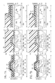
- FIG. 1 is a sectional view of a semiconductor device according to one embodiment, which illustrates the semiconductor device
- FIG. 2 is a plan view of the semiconductor device according to the embodiment.
- FIGS. 3A to 10 are sectional views of the semiconductor device according to the embodiment in the steps of the method for manufacturing the semiconductor device, which illustrate the method;
- FIGS. 11A to 12 are sectional views of the semiconductor device in the steps of forming a contact hole down to a gate interconnect of a CMOS circuit.
- FIGS. 11A to 12 are sectional views illustrating forming a contact hole down to a gate interconnect of a CMOS circuit. In FIGS. 11A to 12 , a part below a gate interconnect 120 is not illustrated.
- a gate interconnect 120 including the gate electrode 120 a of the PMOS transistor and the gate electrode 120 b of the NMOS transistor are formed (see FIG. 11A ).
- a silicide layer 132 is formed.
- a compressive stress film 138 is formed all over the surface.
- an etching stopper film 140 of, e.g., silicon oxide film is formed on the etching stopper film 140 .
- a photoresist film 160 covering the PMOS transistor forming region 102 and exposing the NMOS transistor forming region 104 is formed.
- the etching stopper film 140 and the compressive stress film 138 are etched.
- a tensile stress film 142 is formed on the entire surface.
- a photoresist film 162 is formed.
- the photoresist film 162 is formed, covering not only the NMOS transistor forming region 104 but also a part of the PMOS transistor forming region 102 , which is near the NMOS transistor forming region 104 .
- the tensile stress film 142 is etched. Because of the photoresist film 162 formed covering the NMOS transistor forming region 104 and also a part of the PMOS transistor forming region 102 , the end of the tensile stress film 142 on the side of the PMOS transistor forming region 102 is located on the etching stopper film 140 .
- the etching of the tensile stress film 142 stops at the etching stopper film 140 , and the compressive stress film 138 and the silicide layer 132 are never etched at the border of the PMOS transistor forming region 102 and the NMOS transistor forming region 104 .
- an inter-layer insulation film 144 is formed on the entire surface.
- a photoresist film 164 having an opening 166 is formed.
- the inter-layer insulation film 144 are etched to form a contact hole 146 down to the gate interconnect 120 .
- the compressive stress film 138 does not always have good adhesion to the semiconductor substrate, and when the tensile stress film 142 is formed after the compressive stress film 138 has been formed as illustrated in FIGS. 11A to 12 , the compressive stress film 138 often peels. Often, sufficient compressive stresses cannot be applied to the channel region of the PMOS transistor because of the peeling of the compressive stress film 138 .
- the tensile stress film As a technique for solving the issue of the peeling of the compressive stress film, it is well-known to form the tensile stress film earlier than forming the compressive stress film.
- the tensile stress film has better adhesion to the semiconductor substrate than the compressive stress film and does not easily peel.
- the tensile stress film is formed in advance, and the compressive stress film is formed later, the peeling of the compressive stress film can be prevented.
- etching stopper film 140 As a technique for preventing the defective opening of the contact hole 146 , it is an idea to side-etch the etching stopper film 140 to separate the end face of the etching stopper film 140 from the region where the contact hole 146 is to be formed.
- an etchant containing, e.g., hydrofluoric acid is used to side-etch the etching stopper film 140 .
- the tensile stress film has low resistance to hydrofluoric acid.
- the tensile stress film is formed in advance, and the compressive stress film is formed later, even the tensile stress film present below the etching stopper film 140 is etched during side-etching the etching stopper film 140 .
- the tensile stress film present below the etching stopper film 140 is etched, sufficient tensile stresses cannot be applied to the channel regions of the transistors.
- the inventor of the present application made earnest studies and have got the idea of manufacturing a semiconductor device of high reliability with high manufacturing yields as follows.
- the semiconductor device according to one embodiment and its manufacturing method will be described with reference to FIGS. 1 to 10 .
- FIG. 1 is sectional views of the semiconductor device according to the present embodiment.
- FIG. 2 is a plan view of the semiconductor device according to the present embodiment.
- the drawing on the left side of FIG. 1 illustrates an NMOS transistor forming region (a region for an NMOS transistor to be formed in, a first transistor forming region) 2 and corresponds to the A-A′ line section in FIG. 2 .
- the drawing at the center of FIG. 1 illustrates a PMOS transistor forming region (a region for a PMOS transistor to be formed in, a second transistor forming region) 4 and corresponds to the B-B′ line section in FIG. 2 .
- the drawing on the right side of FIG. 1 is the cross sectional view along a gate interconnect and corresponds to the C-C′ line section in FIG. 2 .
- device isolation regions 14 defining device regions 12 a , 12 b are formed on a semiconductor substrate 10 .
- the semiconductor substrate 10 is, e.g., a P-type silicon substrate.
- the device regions 12 a and 12 b defined by the device isolation regions 14 are formed.
- a P-type well 16 P is formed in the semiconductor substrate 10 of the NMOS transistor forming region 2 .
- an N-type well 16 N is formed in the semiconductor substrate 10 of the PMOS transistor forming region 4 .
- a gate electrode 20 a is formed with a gate insulation film 18 formed therebetween.
- a gate electrode 20 b is formed with the gate insulation film 18 formed therebetween.
- the gate electrode 20 a and the gate electrode 20 b are parts of the gate interconnect 20 continuously formed in the NMOS transistor forming region 2 and the PMOS transistor forming region 4 .
- the gate interconnect 20 is, e.g., polysilicon film or others.
- the gate interconnect 20 may include a silicide film 32 , etc. formed on such polysilicon film, etc.
- the gate interconnect 20 is formed wider in the region near the boundary between the NMOS transistor forming region 2 and the PMOS transistor forming region 4 , i.e., the border (see FIG. 2 ). That is, a wider portion (connection portion) 21 is formed in the gate interconnect 20 at the border between the NMOS transistor forming region 2 and the PMOS transistor forming region 4 . Accordingly, the width of the gate interconnect 20 at the border between the NMOS transistor forming region 2 and the PMOS transistor forming region 4 is set larger than the width of the gate interconnect 20 in the device regions 12 a , 12 b .
- Such wider portion 21 is formed in the gate interconnect 20 because a contact hole 46 a for an electrically conductive plug 50 a to be formed in can be formed connecting to the gate interconnect 20 above the border between the NMOS transistor forming region 2 and the PMOS transistor forming region 4 .
- the gate interconnect 20 in the NMOS transistor forming region 2 an N-type dopant impurity is implanted, whereby the gate electrode 20 a of the NMOS transistor 34 is formed.
- a P-type dopant impurity is implanted, whereby the gate electrode 20 b of the PMOS transistor 36 is formed.
- the part of the gate interconnect 20 in the NMOS transistor forming region 2 is the gate electrode 20 a of the NMOS transistor 34
- the part of the gate interconnect 20 in the PMOS transistor formed region 4 is the gate electrode 20 b of the PMOS transistor 36 .
- the boundary between the gate electrode 20 a of the NMOS transistor 34 and the gate electrode 20 b of the PMOS transistor 36 is in agreement with the boundary between the NMOS transistor forming region 2 and the PMOS transistor forming region 4 .
- a sidewall insulation film 22 is formed on the side wall of the gate interconnect 20 , i.e., the side wall of the gate electrode 20 a of the NMOS transistor 34 and the side wall of the gate electrode 20 b of the PMOS transistor 36 .
- source/drain diffusion layers 26 each including a lightly doped impurity diffusion layer (an extension region) 24 a and a heavily doped impurity diffusion layer 24 b are formed.
- source/drain diffusion layers 30 each including a lightly doped impurity diffusion layer (an extension region) 28 a and a heavily doped impurity diffusion layer 20 b are formed.
- Silicide layers 32 are formed at the upper part of the gate interconnect 20 and the source/drain diffusion layers 26 , 30 , respectively.
- the silicide layers 32 are, e.g., nickel silicide layer, cobalt silicide layer or others.
- the silicide layers 32 on the source/drain diffusion layers 26 , 30 function as the source/drain electrodes.
- the silicide layer 32 on the gate interconnect 20 is for better connection between the gate interconnect 20 and the conductor plug 50 a formed in the contact hole 46 a and for decrease of the resistance of the connection.
- the NMOS transistor (first transistor) 34 including the gate electrode 20 a and the source/drain diffusion layers 26 , etc. is formed.
- the PMOS transistor (second transistor) 36 including the gate electrode 20 b and the source/drain diffusion layers 30 , etc. is formed.
- a tensile stress film 38 is formed, covering the NMOS transistor 34 .
- the tensile stress film 38 applies tensile stresses to the channel region of the NMOS transistor 34 to improve the carrier mobility.
- the tensile stress film 38 is, e.g., silicon nitride film.
- the film thickness of the tensile stress film 38 is set within a range of, e.g., 30-100 nm.
- the film thickness of the tensile stress film 38 is set at, e.g., about 80 nm here.
- the end face of the tensile stress film 38 on the side of the PMOS transistor forming region 4 is in agreement with the boundary between the NMOS transistor forming region 2 and the PMOS transistor forming region 4 .
- a first etching stopper film 39 which is different from a second etching stopper film 40 to be described later in the etching characteristics is formed.
- the first etching stopper film 39 functions as the etching stopper in etching the second etching stopper film 40 to be described later.
- the first etching stopper film 39 does not prevent the etching from forming the contact holes 46 a to be described later.
- the first etching stopper film 39 is the same film as the compressive stress film 42 .
- the compressive stress film 42 has high resistance to hydrofluoric acid.
- the second etching stopper film 40 is silicon oxide film
- an etchant containing hydrofluoric acid is used in etching the second etching stopper film 40 .
- the first etching stopper film 39 can function as the etching stopper.
- the first etching stopper film 39 is etched together with the compressive stress film 42 .
- the compressive stress film 42 In forming the compressive stress film 42 , a raw material gas containing carbon is used. Accordingly, the compressive stress film 42 contains carbon. When the first etching stopper film 39 is formed of the same film as the compressive stress film 42 , the first etching stopper film 39 contains carbon. On the other hand, in forming the tensile stress film 38 , a material gas containing carbon is not used. Accordingly, the content ratio of carbon of the first etching stopper film 39 is higher than the carbon content ratio of the tensile stress film 38 .
- the higher carbon content ratio of the first etching stopper film 39 than the carbon content ratio of the tensile stress film 38 will be one factor for the higher hydrofluoric acid resistance of the first etching stopper film 39 than the hydrofluoric acid resistance of the tensile stress film.
- UV rays are not applied to the compressive stress film 42 but are applied to the tensile stress film 38 . Accordingly, the film density of the tensile stress film 38 is lower than the film density of the compressive stress film 42 .
- the first etching stopper film 39 is formed of the same film as the compressive stress film 42 , UV rays are not applied to the first etching stopper film 39 . Accordingly, the film density of the first etching stopper film 39 is higher than the film density of the tensile stress film 38 .
- the high film density will be one factor for the high hydrofluoric acid resistance of the fist etching stopper film 39 .
- the film thickness of the first etching stopper film 39 is set within a range of, e.g., 10-50 nm.
- the film thickness of the first etching stopper film 39 is about 30 nm here.
- the first etching stopper film 39 is present on the entire upper surface of the tensile stress film 38 . Accordingly, when the first etching stopper film 39 , which is the compressive stress film, is thicker, the tensile stresses to be applied to the channel regions of the NMOS transistor 34 by the tensile stress film 38 are mitigated by the etching stopper film 39 . Then, sufficient tensile stresses cannot be applied to the channel region of the NMOS transistor 34 .
- the first etching stopper film 39 is a compressive stress film
- the film thickness of the first etching stopper 39 is smaller than the film thickness of the tensile stress film 38 . More preferably, the film thickness of the first etching stopper film 39 is 1 ⁇ 2 or below of the film thickness of the tensile stress film 38 .
- the second etching stopper film 40 On the first etching stopper film 39 , the second etching stopper film 40 , which is different from the first etching stopper film 39 in the etching characteristics, is formed. In the etching of the compressive stress film (second stress film) 42 to be described later, the second etching stopper film 40 functions as the etching stopper.
- the second etching stopper film 40 is, e.g., silicon oxide film.
- the film thickness of the second etching stopper film 40 is set within a range of, e.g., 10-50 nm.
- the film thickness of the second etching stopper film 40 is, e.g., about 30 nm here.
- the second etching stopper film 40 is formed in the part of the NMOS transistor forming region 2 except the part near the PMOS transistor forming region 4 . That is, the end face of the second etching stopper film 40 on the side of the PMOS transistor forming region 4 is spaced from the boundary between the NMOS transistor forming region 2 and the PMOS transistor forming region 4 .
- the distance X between the end face of the second etching stopper film on the side of the PMOS transistor forming region 4 and the boundary between the NMOS transistor forming region 2 and the PMOS transistor forming region 4 is, e.g., about 60 nm.
- the compressive stress film (second stress film) 42 is formed covering the PMOS transistor 36 .
- the compressive stress film 42 applies compressive stresses to the channel region of the PMOS transistor 36 to thereby increase the carrier mobility.
- the etching characteristics of the compressive stress film 42 are different from the etching characteristics of the second etching stopper film 40 .
- the compressive stress film 42 is, e.g., silicon nitride film.
- the film thickness of the compressive stress film 42 is set within a range of, e.g., 30-100 nm.
- the film thickness of the compressive stress film 42 is, e.g., about 80 nm here.
- the edge of the compressive stress film 42 on the side of the NMOS transistor forming region 2 overlaps a part of the tensile stress film 38 , a part of the first etching stopper film 39 and a part of the second etching stopper film 40 .
- the distance Y between the end face of the compressive stress film 42 on the side of the PMOS transistor forming region 2 and the boundary between the NMOS transistor forming region 2 and the PMOS transistor forming region 4 is, e.g., about 80 nm.
- the compressive stress film 42 is formed after the tensile stress film 38 has been formed, whereby the compressive stress film 42 can be prevented from peeling.
- An inter-layer insulation film 44 is formed on the semiconductor substrate 10 with the tensile stress film 38 , the first etching stopper film 39 , the second etching stopper film 40 and the compressive stress film 42 formed on.
- the surface of the inter-layer insulation film 44 is planarized.
- the film thickness of the inter-layer insulation film 44 is set within a range of, e.g., 200-500 nm.
- the film thickness of the inter-layer insulation film 44 is, e.g., about 400 nm here.
- the inter-layer insulation film 44 is, e.g., silicon oxide film, PSG (Phospho Silicate Glass) film or others.
- the contact hole 46 a is formed down to the gate interconnect 20 .
- the contact hole 46 a is formed down to the gate interconnect at the border between the NMOS transistor forming region 2 and the PMOS transistor forming region 4 .
- the contact hole 46 a is located above the device isolation region 14 located between the device region 12 a and the device region 12 b .
- the contact hole 46 a is formed through the inter-layer insulation film 44 , the compressive stress film 42 , the first etching stopper film 39 and the tensile stress film 38 .
- the end face of the second etching stopper film 40 on the side of the PMOS transistor forming region 4 is spaced from the contact hole 46 a.
- the contact hole 46 a is formed down to the gate interconnect 20 at the border between the NMOS transistor forming region 2 and the PMOS transistor forming region 4 . That is, when the contact hole 46 a is formed at a position offset from the boundary between the NMOS transistor forming region 2 and the PMOS transistor forming region 4 , the size of either of the NMOS transistor forming region 4 and the PMOS transistor forming region 4 becomes larger. To minimize the size of the NMOS transistor forming region 2 and the PMOS transistor forming region 4 , preferably, the contact hole 46 a is so positioned that it arrives at the gate interconnect 20 at the border between the NMOS transistor forming region 2 and the PMOS transistor forming region 4 . For this reason, in the present embodiment, the contact hole 46 a is formed down to the gate interconnect 20 at the border between the NMOS transistor forming region 2 and the PMOS transistor forming region 4 .
- the contact holes 46 b are formed down to the source/drain electrodes 32 of the NMOS transistor 34 .
- the contact holes 46 c are formed down to the source/drain electrodes 32 of the PMOS transistor 36 .
- the diameter D of the tops of the contact holes 46 a - 46 c is set at, e.g., about 80 nm.
- a barrier metal film 48 is formed on the bottom surfaces and the side surfaces of the contact holes 46 a - 46 c .
- the barrier metal film 48 is formed, e.g., of a Ti film (not illustrated) and a TiN film (not illustrated) sequentially stacked.
- the electrically conductive plugs 50 a - 50 c are formed.
- the electrically conductive plug 50 a is connected to the gate interconnect 20 at the border between the NMOS transistor forming region 2 and the PMOS transistor forming region 4 .
- the electrically conductive plugs 50 b are connected to the source/drain electrodes 32 of the NMOS transistor 34 .
- the electrically conductive plugs 50 c are connected to the source/drain electrodes 32 of the PMOS transistor 36 .
- an inter-layer insulation film 52 is formed on the inter-layer insulation film 44 with the electrically conductive plugs 50 a - 50 c formed in.
- an inter-layer insulation film 52 is formed on the inter-layer insulation film 44 with the electrically conductive plugs 50 a - 50 c formed in.
- the inter-layer insulation film 52 silicon oxide film, for example, is used.
- trenches 54 for interconnects 58 to be formed in are formed. At the bottom surfaces of the trenches 54 , the upper surfaces of the electrically conductive plugs 50 a - 50 c are exposed.
- a barrier metal film 56 is formed in the trenches 54 .
- the barrier metal film 56 Ta (tantalum) film, for example, is used.
- the interconnects 58 are formed in the trenches 54 with the barrier metal film 56 formed in.
- the interconnects 58 are formed.
- the semiconductor device comprising the CMOS circuit including the NMOS transistor 34 and the PMOS transistor 36 is thus constituted.
- the end face of the second etching stopper film 40 on the side of the PMOS transistor forming region 4 is separated from the contact hole 46 a .
- the contact hole 46 a is formed down to the gate interconnect 20 at the border between the NMOS transistor forming region 2 and the PMOS transistor forming region 4 without the etching being prevented by the second etching stopper 40 .
- the good contact hole 46 a is formed through the inter-layer insulation film 44 , the compressive stress film 42 , the first etching stopper film 39 and the tensile stress film 38 .
- the electrically conductive plug 50 a is formed, and the electrically conductive plug 50 a and the gate interconnect 20 can be surely connected. Furthermore, according to the present embodiment, because of the first etching stopper film 39 formed on the tensile stress film 38 , in side-etching the second etching stopper film 40 , the tensile stress film 39 is prevented from being etched. Besides, the first etching stopper film 39 can be etched together with the compressive stress film 42 when the contact hole 46 a is formed, the first etching stopper film 39 never prevent the formation of the contact hole 46 a .
- the compressive stress film 42 is formed after the tensile stress film 38 has been formed, whereby the compressive stress film 42 is prevented from peeling.
- the semiconductor device of high reliability can be provided with high manufacturing yields.
- FIGS. 3A to 10 are sectional views of the semiconductor device according to the present embodiment in the steps of the method for manufacturing the semiconductor device, which illustrate the method.
- the device isolation regions 14 defining the device regions 12 a , 12 b are formed in the semiconductor substrate 10 (see FIG. 3A ).
- the semiconductor substrate 10 is, e.g., a P-type silicon substrate.
- the device region 12 a defined by the device isolation regions 14 is formed in the NMOS transistor forming region 2 .
- the device region 12 b defined by the device isolation regions 14 is formed.
- a photoresist film (not illustrated) is formed by, e.g., spin coating.
- an opening (not illustrated) exposing the NMOS transistor forming region 2 is formed in the photoresist film.
- a P-type dopant impurity is implanted into the semiconductor substrate 10 by, e.g., ion implantation.
- the P-type well 16 P is formed in the semiconductor substrate 10 in the NMOS transistor forming region 2 .
- the photoresist film is released by ashing.
- a photoresist film (not illustrated) is formed by, e.g., spin coating.
- an opening (not illustrated) exposing the PMOS transistor forming region 4 is formed in the photoresist film.
- an N-type dopant impurity is implanted into the semiconductor substrate 10 by, e.g., ion implantation.
- the photoresist film is released by, e.g., ashing.
- the gate insulation film 18 is formed on the surface of the semiconductor substrate 10 .
- the gate insulation film 18 is, e.g. silicon oxide film.
- the film thickness of the gate insulation film 18 is set at, e.g., 1.5 nm.
- a polysilicon film is formed by, e.g., CVD (Chemical Vapor Deposition).
- the polysilicon film is to be the gate interconnect 20 .
- the film thickness of the polysilicon film is set at, e.g., 100 nm.
- a photoresist film (not illustrated) is formed by, e.g., spin coating.
- the photoresist film is patterned in the plane shape of the gate interconnect 20 .
- the gate interconnect 20 of polysilicon film is formed continuously in the NMOS transistor forming region 2 and the PMOS transistor forming region 4 .
- the gate interconnect 20 is formed wider in the region near the boundary between the NMOS transistor forming region 2 and the PMOS transistor forming region 4 (see FIG. 2 ). That is, the width of the gate interconnect 20 at the border between the NMOS transistor forming region 2 and the PMOS transistor forming region 4 is set larger than the width of the gate interconnect 20 in the devices regions 12 a , 12 b . The width of the gate interconnect 20 is so set that the contact hole 46 a is formed down to such wider part. Then, the photoresist film is removed by, e.g., ashing.
- a photoresist film (not illustrated) is formed by, e.g., spin coating.
- a photoresist film having an opening exposing the NMOS transistor forming region 2 is formed.
- an N-type dopant impurity is implanted into the semiconductor substrate 10 by, e.g., ion implantation.
- the lightly doped N-type impurity regions (extension regions) 24 a are formed in the semiconductor substrate 10 on both sides of the gate interconnect 20 in the NMOS transistor forming region 2 .
- the photoresist film is removed by, e.g., ashing.
- a photoresist film (not illustrated) is formed by, e.g., spin coating.
- a photoresist film having an opening (not illustrated) exposing the PMOS transistor forming region 4 is formed.
- a P-type dopant impurity is implanted into the semiconductor substrate 10 by, e.g., ion implantation.
- the lightly doped P-type impurity regions (extension regions) 28 a are formed in the semiconductor substrate 10 on both sides of the gate interconnect 20 in the PMOS transistors forming region 4 .
- the photoresist film is removed by, e.g., ashing.
- an insulation film is formed by, e.g., CVD.
- the insulation film is to be the sidewall insulation film.
- Such insulation film is, e.g., silicon oxide film.
- the film thickness of the insulation film is set at, e.g., 30 nm.
- the insulation film is etched by, e.g., anisotropic etching.
- the sidewall insulation film 22 is formed on the side walls of the gate interconnect 20 .
- a photoresist film (not illustrated) is formed by, e.g., spin coating.
- a photoresist film having an opening (not illustrated) exposing the NMOS transistor forming region 2 is formed.
- an N-type dopant impurity is implanted into the semiconductor substrate 10 by, e.g., ion implantation.
- heavily doped N-type impurity regions 24 b are formed in the semiconductor substrate 10 on both sides of the gate interconnect 20 in the NMOS transistor forming region 2 .
- the source/drain diffusion layers 26 of the extension source/drain structure are formed by the lightly doped impurity regions (extension regions) 24 a and the heavily doped impurity regions 24 b.
- the N-type dopant impurity for to form the source/drain diffusion region layers 26 is implanted, the N-type dopant impurity is implanted also into the gate interconnect 20 in the NMOS transistor forming region 2 .
- the part of the gate interconnect 20 in the NMOS transistor forming region 2 becomes the gate electrode 20 a with the N-type dopant impurity implanted in.
- the photoresist film is removed by, e.g., ashing.
- a photoresist film (not illustrated) is formed by, e.g., spin coating.
- a photoresist film having an opening (not illustrated) exposing the PMOS transistor forming region 4 is formed.
- a P-type dopant impurity is implanted into the semiconductor substrate 10 by, e.g., ion implantation.
- heavily doped P-type impurity regions 28 b are formed in the semiconductor substrate 10 on both sides of the gate interconnect 20 in the PMOS transistor forming region 4 .
- the source/drain diffusion layers 30 of the extension source/drain structure are formed by the lightly doped impurity regions (extension regions) 28 a and the heavily doped impurity regions 28 b.
- the P-type dopant impurity for forming the source/drain diffusion layers 30 is implanted, the P-type dopant impurity is implanted also into the gate interconnect 20 in the PMOS transistor forming region 4 .
- the part of the gate interconnect 20 in the PMOS transistor forming region 4 becomes the gate electrode 20 b with the P-type dopant impurity implanted in.
- the boundary between the gate electrode 20 a of the NMOS transistor 34 and the gate electrode 20 b of the NMOS transistor 36 agrees with the boundary between the NMOS transistor forming region 2 and the PMOS transistor forming region 4 .
- the photoresist film is removed by, e.g. ashing.
- a refractory metal film is formed.
- the refractory metal film nickel film, cobalt film or others, for example, is formed.
- the film thickness of the refractory metal film is, e.g., about 10 nm.
- thermal processing is made to react the silicon atoms in the semiconductor substrate 10 and the metal atoms of the refractory metal film with each other.
- the silicon atoms in the gate interconnect 20 and the metal atoms in the refractory film are reacted with each other.
- the thermal processing temperature is set at, e.g., about 200-300° C.
- a silicide film 32 is formed respectively on the source/drain diffusion layers 26 , 30 .
- the silicide layer 32 formed on the source/drain diffusion layers 26 , 30 functions as the source/drain electrodes.
- the silicide film 32 is formed also on the gate interconnect 20 .
- the NMOS transistor 34 including the gate electrode 20 a , the source/drain diffusion layers 26 , etc. is formed.
- the PMOS transistor 36 including the gate electrode 20 b and the source/drain diffusion layers 30 , etc. is formed.
- the tensile stress film (first stress film) 38 is formed by, e.g., plasma CVD (see FIG. 3B ).
- the tensile stress film 38 applies tensile stresses to the channel region of the NMOS transistor 34 to improve the carrier mobility.
- the tensile stress film 38 can be formed as exemplified below.
- the tensile tress film 38 is formed, e.g., with a parallel plate type plasma enhanced CVD system and in a vacuum chamber.
- the substrate temperature for forming the tensile stress film 38 is set at, e.g., about 400° C.
- N 2 gas, NH 3 gas and SiH 4 gas are concurrently supplied.
- the flow rate of the N 2 gas is, set at, e.g., 500-3000 sccm.
- the flow rate of the NH 3 gas is set at, e.g., 100-1000 sccm.
- the flow rate of the SiH 4 gas is set at, e.g., 200-500 sccm.
- the pressure in the chamber is set at, e.g., 1-10 Torr.
- the frequency of the high frequency power to be applied is set at, e.g., 13.56 MHz.
- the wattage of the high frequency power is set at, e.g., about 100-500 W.
- the film forming period of time of the tensile tress film 38 i.e., excitation period of time of the plasmas is set at, e.g., about 10-100 seconds.
- a silicon nitride film is formed on the entire surface.
- UV rays are applied to the silicon nitride film with a UV radiation system.
- a broadband UV ray source is used as the light source of the UV rays.
- the atmosphere for the UV radiation is set at, e.g., He atmosphere.
- the radiation period of time of the UV rays is set at, e.g., about 180-600 seconds.
- the tensile stress film 38 of silicon nitride film is formed.
- the film thickness of the tensile stress film 38 is set within a range of, e.g., 30-100 nm.
- the film thickness of the tensile stress film 38 is set at, e.g., about 80 nm here.
- the UV radiation to the tensile stress film 38 decreases the film density of the tensile stress film 38 .
- the decrease of the film density of the tensile stress film 38 will be one factor for the low hydrofluoric acid resistance of the tensile stress film 38 .
- the content ratio of carbon of the tensile stress film 38 is lower than the content ratio of the carbon of the compressive stress film.
- the lower carbon content ratio of the tensile stress film 38 will be also one factor for the low hydrofluoric acid resistance of the tensile stress film 38 .
- the first etching stopper insulation film 39 is formed by, e.g., plasma-enhanced CVD (see FIG. 4A ).
- the first etching stopper film 39 functions as the etching stopper in etching the second etching stopper film 40 to be formed in a later step. Accordingly, the etching characteristics of the first etching stopper film 39 are different from the etching characteristics of the second etching stopper film 40 .
- the second etching stopper film 40 whose resistance to the hydrofluoric acid, etc.
- the first etching stopper film 39 whose resistance to the hydrofluoric acid, etc., is relatively high, is not substantially etched.
- the tensile stress film 38 whose resistance to the hydrofluoric acid, etc. is relatively low, is never etched because of the first etching stopper film 39 , whose resistance to the hydrofluoric acid, etc. is relatively high, formed on the tensile stress film 38 , and is protected by the first etching stopper film 39 .
- the first etching stopper film 39 has higher resistance to the hydrofluoric acid, etc. in the etchant than the tensile stress film 38 .
- the first etching stopper film 39 can be the same film as the compressive stress film 42 , for example, to be formed at a later step.
- the compressive stress film 42 has higher resistance to the hydrofluoric acid, etc, contained in the etchant than the tensile stress film.
- the first etching stopper film 39 can be formed as exemplified below. That is, the first etching stopper film 39 is formed, e.g., with a parallel plate type plasma-enhanced CVD system and in a vacuum chamber.
- the substrate temperature for forming the first etching stopper film 39 is set at, e.g., about 400° C.
- N 2 gas, H 2 gas, NH 3 gas, SiH 4 gas and (CH 3 ) 3 SiH gas (trimethylsilane gas) are concurrently supplied.
- the flow rate of the N 2 gas is set at, e.g., 500-3000 sccm.
- the flow rate of the H 2 gas is set at, e.g., 500-3000 sccm.
- the flow rate of the NH 3 gas is set at, e.g., 100-1000 sccm.
- the flow rate of the SiH 4 gas is set at, e.g., 200-500 sccm.
- the flow rate of the (CH 3 ) 3 SiH gas is set at, e.g., 50-150 sccm.
- the pressure in the chamber is set at, e.g. 1-10 Torr.
- the frequency of the high frequency power to be applied is set at, e.g., 13.56 MHz.
- the wattage of the high frequency power to be applied is set at, e.g., about 100-500 W.
- the film forming period of time of the first etching stopper film 39 i.e., the excitation period of time of the plasmas is set at, e.g., about 10-100 seconds.
- the first etching stopper film 39 of silicon nitride film is formed.
- the film thickness of the first etching stopper film 39 is set within a range of, e.g., 10-50 nm.
- the film thickness of the first etching stopper film 39 is set at, e.g., about 30 nm here.
- the first etching stopper film 39 finally remains on the tensile stress film 38 . Accordingly, when the film thickness of the first etching stopper film 39 , which is the compressive stress film, is increased, the tensile stresses to be applied by the tensile stress film 38 to the channel region of the NMOS transistor 34 are mitigated by the etching stopper film 39 . Then, sufficient tensile stresses cannot be applied to the channel region of the NMOS transistor 34 . Accordingly, it is preferable that the film thickness of the first etching stopper film 39 is smaller than the film thickness of the tensile stress film 38 . More preferably, the film thickness of the first etching stopper film 39 is set at 1 ⁇ 2 or below of the film thickness of the tensile stress film 38 .
- the first etching stopper film 39 to which UV rays have not been applied, has higher film density than the film density of the compressive stress film. This will be one factor for the higher hydrofluoric acid resistance of the first etching stopper film 39 than the hydrofluoric acid resistance of the tensile stress film 38 .
- the first etching stopper film 39 which has been formed of a raw material gas containing carbon, has a higher carbon content ratio than the tensile stress film 38 .
- the relatively higher carbon content ratio of the first etching stopper film 39 will be one factor for the high hydrofluoric acid resistance of the first etching stopper film 39 .
- the second etching stopper insulation film 40 is formed on the entire surface by, e.g., plasma CVD.
- the second etching stopper film 40 functions as the etching stopper in etching the compressive stress film (second stress film) 42 at a later step. Accordingly, the etching characteristics of the second etching stopper film 40 are different from the etching characteristics of the compressive stress film 42 to be formed at a later step.
- the etching characteristics of the second etching stopper film 40 are different also from the etching characteristics of the first etching stopper film 39 .
- silicon oxide film for example, is formed.
- the second etching stopper film 40 is formed by using TEOS (tetraethoxysilane) or others.
- the film thickness of the second etching stopper film 40 is set within a range of, e.g., 10-50 nm.
- the film thickness of the second etching stopper film 40 is set at, e.g., about 30 nm.
- a photoresist film 60 is formed on the entire surface by, e.g., spin coating.
- the photoresist film 60 is patterned by photolithography (see FIG. 4B ).
- the photoresist film 60 covering the NMOS transistor forming region 2 and exposing the PMOS transistor forming region 4 is formed.
- the end face of the photoresist film 60 on the side of the PMOS transistor forming region 4 agrees with the boundary between the NMOS transistor forming region 2 and the PMOS transistor forming region 4 .
- the second etching stopper film 40 is isotropically etched with the first etching stopper film 39 as the etching stopper (see FIG. 5A ).
- the etching which is isotropic not only the part of the second etching stopper film 40 exposed out of the photoresist film 60 but also a part of the part of the second etching stopper film 40 covered by the photoresist film 60 are etched. That is, a part of the second etching stopper film 40 in the NMOS transistor forming region 2 , which is near the PMOS transistor forming region 4 is etched in the direction parallel with the surface of the semiconductor substrate 10 (side-etching). In other words, the second etching stopper film 40 located below the photoresist film 60 is etched by a prescribed width X from the end of the photoresist film 60 in the direction parallel with the surface of the semiconductor substrate 10 .
- the second etching stopper film 40 is isotropically etched, e.g., wet etching can be used.
- an etchant containing, e.g., hydrofluoric acid and ammonium fluoride is used as the etchant.
- the concentration of the hydrofluoric acid of the etchant is set at, e.g., about 0.5 wt %.
- the concentration of the ammonium fluoride of the etchant is set at, e.g., about 20 wt %.
- the etchant is not limited to the etchant containing hydrofluoric acid and ammonium fluoride. However, it is preferable to use as an etchant which makes the etching rate for the second etching stopper film 40 higher than the etching rate for the first etching stopper film 39 . This is because when the first etching stopper film 39 is excessively etched in etching the second etching stopper film 40 , and the tensile stress film 38 becomes excessively thin, sufficient stresses cannot be applied to the channel region of the NMOS transistor 34 .
- the etching rate of the second etching stopper film 40 to the tensile stress film 38 is, e.g., about 0.9 times. Accordingly, unless the first etching stopper film 39 is provided on the tensile stress film 38 , in side-etching the second etching stopper film 40 , the tensile stress film 38 is excessively etched. On the other hand, when the etchant described above is used, the etching rate of the second etching stopper film 40 to the first etching stopper film 39 is, e.g., about 3 times. In the present embodiment, because of the first etching stopper film formed on the tensile stress film 38 , the second etching stopper film 40 can be surely side-etched while the tensile stress film 38 is prevented from being etched.
- the second etching stopper film 40 may be isotropically etched by, e.g., chemical dry etching. That is, the second etching stopper film 40 may be isotropically etched, e.g., with a remote plasma type dry etching system by exciting the etching gas and generating radicals and applying the radicals to the semiconductor substrate. In this case as well, it is preferable that the etching gas, etc. are so set that the etching rate for the second stopper film 40 is sufficiently higher than for the first etching stopper film 39 .
- the side-etching quantity X i.e., the distance X between the end face of the second etching stopper film 40 on the side of the PMOS transistor forming region 4 and the boundary between the NMOS transistor forming region 2 and the PMOS transistor forming region 4 is set in consideration of the following point.
- the second etching stopper film 40 prevents the etching.
- the distance X is set larger than the radius (D/2) of the contact hole 46 a.
- the second etching stopper film 40 remains in the part of the NMOS transistor forming region 2 except the part near the PMOS transistor forming region 4 . That is, the end face of the second etching stopper film 40 on the side of the PMOS transistor forming region 4 is spaced from the boundary between the NMOS transistor forming region 2 and the PMOS transistor forming region 4 .
- the distance X between the end face of the second etching stopper film 40 on the side of the PMOS transistor forming region 4 , and the boundary between the NMOS transistor forming region 2 and the PMOS transistor forming region 4 is set at, e.g., about 60 nm.
- the anisotropic etching is made, e.g., with a parallel plate type dry etching system and in a vacuum chamber.
- the substrate temperature for the etching is set at, e.g., about 25° C.
- the etching gas to be supplied into the vacuum chamber can be a mixture of arbitrary ones of, e.g., C 4 F 8 gas, C 4 F 6 gas, CF 4 gas, CHF 3 gas, CH 2 F 2 gas, CH 3 F gas, O 2 gas, CO gas and Ar gas.
- the mixed gas of C 4 F 8 gas, O 2 gas and Ar gas can be used as the etching gas.
- the flow rate ratio of the C 4 F 8 gas, the O 2 gas and the Ar gas is set at, e.g., (1-20):(1-20):(300-1000).
- the total flow rate of the C 4 F 8 gas, the O 2 gas and the Ar gas is set within a range of, e.g., 300-1000 sccm.
- the pressure in the chamber is set at, e.g., 10-300 mTorr.
- the frequency of the high frequency power to be applied is set at, e.g. 13.56 MHz.
- the wattage of the high frequency power to be applied is set at, e.g.
- the etching gas may be replaced by another mixed gas of another combination, e.g., the mixed gas of, e.g., CH 3 F gas, O 2 gas and Ar gas.
- the flow rate ratio among the CH 3 F gas, the O 2 gas and the Ar gas is set at, e.g., (5-100):(1-300):(0-1000).
- the total flow rate of the mixed gas of CH 3 F gas, O 2 gas and Ar gas is set at a range of, e.g., 300-1000 sccm.
- the pohotoresist film 60 is removed by, e.g., ashing (see FIG. 6A ).
- the compressive stress film (second stress film) 42 is formed by, e.g., plasma-enhanced CVD (see FIG. 6B ).
- the compressive stress film 42 applies compressive stresses to the channel region of the PMOS transistor 36 to thereby improve the carrier mobility.
- the compressive stress film 42 can be formed as exemplified below. That is, the compressive stress film 42 is formed, e.g., with a parallel plate type plasma-enhanced CVD system and in a vacuum chamber.
- the substrate temperature for forming the compressive stress film 42 is set at, e.g. about 400° C.
- N 2 gas, H 2 gas, NH 3 gas, SiH 4 gas and (CH 3 ) 3 SiH gas (trimethylsilane gas) for example.
- the flow rate of the N 2 gas is set at, e.g., 500-3000 sccm.
- the flow rate of the H 2 gas is set at, e.g. 500-3000 sccm.
- the flow rate of the NH 3 gas is set at, e.g., 100-1000 sccm.
- the flow rate of the SiH 4 gas is set at, e.g., 200-500 sccm.
- the flow rate of the (CH 3 ) 3 SiH gas is set at, e.g. 50-150 sccm.
- the pressure in the chamber is set at, e.g. 1-10 Torr.
- the frequency of the high frequency power to be applied is set at, e.g. 13.56 MHz.
- the wattage of the high frequency power to be applied is set at, e.g., about 100-500 W.
- the film forming period of time of the compressive stress film 42 i.e., excitation period of time of the plasma is set at, e.g., about 10-100 seconds.
- the compressive stress film 42 is formed of silicon nitride film.
- the film thickness of the compressive stress film 42 is set within a range of, e.g., 30-100 nm.
- the film thickness of the compressive stress film 42 is set at, e.g., about 80 nm here.
- the compressive stress film 42 is formed after the tensile stress film 38 has been formed, whereby the compressive stress film 42 can be prevented from peeling.
- a photoresist film 62 is formed by, e.g., spin coating.
- the photoresist film 62 is patterned (see FIG. 7A ).
- the photoresist film 62 is formed, covering not only the PMOS transistor forming region 4 but also a part of the NMOS transistor forming region 2 .
- the photoresist film 62 is formed, covering the PMOS transistor forming region 4 and positioning the end face of the photoresist film 2 on the side of the NMOS transistor forming region 2 on the second etching stopper film 40 .
- the distance Y between the end face of the photoresist film 62 on the side of the NMOS transistor forming region 2 , and the boundary between the NMOS transistor forming region 2 and the PMOS transistor forming region 4 is set, taking into consideration the following point.
- the distance Y is set larger than the distance X.
- the distance Y is set so as to satisfy Formula 2 described below.
- the etching of even the tensile stress film 38 and the silicide layer 32 in etching the compressive stress film 42 can be surely prevented.
- the compressive stress film 42 is anisotropically etched (see FIG. 7B ).
- the anisotropic etching is made, e.g., with a parallel plate type dry etching system and in a vacuum chamber.
- the substrate temperature for the etching is set at, e.g., about 25° C.
- the etching gas to be supplied into the vacuum chamber the mixture of an arbitrary combination, e.g., of C 4 F 8 gas, C 4 F 6 gas, CF 4 gas, CHF 3 gas, CH 2 F 2 gas, CH 3 F gas, O 2 gas, CO gas and Ar gas can be used.
- the mixed gas of C 4 F 8 gas, O 2 gas and Ar gas can be used as the etching gas.
- the flow rate ratio among the C 4 F 8 gas, the O 2 gas and the Ar gas is set at, e.g., (1-20):(1-20):(300-1000).
- the total flow rate of the mixed gas of the C 4 F 8 gas, the O 2 gas and the Ar gas is set within a range of, e.g., 300-1000 sccm.
- the pressure in the chamber is set at, e.g., 10-300 mTorr.
- the frequency of the high frequency power to be applied is set at, e.g. 13.56 MHz.
- the wattage of the high frequency power to be applied is set at, e.g., about 100-1000 W.
- the etching gas may be replaced by the mixed gas of another combination, e.g., the mixed gas of, e.g., CH 3 F gas, O 2 gas and Ar gas.
- the flow rate ratio among the CH 3 F gas, the O 2 gas and the Ar gas is set at, e.g., (5-100):(1-300):(0-1000).
- the total flow rate of the mixed gas of the CH 3 F gas, the O 2 gas and the Ar gas is set within a range of, e.g., 300-1000 sccm.
- the compressive stress film 42 is formed with the end face on the side of the NMOS transistor forming region 2 located on the etching stopper film 40 . That is, the compressive stress film 42 is formed with a part thereof overlapping a part of the tensile stress film 38 and a part of the second etching stopper film 40 .
- the distance Y between the end face of the compressive stress film 42 on the side of the NMOS transistor forming region 2 , and the boundary between the NMOS transistor forming region 2 and the PMOS transistor forming region 4 is set larger than the distance X.
- the distance Y between the end face of the compressive stress film 42 on the side of the NMOS transistor forming region 2 , and the boundary between the NMOS transistor forming region 2 and the PMOS transistor forming region 4 is set at, e.g., about 80 nm.
- the inter-layer insulation film 44 is formed by, e.g., CVD (see FIG. 8B ).
- the film thickness of the inter-layer insulation film 44 is set within a range of, e.g., 200-500 nm.
- the film thickness of the inter-layer insulation film 44 is set at, e.g., about 400 nm here.
- silicon oxide film or PSG (Phospho Silicate Glass) film for example, is formed.
- the surface of the inter-layer insulation film 44 is planarized by, e.g., CMP (Chemical Mechanical Polishing).
- a photoresist film 64 is formed by, e.g., spin coating (see FIG. 9A ).
- the openings 66 a - 66 c are formed in the photoresist film 64 by photolithography.
- the opening 66 a is for forming the contact hole 46 a .
- the radius (D/2) of the opening 66 for forming the contact hole 46 a is set smaller than the distance X. More preferably, the radius (D/2) of the opening 66 for forming the contact hole 46 a is so set to satisfy Formula 1 described above.
- the opening 66 a is formed with the center of the opening 66 a located above the gate interconnect 20 in the boundary between the PMOS transistor forming region 2 and the NMOS transistor forming region 4 .
- the openings 66 b , 66 c are respectively for forming the contact holes 46 b , 46 c .
- the openings 66 b , 66 c are formed, respectively located above the silicide layer 32 .
- the diameter D of the openings 66 a is set at, e.g., about 80 nm
- the etching is made, e.g., with a parallel palate type dry etching system and in a vacuum chamber.
- the substrate temperature for the etching is set at, e.g., about 25° C.
- the etching gas to be supplied into the vacuum chamber C 4 F 8 gas, C 4 F 6 gas, CF 4 gas, CHF 3 gas, CH 2 F 2 gas, CH 3 F gas, O 2 gas, CO gas and Ar gas can be mixed in an arbitrary combination.
- the mixed gas of, e.g., C 4 F 6 gas, O 2 gas and Ar gas can be used as the etching gas.
- the flow rate ratio among the C 4 F 6 gas, the O 2 gas and the Ar gas is set at, e.g., (1-50):(1-50):(300-1000).
- the total flow rate of the C 4 F 6 gas, the O 2 gas and the Ar gas is set within a range of, e.g., 300-1000 sccm.
- the pressure in the chamber is set at, e.g., 10-300 mTorr.
- the frequency of the high frequency power to be applied is set at, e.g., 13.56 MHz.
- the wattage of the high frequency power to be applied is set at, e.g., about 100-10000 W.
- the mixed gas of, e.g., CH 3 F gas, O 2 gas and Ar gas can be used.
- the flow rate ratio among the CH 3 F gas, the O 2 gas and the Ar gas is set at, e.g., (5-100):(1-300):(0-1000).
- the total flow rate of the mixed gas of the CH 3 F gas and the O 2 gas and the Ar gas is set within a range of, e.g., 300-1000 sccm.
- the pressure in the chamber is set at, e.g., 10-300 mTorr.
- the frequency of the high frequency power to be applied is set at, e.g., 13.56 MHz.
- the wattage of the high frequency power to be applied is set at, e.g., about 100-1000 W.
- the contact hole 46 a is formed down to the gate interconnect 20 at the border between the NMOS transistor forming region 2 and the PMOS transistor forming region 4 .
- the contact hole 46 a is passed through the inter-layer insulation film 44 , the compressive stress film 42 , the first etching stopper film 39 and the tensile stress film 38 .
- the diameter D of the top of the contact hole 46 a is set at, e.g., about 80 nm.
- the contact holes 46 b are formed down to the source/drain electrodes 32 of the NMOS transistor 34 .
- the contact holes 46 c are formed down to the source/drain electrodes 32 of the NMOS transistor 36 .
- the end face of the second etching stopper film 40 on the side of the PMOS transistor forming region 4 is spaced from the portion where the contact hole 46 a is to be formed, and in forming the contact hole 46 a , the second etching stopper film 40 never prevents the etching.
- the contact hole 46 a can be surely formed down to the gate interconnect 20 at the border between the NMOS transistor forming region 2 and the PMOS transistor forming region 4 .
- the first etching stopper film 39 the same film as the compressive stress film 42 is used, and the first etching stopper film 39 and the compressive stress film 42 are the same in the etching characteristics for forming the contact hole 46 a .
- the etching rate of the tensile stress film 38 and the etching rate of the compressive stress films 39 , 42 for forming the contact hole 46 a are a little different from each other.
- the difference between the etching rates of the tensile stress film 38 and the etching rate of the compressive stress films 39 , 42 is negligibly small in comparison with the difference between the etching rate of the second etching stopper film 40 and the etching rate of the stress films 38 , 39 , 42 .
- the etching rate of the tensile stress film 38 and the etching rate of the compressive stress films 39 , 42 are a little different from each other, which never prevents the formation of the contact hole 46 a and causes no problems.
- the photoresist film 64 is removed by, e.g., ashing.
- the barrier metal film 48 is formed on the entire surface by, e.g., sputtering.
- the barrier metal film 48 is formed by sequentially stacking, e.g., a Ti film (not illustrated) and a TiN film (not illustrated).
- the film thickness of the Ti film is set at, e.g., about 3-10 nm.
- the film thickness of the TiN film is set at, e.g. about 3-10 nm.
- a conduction film is formed by, e.g. CVD.
- the conduction film is to be the electrically conductive plugs 50 a - 50 c .
- a tungsten film for example, is formed.
- the film thickness of the conduction film is set at, e.g., about 50-400 nm.
- the conduction film and the barrier metal film 48 are polished by, e.g., CMP until the surface of the inter-layer insulation film 44 is exposed.
- the electrically conductive plugs 50 a - 50 c are formed respectively in the contact holes 46 a - 46 c with the barrier metal film 48 formed on (see FIG. 9B ).
- the conductor plug 50 a is connected to the gate interconnect 20 at the border between the NMOS transistor forming region 2 and the PMOS transistor forming region 4 .
- the electrically conductive plugs 50 b are connected to the source/drain electrodes 32 of the NMOS transistors 34 .
- the electrically conductive plugs 50 c are connected to the source/drain electrodes 32 of the PMOS transistor 36 .
- the inter-layer insulation film 52 is formed on the entire surface by, e.g., CVD (see FIG. 10 ).
- a silicon oxide film for example, is formed.
- the film thickness of the inter-layer insulation film 52 is set at, e.g., 100-200 nm.
- the trenches 54 for the interconnects 58 to be formed in are formed in the photoresist film 52 by photolithography. At the bottom surfaces of the trenches 54 , the top surfaces of the electrically conductive plugs 50 a - 50 c are exposed.
- the barrier metal film 56 is formed by, e.g., sputtering.
- a Ta film for example, is formed.
- a seed layer (not illustrated) is formed by, e.g., sputtering.
- the seed layer is used to form the conduction film well formed in a later step by electroplating.
- a Cu film for example, is formed.
- the film thickness of the seed layer is set at, e.g., about 1-10 nm.
- the conduction film is formed by, e.g., electroplating.
- a Cu film for example, is formed.
- the film thickness of the conduction film is set at, e.g., 50-400 nm.
- the conduction film, the seed layer and the barrier metal film 56 are polished by, e.g., CMP until the surface of the inter-layer insulation film 52 is exposed.
- the interconnects 58 of the conduction film are formed in the trenches 54 with the barrier metal film 56 formed on.
- the semiconductor device according to the present embodiment is manufactured.
- the second etching stopper film 40 in the PMOS transistor forming region 4 when the second etching stopper film 40 in the PMOS transistor forming region 4 is etched, a part of the second etching stopper film 40 in the NMOS transistor forming region 2 is also side-etched.
- the contact hole 46 a is formed down to the gate interconnect 20 at the border between the NMOS transistor forming region 2 and the PMOS transistor forming region 4 , the etching is never prevented by the second etching stopper film 40 .
- the contact hole 46 a is formed by etching, the inter-layer insulation film 44 , the compressive stress film 42 , the first etching stopper film 39 and the tensile stress film 38 are etched without the etching being prevented by the second etching stopper film 40 .
- the good contact hole 46 a can be formed, and the conductor plug 50 a and the gate interconnect 20 can be surely connected to each other.
- the first etching stopper film 39 formed on the tensile stress film 38 the tensile stress film 39 can be prevented from being etched in the side-etching of the second etching stopper film 40 .
- the first etching stopper film 39 can be etched together with the compressive stress film 42 when the contact hole 46 a is formed, the fist etching stopper film 39 never prevent the formation of the contact hole 46 a .
- the compressive stress film 42 is formed after the tensile stress film 38 has been formed, whereby the compressive stress film 42 can be prevented from peeling.
- the semiconductor device of high reliability can be manufactured with high manufacturing yields.
- the first etching stopper film 39 the same film as the compressive stress film 42 is used, but the first etching stopper film 39 is not limited to the same film as the compressive stress film 42 . Since stresses and hydrofluoric acid resistance are not directly related with each other, the first etching stopper film 39 can be a film which generates only small stresses or no stress. In the above-described embodiment, as the first etching stopper film 39 , silicon nitride film is used, but the first etching stopper film 39 is not limited to silicon nitride film.
- the fist etchings stopper film 39 is a film which can be etched together with the compressive stress film 42 and the tensile stress film 38 in forming the contact hole 46 a .
- the first etching stopper film 39 SiCN film which is not a compressive stress film but a general film.
- the carbon concentration of such SiCN film can be set at, e.g., about 1-30%.
- the general SiCN film, which is not compressive stress film has high hydrofluoric acid resistance, as is the compressive stress film.
- the first etching stopper film 39 the general SiCN film, which is not compressive stress film, may be used.
- a film whose film density is higher than the tensile stress film 38 may be suitably used, because the film of high film density has higher hydrofluoric acid resistance in comparison with the film of low film density.
- the raw material gas containing carbon As a raw material gas containing carbon, (CH 3 ) 3 SiH gas (trimethylsilane gas) is used, but the raw material gas containing carbon is not limited to this.
- Si(CH 3 ) 4 gas tetramethylsilane gas
- the tensile stress film 38 silicon nitride film is formed, but the tensile stress film 38 is not limited to silicon nitride film. A film which can apply stresses to the channel region of the transistor formed in the region 2 may be suitably used.
- the compressive stress film 42 silicon nitride film is formed, but the compressive stress film 42 is not limited to silicon nitride film. A film which can apply stresses to the channel region of the transistor formed in the region 4 may be suitably used.
- the second etching stopper film 40 silicon oxide film is formed, but the second etching stopper film 40 is not limited to silicon oxide film. A film whose etching characteristics are different from those of the compressive stress film 42 and are different from those of the first etching stopper film 39 may be suitably used as the second etching stopper film 40 .
- the gate electrodes 20 a , 20 b are formed by suitably implanting dopant impurities into the gate interconnects 20 formed of polysilicon film, but the material of the gate interconnects 20 is not limited to this.
- the gate interconnects 20 may be formed of metal film.
Abstract
Description
- Japanese Laid-open Patent Publication No. 2007-208166;
- Japanese Laid-open Patent Publication No. 2008-16853;
- Japanese Laid-open Patent Publication No. 2007-235074;
- Japanese Laid-open Patent Publication No. 2008-124133; and
- Japanese Laid-open Patent Publication No. 2009-206467.
(D/2)+P<X (1)
Y−Q>X (2)
Claims (17)
Applications Claiming Priority (2)
| Application Number | Priority Date | Filing Date | Title |
|---|---|---|---|
| JP2010-179384 | 2010-08-10 | ||
| JP2010179384A JP5505184B2 (en) | 2010-08-10 | 2010-08-10 | Semiconductor device and manufacturing method thereof |
Publications (2)
| Publication Number | Publication Date |
|---|---|
| US20120038000A1 US20120038000A1 (en) | 2012-02-16 |
| US8466518B2 true US8466518B2 (en) | 2013-06-18 |
Family
ID=45564205
Family Applications (1)
| Application Number | Title | Priority Date | Filing Date |
|---|---|---|---|
| US13/098,881 Expired - Fee Related US8466518B2 (en) | 2010-08-10 | 2011-05-02 | Semiconductor device and semiconductor device manufacturing method |
Country Status (2)
| Country | Link |
|---|---|
| US (1) | US8466518B2 (en) |
| JP (1) | JP5505184B2 (en) |
Citations (10)
| Publication number | Priority date | Publication date | Assignee | Title |
|---|---|---|---|---|
| JP2007208166A (en) | 2006-02-06 | 2007-08-16 | Sony Corp | Manufacturing method of semiconductor device |
| US20070205467A1 (en) | 2006-03-03 | 2007-09-06 | Fujitsu Limited | semiconductor device and process for producing the same |
| JP2008016853A (en) | 2006-07-05 | 2008-01-24 | Toshiba Corp | Method for manufacturing semiconductor device, and semiconductor device |
| US20080026487A1 (en) * | 2006-07-31 | 2008-01-31 | Frank Feustel | Method of forming an etch indicator layer for reducing etch non-uniformities |
| JP2008124133A (en) | 2006-11-09 | 2008-05-29 | Toshiba Corp | Semiconductor device and manufacturing method thereof |
| US20080128831A1 (en) * | 2005-11-16 | 2008-06-05 | United Microelectronics Corp. | Cmos and mos device |
| US20090215277A1 (en) | 2008-02-26 | 2009-08-27 | Tung-Hsing Lee | Dual contact etch stop layer process |
| US20090218629A1 (en) * | 2008-02-29 | 2009-09-03 | Karsten Wieczorek | Etch stop layer of reduced thickness for patterning a dielectric material in a contact level of closely spaced transistors |
| US20090273035A1 (en) * | 2008-04-30 | 2009-11-05 | Kai Frohberg | Method for selectively removing a spacer in a dual stress liner approach |
| US20100270623A1 (en) * | 2009-04-24 | 2010-10-28 | Fujitsu Microelectronics Limited | Semiconductor device and semiconductor device fabrication method |
Family Cites Families (4)
| Publication number | Priority date | Publication date | Assignee | Title |
|---|---|---|---|---|
| JPH07321098A (en) * | 1994-05-24 | 1995-12-08 | Sony Corp | Contact hole forming method |
| JPH08298286A (en) * | 1995-04-27 | 1996-11-12 | Sony Corp | Manufacture of semiconductor device |
| JP2004047519A (en) * | 2002-07-09 | 2004-02-12 | Renesas Technology Corp | Process for manufacturing semiconductor device |
| JP2009105279A (en) * | 2007-10-24 | 2009-05-14 | Fujitsu Microelectronics Ltd | Manufacturing method of semiconductor device, and semiconductor device |
-
2010
- 2010-08-10 JP JP2010179384A patent/JP5505184B2/en active Active
-
2011
- 2011-05-02 US US13/098,881 patent/US8466518B2/en not_active Expired - Fee Related
Patent Citations (15)
| Publication number | Priority date | Publication date | Assignee | Title |
|---|---|---|---|---|
| US20080128831A1 (en) * | 2005-11-16 | 2008-06-05 | United Microelectronics Corp. | Cmos and mos device |
| JP2007208166A (en) | 2006-02-06 | 2007-08-16 | Sony Corp | Manufacturing method of semiconductor device |
| US20070205467A1 (en) | 2006-03-03 | 2007-09-06 | Fujitsu Limited | semiconductor device and process for producing the same |
| JP2007235074A (en) | 2006-03-03 | 2007-09-13 | Fujitsu Ltd | Semiconductor device, and method of manufacturing same |
| JP2008016853A (en) | 2006-07-05 | 2008-01-24 | Toshiba Corp | Method for manufacturing semiconductor device, and semiconductor device |
| US20080050869A1 (en) | 2006-07-05 | 2008-02-28 | Toshiba America Electronic Components, Inc. | Dual stress liner device and method |
| US20080026487A1 (en) * | 2006-07-31 | 2008-01-31 | Frank Feustel | Method of forming an etch indicator layer for reducing etch non-uniformities |
| JP2008124133A (en) | 2006-11-09 | 2008-05-29 | Toshiba Corp | Semiconductor device and manufacturing method thereof |
| US20090215277A1 (en) | 2008-02-26 | 2009-08-27 | Tung-Hsing Lee | Dual contact etch stop layer process |
| JP2009206467A (en) | 2008-02-26 | 2009-09-10 | Mediatek Inc | Dual cesl process |
| US20090218629A1 (en) * | 2008-02-29 | 2009-09-03 | Karsten Wieczorek | Etch stop layer of reduced thickness for patterning a dielectric material in a contact level of closely spaced transistors |
| US8097542B2 (en) * | 2008-02-29 | 2012-01-17 | Globalfoundries Inc. | Etch stop layer of reduced thickness for patterning a dielectric material in a contact level of closely spaced transistors |
| US20090273035A1 (en) * | 2008-04-30 | 2009-11-05 | Kai Frohberg | Method for selectively removing a spacer in a dual stress liner approach |
| US20100270623A1 (en) * | 2009-04-24 | 2010-10-28 | Fujitsu Microelectronics Limited | Semiconductor device and semiconductor device fabrication method |
| US8362569B2 (en) * | 2009-04-24 | 2013-01-29 | Fujitsu Semiconductor Limited | Semiconductor device and semiconductor device fabrication method |
Also Published As
| Publication number | Publication date |
|---|---|
| JP2012038990A (en) | 2012-02-23 |
| JP5505184B2 (en) | 2014-05-28 |
| US20120038000A1 (en) | 2012-02-16 |
Similar Documents
| Publication | Publication Date | Title |
|---|---|---|
| US11854898B2 (en) | Wrap-around contact on FinFET | |
| KR101815527B1 (en) | Semiconductor device and method for manufacturing the same | |
| TWI254369B (en) | Silicon oxycarbide and silicon carbonitride based materials for MOS devices | |
| US8362569B2 (en) | Semiconductor device and semiconductor device fabrication method | |
| US10643902B2 (en) | Semiconductor device and method for atomic layer deposition of a dielectric over a substrate | |
| US11915972B2 (en) | Methods of forming spacers for semiconductor devices including backside power rails | |
| US20210408247A1 (en) | Source/drain contacts and methods of forming same | |
| US8211804B2 (en) | Methods of forming a hole having a vertical profile and semiconductor devices having a vertical hole | |
| US20070085207A1 (en) | Pad structure, method of forming a pad structure, semiconductor device having a pad structure and method of manufacturing a semiconductor device | |
| US20220367241A1 (en) | Spacers for Semiconductor Devices Including Backside Power Rails | |
| US20220352313A1 (en) | Semiconductor Device and Method | |
| US8466518B2 (en) | Semiconductor device and semiconductor device manufacturing method | |
| US7074713B2 (en) | Plasma enhanced nitride layer | |
| US20110033997A1 (en) | Method of manufacturing semiconductor device | |
| TWI835541B (en) | Semiconductor device and method of manufacturing the same | |
| US20230268225A1 (en) | Semiconductor device and method of forming the same | |
| TWI806726B (en) | Semiconductor devices and manufacturing method thereof | |
| CN117199072B (en) | Semiconductor structure and manufacturing method thereof | |
| US11862468B2 (en) | Semiconductor device and method | |
| TW569346B (en) | Method for forming etch stop layer in borderless contact processing | |
| US20110081781A1 (en) | Method for manufacturing semiconductor |
Legal Events
| Date | Code | Title | Description |
|---|---|---|---|
| AS | Assignment |
Owner name: FUJITSU SEMICONDUCTOR LIMITED, JAPAN Free format text: ASSIGNMENT OF ASSIGNORS INTEREST;ASSIGNOR:KIRIMURA, TOMOYUKI;REEL/FRAME:026230/0776 Effective date: 20110419 |
|
| STCF | Information on status: patent grant |
Free format text: PATENTED CASE |
|
| FEPP | Fee payment procedure |
Free format text: PAYOR NUMBER ASSIGNED (ORIGINAL EVENT CODE: ASPN); ENTITY STATUS OF PATENT OWNER: LARGE ENTITY |
|
| FPAY | Fee payment |
Year of fee payment: 4 |
|
| AS | Assignment |
Owner name: FUJITSU SEMICONDUCTOR LIMITED, JAPAN Free format text: CHANGE OF ADDRESS;ASSIGNOR:FUJITSU SEMICONDUCTOR LIMITED;REEL/FRAME:041188/0401 Effective date: 20160909 |
|
| FEPP | Fee payment procedure |
Free format text: MAINTENANCE FEE REMINDER MAILED (ORIGINAL EVENT CODE: REM.); ENTITY STATUS OF PATENT OWNER: LARGE ENTITY |
|
| LAPS | Lapse for failure to pay maintenance fees |
Free format text: PATENT EXPIRED FOR FAILURE TO PAY MAINTENANCE FEES (ORIGINAL EVENT CODE: EXP.); ENTITY STATUS OF PATENT OWNER: LARGE ENTITY |
|
| STCH | Information on status: patent discontinuation |
Free format text: PATENT EXPIRED DUE TO NONPAYMENT OF MAINTENANCE FEES UNDER 37 CFR 1.362 |
|
| FP | Lapsed due to failure to pay maintenance fee |
Effective date: 20210618 |