US8455970B2 - Lead frame assembly, package structure and LED package structure - Google Patents
Lead frame assembly, package structure and LED package structure Download PDFInfo
- Publication number
- US8455970B2 US8455970B2 US12/654,947 US65494710A US8455970B2 US 8455970 B2 US8455970 B2 US 8455970B2 US 65494710 A US65494710 A US 65494710A US 8455970 B2 US8455970 B2 US 8455970B2
- Authority
- US
- United States
- Prior art keywords
- lead frame
- insulating housing
- frame portion
- package structure
- led
- Prior art date
- Legal status (The legal status is an assumption and is not a legal conclusion. Google has not performed a legal analysis and makes no representation as to the accuracy of the status listed.)
- Active, expires
Links
Images


Classifications
-
- H—ELECTRICITY
- H10—SEMICONDUCTOR DEVICES; ELECTRIC SOLID-STATE DEVICES NOT OTHERWISE PROVIDED FOR
- H10H—INORGANIC LIGHT-EMITTING SEMICONDUCTOR DEVICES HAVING POTENTIAL BARRIERS
- H10H20/00—Individual inorganic light-emitting semiconductor devices having potential barriers, e.g. light-emitting diodes [LED]
- H10H20/80—Constructional details
- H10H20/85—Packages
- H10H20/8506—Containers
-
- H—ELECTRICITY
- H10—SEMICONDUCTOR DEVICES; ELECTRIC SOLID-STATE DEVICES NOT OTHERWISE PROVIDED FOR
- H10H—INORGANIC LIGHT-EMITTING SEMICONDUCTOR DEVICES HAVING POTENTIAL BARRIERS
- H10H20/00—Individual inorganic light-emitting semiconductor devices having potential barriers, e.g. light-emitting diodes [LED]
- H10H20/80—Constructional details
- H10H20/85—Packages
- H10H20/857—Interconnections, e.g. lead-frames, bond wires or solder balls
-
- H—ELECTRICITY
- H10—SEMICONDUCTOR DEVICES; ELECTRIC SOLID-STATE DEVICES NOT OTHERWISE PROVIDED FOR
- H10W—GENERIC PACKAGES, INTERCONNECTIONS, CONNECTORS OR OTHER CONSTRUCTIONAL DETAILS OF DEVICES COVERED BY CLASS H10
- H10W70/00—Package substrates; Interposers; Redistribution layers [RDL]
- H10W70/40—Leadframes
- H10W70/421—Shapes or dispositions
-
- H—ELECTRICITY
- H10—SEMICONDUCTOR DEVICES; ELECTRIC SOLID-STATE DEVICES NOT OTHERWISE PROVIDED FOR
- H10W—GENERIC PACKAGES, INTERCONNECTIONS, CONNECTORS OR OTHER CONSTRUCTIONAL DETAILS OF DEVICES COVERED BY CLASS H10
- H10W70/00—Package substrates; Interposers; Redistribution layers [RDL]
- H10W70/60—Insulating or insulated package substrates; Interposers; Redistribution layers
- H10W70/67—Insulating or insulated package substrates; Interposers; Redistribution layers characterised by their insulating layers or insulating parts
- H10W70/68—Shapes or dispositions thereof
- H10W70/682—Shapes or dispositions thereof comprising holes having chips therein
-
- H—ELECTRICITY
- H10—SEMICONDUCTOR DEVICES; ELECTRIC SOLID-STATE DEVICES NOT OTHERWISE PROVIDED FOR
- H10W—GENERIC PACKAGES, INTERCONNECTIONS, CONNECTORS OR OTHER CONSTRUCTIONAL DETAILS OF DEVICES COVERED BY CLASS H10
- H10W70/00—Package substrates; Interposers; Redistribution layers [RDL]
- H10W70/60—Insulating or insulated package substrates; Interposers; Redistribution layers
- H10W70/67—Insulating or insulated package substrates; Interposers; Redistribution layers characterised by their insulating layers or insulating parts
- H10W70/68—Shapes or dispositions thereof
- H10W70/685—Shapes or dispositions thereof comprising multiple insulating layers
-
- H—ELECTRICITY
- H10—SEMICONDUCTOR DEVICES; ELECTRIC SOLID-STATE DEVICES NOT OTHERWISE PROVIDED FOR
- H10W—GENERIC PACKAGES, INTERCONNECTIONS, CONNECTORS OR OTHER CONSTRUCTIONAL DETAILS OF DEVICES COVERED BY CLASS H10
- H10W72/00—Interconnections or connectors in packages
- H10W72/01—Manufacture or treatment
- H10W72/015—Manufacture or treatment of bond wires
- H10W72/01515—Forming coatings
-
- H—ELECTRICITY
- H10—SEMICONDUCTOR DEVICES; ELECTRIC SOLID-STATE DEVICES NOT OTHERWISE PROVIDED FOR
- H10W—GENERIC PACKAGES, INTERCONNECTIONS, CONNECTORS OR OTHER CONSTRUCTIONAL DETAILS OF DEVICES COVERED BY CLASS H10
- H10W72/00—Interconnections or connectors in packages
- H10W72/01—Manufacture or treatment
- H10W72/0198—Manufacture or treatment batch processes
-
- H—ELECTRICITY
- H10—SEMICONDUCTOR DEVICES; ELECTRIC SOLID-STATE DEVICES NOT OTHERWISE PROVIDED FOR
- H10W—GENERIC PACKAGES, INTERCONNECTIONS, CONNECTORS OR OTHER CONSTRUCTIONAL DETAILS OF DEVICES COVERED BY CLASS H10
- H10W72/00—Interconnections or connectors in packages
- H10W72/071—Connecting or disconnecting
- H10W72/075—Connecting or disconnecting of bond wires
-
- H—ELECTRICITY
- H10—SEMICONDUCTOR DEVICES; ELECTRIC SOLID-STATE DEVICES NOT OTHERWISE PROVIDED FOR
- H10W—GENERIC PACKAGES, INTERCONNECTIONS, CONNECTORS OR OTHER CONSTRUCTIONAL DETAILS OF DEVICES COVERED BY CLASS H10
- H10W72/00—Interconnections or connectors in packages
- H10W72/50—Bond wires
- H10W72/531—Shapes of wire connectors
- H10W72/5363—Shapes of wire connectors the connected ends being wedge-shaped
-
- H—ELECTRICITY
- H10—SEMICONDUCTOR DEVICES; ELECTRIC SOLID-STATE DEVICES NOT OTHERWISE PROVIDED FOR
- H10W—GENERIC PACKAGES, INTERCONNECTIONS, CONNECTORS OR OTHER CONSTRUCTIONAL DETAILS OF DEVICES COVERED BY CLASS H10
- H10W72/00—Interconnections or connectors in packages
- H10W72/50—Bond wires
- H10W72/541—Dispositions of bond wires
- H10W72/547—Dispositions of multiple bond wires
- H10W72/5475—Dispositions of multiple bond wires multiple bond wires connected to common bond pads at both ends of the wires
-
- H—ELECTRICITY
- H10—SEMICONDUCTOR DEVICES; ELECTRIC SOLID-STATE DEVICES NOT OTHERWISE PROVIDED FOR
- H10W—GENERIC PACKAGES, INTERCONNECTIONS, CONNECTORS OR OTHER CONSTRUCTIONAL DETAILS OF DEVICES COVERED BY CLASS H10
- H10W72/00—Interconnections or connectors in packages
- H10W72/851—Dispositions of multiple connectors or interconnections
- H10W72/874—On different surfaces
- H10W72/884—Die-attach connectors and bond wires
-
- H—ELECTRICITY
- H10—SEMICONDUCTOR DEVICES; ELECTRIC SOLID-STATE DEVICES NOT OTHERWISE PROVIDED FOR
- H10W—GENERIC PACKAGES, INTERCONNECTIONS, CONNECTORS OR OTHER CONSTRUCTIONAL DETAILS OF DEVICES COVERED BY CLASS H10
- H10W90/00—Package configurations
- H10W90/701—Package configurations characterised by the relative positions of pads or connectors relative to package parts
- H10W90/751—Package configurations characterised by the relative positions of pads or connectors relative to package parts of bond wires
- H10W90/754—Package configurations characterised by the relative positions of pads or connectors relative to package parts of bond wires between a chip and a stacked insulating package substrate, interposer or RDL
-
- H—ELECTRICITY
- H10—SEMICONDUCTOR DEVICES; ELECTRIC SOLID-STATE DEVICES NOT OTHERWISE PROVIDED FOR
- H10W—GENERIC PACKAGES, INTERCONNECTIONS, CONNECTORS OR OTHER CONSTRUCTIONAL DETAILS OF DEVICES COVERED BY CLASS H10
- H10W90/00—Package configurations
- H10W90/701—Package configurations characterised by the relative positions of pads or connectors relative to package parts
- H10W90/751—Package configurations characterised by the relative positions of pads or connectors relative to package parts of bond wires
- H10W90/756—Package configurations characterised by the relative positions of pads or connectors relative to package parts of bond wires between a chip and a stacked lead frame, conducting package substrate or heat sink
Definitions
- the invention relates to a lead frame assembly, more particularly to a lead frame assembly adapted for mounting light emitting diode (LED) dies, and a package structure having a lead frame unit of the lead frame assembly.
- LED light emitting diode
- a conventional LED package structure 9 comprises a housing 92 formed with a cavity 921 , and an LED die 91 mounted in the cavity 921 .
- a conductive wire 93 has one end connected to the LED die 91 , and the other end connected to a terminal 94 disposed in the cavity 921 .
- the dimensions of the cavity 921 must be large enough to permit a wire binder (not shown) to be placed therein.
- a large cavity 921 increases the thickness of the housing 92 and the size of the LED package structure 9 .
- light emitted by the LED die 91 and transmitted through the encapsulating material 95 cannot provide uniform illumination.
- an LED package structure 8 comprises a housing 81 formed with a cavity 811 , and two conductive wires 82 .
- the housing 81 is made of ceramic material, and each of the conductive wires 82 has one end connected to a top surface of the housing 81 such that operation of a wire binder (not shown) is not limited to the dimension of the cavity 811 .
- the housing 81 of the LED package structure 8 made of ceramic material may result in a troublesome manufacturing process and an expensive manufacturing cost.
- the object of the present invention is to provide a package structure and an LED package structure capable of alleviating the above drawbacks of the prior art.
- a package structure adapted for mounting at least one light emitting diode (LED) die comprises an insulating housing and a lead frame unit.
- the insulating housing has a top surface that is formed with a cavity.
- the lead frame unit includes a first lead frame portion and a second lead frame portion.
- the first lead frame portion is covered by the insulating housing, and has a die-bonding area exposed within the cavity and adapted for mounting the LED die.
- the second lead frame portion is covered by the insulating housing, and has a conductive surface exposed outwardly of the top surface of the insulating housing and adapted for electrical connection with one end of a conductive wire.
- a light emitting diode (LED) package structure comprises an insulating housing having a top surface that is formed with a cavity, an LED die, and a lead frame unit.
- the lead frame unit includes a first lead frame portion and a second lead frame portion.
- the first lead frame portion is covered by the insulating housing and has a die-bonding area exposed within the cavity and adapted for mounting the LED die.
- the second lead frame portion is covered by the insulating housing, and has a conductive surface exposed outwardly of the top surface of the insulating housing and disposed higher than the LED die.
- At least one conductive wire has one end connected fixedly to the conductive surface of the second lead frame portion, and the other end extending into the cavity of the insulating housing and connected fixedly to the LED die.
- An encapsulating material is filled in the cavity of the insulating housing for covering the LED die.
- a lead frame assembly comprises a plurality of lead frame units connected to each other.
- Each of the lead frame units includes a first lead frame portion, a second lead frame portion, a pair of first side strips, a pair of second side strips, and a plurality of connecting strips.
- the first lead frame portion has a die-bonding area adapted for mounting a light emitting diode (LED) die.
- the second lead frame portion has a conductive surface that is higher than remaining portions thereof, and that is adapted for electrical connection with a conductive wire.
- the first side strips are arranged in a first direction, are aligned with and spaced apart from each other, and flank the first lead frame portion and the second lead frame portion.
- the second side strips are arranged in a second direction different from the first direction, are aligned with and spaced apart from each other, and flank the first lead frame portion and the second lead frame portion. Moreover, for each of the lead frame units, each of the second side strips is connected between the first side strips. In addition, for each of the lead frame units, the connecting strips connect the first lead frame portion and the second lead frame portion with the first side strips.
- FIG. 1 is a sectional view of a conventional LED package structure
- FIG. 2 is a sectional view of another conventional LED package structure
- FIG. 3 is a perspective view of a preferred embodiment of a plurality of lead frame units of the present invention, each of the lead frame units including a first lead frame portion, a second lead frame portion, a pair of first side strips, a pair of second side strips, and a plurality of connecting strips;
- FIG. 4 is a perspective view of one of the lead frame units of the preferred embodiment and an insulating housing
- FIG. 5 is a perspective view of one of the lead frame units of the preferred embodiment without the connecting strips, and of the insulating housing, a light emitting diode (LED) die, and two conductive wires, illustrating the LED die mounted on the lead frame unit, and the conductive wires bonded to the LED die and the second lead frame portion;
- LED light emitting diode
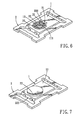
- FIG. 6 is a view similar to FIG. 5 , but illustrating a cavity of the insulating housing filled with an encapsulating material
- FIG. 7 is a perspective view of an LED package structure including one of the lead frame units of the preferred embodiment without the connecting strips, and including the insulating housing, the LED die, the conductive wires, and an optical lens, illustrating the optical lens disposed on a top surface of the insulating housing for covering the encapsulating material;
- FIG. 8 is a perspective view of the LED package structure
- FIG. 9 is a sectional view of the LED package structure.
- a preferred embodiment of a lead frame assembly 200 comprises a plurality of lead frame units 2 connected to each other.
- Each of the lead frame units 2 includes a first lead frame portion 21 , a second lead frame portion 22 , a pair of first side strips 24 , a pair of second side strips 20 , and a plurality of connecting strips 23 .
- the first side strips 24 of each of the lead frame units 2 are arranged in a first direction (X), and are aligned with and spaced apart from each other.
- the first side strips 24 of each of the lead frame units 2 extend along a second direction (Y) different from the first direction (X), and flank the first and second lead frame portions 21 , 22 of a corresponding one of the lead frame units 2 .
- the second side strips 20 of each of the lead frame units 2 are arranged in the second direction (Y), are aligned with and spaced apart from each other, and flank the first and second lead frame portions 21 , 22 of a corresponding one of the lead frame units 2 .
- Each of the second side strips 20 of each of the lead frame units 2 is connected between the first side strips 24 of a corresponding one of the lead frame units 2 .
- the connecting strips 23 of each of the lead frame units 2 connect the first lead frame portion 21 and the second lead frame portion 22 of a corresponding one of the lead frame units 2 with the first side strips 24 of the corresponding one of the lead frame units 2 .
- Any two adjacent ones of the lead frame units 2 have two interconnected first side strips 24 or two interconnected second side strips 20 that are formed with each other.
- the configurations of the lead frame units 2 are substantially the same. Therefore, only one of the lead frame units 2 will be described in the following.
- the first lead frame portion 21 of the lead frame unit 2 has a die-bonding area 211 adapted for mounting a light emitting diode (LED) die 30 (shown in FIG. 5 ).
- the second lead frame portion 22 of the lead frame unit 2 has a conductive portion 221 , a conductive surface 222 , and a bent portion 223 .
- the conductive surface 222 of the second lead frame portion 22 constitutes a top surface of the conductive portion 221 of the second lead frame portion 22 .
- the bent portion 223 is bent upwardly to connect with the conductive portion 221 such that the conductive surface 222 is disposed higher than the LED die 30 when the lead frame unit 2 is disposed on a horizontal surface such that the conductive surface 222 faces upwardly.
- an insulating housing 1 is molded on the lead frame unit 2 .
- the second side strips 20 of the lead frame unit 2 extend into the insulating housing 1 to connect to the second side strips 20 , which is advantageous for subsequent manufacturing process.
- the insulating housing 1 has a top surface 11 that is formed with a cavity 12 .
- a plastic material such as epoxy resin or silica gel, is injected onto the lead frame unit 2 to form the insulating housing 1 in an in-mold injection manner.
- the first lead frame portion 21 and the second lead frame portion 22 (see FIG. 3 ) of the lead frame unit 2 are covered by the insulating housing 1 .
- the die-bonding area 211 (see FIG. 3 ) of the first lead frame portion 21 of the lead frame unit 2 is exposed within the cavity 12 of the insulating housing 1 and is adapted for mounting the LED die 30 (see FIG. 5 ).
- the conductive surface 222 of the second lead frame portion 22 of the lead frame unit 2 and the top surface 11 of the insulating housing 1 are located in a plane. It should be noted that the conductive surface 222 of the second lead frame portion 22 may be disposed higher than the top surface 11 of the insulating housing 1 in other preferred embodiments. As such, the conductive surface 222 of the second lead frame portion 22 of the lead frame unit 2 is exposed outwardly of the top surface 11 of the insulating housing 1 and can be adapted for electrical connection with conductive wires 31 (see FIG. 5 ).
- the top surface 11 of the insulating housing 1 has a rough portion 111 surrounding the cavity 12 of the insulating housing 1 . In this preferred embodiment, the rough portion 111 is formed with a plurality of protrusions.
- the connecting strips 23 can be removed from the lead frame unit 2 .
- the conductive wires 31 are bonded to the first and second lead frame portions 21 , 22 (shown in FIG. 3 ), such that each of the conductive wires 31 has one end connected fixedly to the conductive surface 222 of the second lead frame portion 22 , and the other end extending into the cavity 12 of the insulating housing 1 and connected fixedly to an electrode contact (not shown) of the LED die 30 .
- the cavity 12 of the insulating housing 1 is rectangular and is defined by an inner surface 120 .
- the LED die 30 is rectangular, and the inner surface 120 defining the cavity 12 is substantially vertical and has a light reflection property. A distance between the LED die 30 and the inner surface 120 is smaller than 0.6 mm. Light emitted by the LED die 30 has a wavelength that is between ultraviolet and infrared ray.
- the LED package structure 300 further comprises an encapsulating material 32 (see FIG. 6 ) and an optical lens 33 (see FIG. 7 ).
- the encapsulating material 32 is filled in the cavity 12 of the insulating housing 1 , covers the LED die 30 , and includes fluorescent powders that convert light emitted by the LED die 30 so as to output uniform illumination.
- the optical lens 33 is disposed on the top surface 11 of the insulating housing 1 for covering the encapsulating material 32 and the rough portion 111 of the insulating housing 1 . Due to the presence of the rough portion 111 of the insulating housing 1 , a contact area between the insulating housing 1 and the optical lens 33 of the LED package structure 300 is increased, thus providing a firm connection between the insulating housing 1 and the optical lens 33 .
- the encapsulating material 32 and the optical lens 33 are made of the same material.
- the first and second side strips 24 , 20 of the lead frame unit 2 are removed.
- the configuration of the lead frame unit 2 is not limited to this preferred embodiment, as long as a portion of one of the first and second lead frame portions 21 , 22 is disposed higher than the LED die 30 and is exposed outwardly of the top surface 11 of the insulating housing 1 to allow the conductive wires 31 to be bonded to the conductive surface 222 and the LED die 30 .
- the advantages of the LED package structure 300 according to the present invention are as outlined in the following.
- the conductive portion 221 of the second lead frame portion 22 of the lead frame unit 2 is exposed outwardly of the insulating housing 1 . Therefore, it is convenient to bond the conductive wires 31 to the lead frame unit 2 without increasing the dimensions of the cavity 12 of the insulating housing 1 .
- the thickness of the encapsulating material 32 is decreased as compared to that of the conventional LED package structure 9 (see FIG. 1 ), such that light emitted by the LED die 30 is transmitted into the encapsulating material 32 to reach the fluorescent powders within a short time, and is converted by the fluorescent powders to output uniform illumination.
- the LED package structure 300 of the present invention is easier to fabricate and the manufacturing costs are decreased as compared to the conventional LED package structure 8 that employs a ceramic housing 81 .
Landscapes
- Led Device Packages (AREA)
Abstract
Description
Claims (15)
Applications Claiming Priority (3)
| Application Number | Priority Date | Filing Date | Title |
|---|---|---|---|
| CN200910037562 | 2009-02-26 | ||
| CN2009100375622A CN101499446B (en) | 2009-02-26 | 2009-02-26 | Wire frame tablet, packaging structure and LED packaging structure |
| CN200910037562.2 | 2009-02-26 |
Publications (2)
| Publication Number | Publication Date |
|---|---|
| US20100213484A1 US20100213484A1 (en) | 2010-08-26 |
| US8455970B2 true US8455970B2 (en) | 2013-06-04 |
Family
ID=40946434
Family Applications (1)
| Application Number | Title | Priority Date | Filing Date |
|---|---|---|---|
| US12/654,947 Active 2031-08-07 US8455970B2 (en) | 2009-02-26 | 2010-01-11 | Lead frame assembly, package structure and LED package structure |
Country Status (2)
| Country | Link |
|---|---|
| US (1) | US8455970B2 (en) |
| CN (1) | CN101499446B (en) |
Families Citing this family (10)
| Publication number | Priority date | Publication date | Assignee | Title |
|---|---|---|---|---|
| JP2013069903A (en) * | 2011-09-22 | 2013-04-18 | Fusheng Industrial Co Ltd | Light emission diode support frame construction, and manufacturing method thereof (1) |
| DE102011056700A1 (en) * | 2011-12-20 | 2013-06-20 | Osram Opto Semiconductors Gmbh | Process for the production of optoelectronic semiconductor components, lead frame composite and optoelectronic semiconductor component |
| US9299687B2 (en) | 2012-10-05 | 2016-03-29 | Bridgelux, Inc. | Light-emitting assemblies comprising an array of light-emitting diodes having an optimized lens configuration |
| JP6094804B2 (en) * | 2013-04-02 | 2017-03-15 | 東芝ライテック株式会社 | LIGHTING DEVICE AND VEHICLE LIGHT |
| TWI565100B (en) * | 2014-01-28 | 2017-01-01 | 林俊明 | An electronic component bracket with a roughened surface |
| JP6671117B2 (en) | 2014-07-08 | 2020-03-25 | エルジー イノテック カンパニー リミテッド | Light emitting device package |
| KR102252156B1 (en) | 2014-07-08 | 2021-05-17 | 엘지이노텍 주식회사 | Light emitting device package |
| KR101668353B1 (en) * | 2014-11-03 | 2016-10-21 | (주)포인트엔지니어링 | Chip Substrate and Chip Package Module |
| US11431146B2 (en) * | 2015-03-27 | 2022-08-30 | Jabil Inc. | Chip on submount module |
| KR102111635B1 (en) * | 2018-02-23 | 2020-05-26 | 주식회사 옵티맥 | laser projector |
Citations (16)
| Publication number | Priority date | Publication date | Assignee | Title |
|---|---|---|---|---|
| US3924246A (en) * | 1974-05-15 | 1975-12-02 | Isotronics Inc | Ultraviolet-transmitting window |
| US4710797A (en) * | 1983-03-14 | 1987-12-01 | Oki Electric Industry Co., Ltd. | Erasable and programable read only memory devices |
| US5068713A (en) * | 1988-08-18 | 1991-11-26 | Seiko Epson Corporation | Solid state image sensing device |
| US5291038A (en) * | 1990-12-19 | 1994-03-01 | Sharp Kabushiki Kaisha | Reflective type photointerrupter |
| US6066861A (en) | 1996-09-20 | 2000-05-23 | Siemens Aktiengesellschaft | Wavelength-converting casting composition and its use |
| US6340824B1 (en) * | 1997-09-01 | 2002-01-22 | Kabushiki Kaisha Toshiba | Semiconductor light emitting device including a fluorescent material |
| US6417019B1 (en) | 2001-04-04 | 2002-07-09 | Lumileds Lighting, U.S., Llc | Phosphor converted light emitting diode |
| US6576488B2 (en) | 2001-06-11 | 2003-06-10 | Lumileds Lighting U.S., Llc | Using electrophoresis to produce a conformally coated phosphor-converted light emitting semiconductor |
| US6621616B1 (en) * | 1998-08-21 | 2003-09-16 | Gentex Corporation | Devices incorporating electrochromic elements and optical sensors |
| US7129638B2 (en) | 2000-08-09 | 2006-10-31 | Avago Technologies General Ip (Singapore) Pte. Ltd. | Light emitting devices with a phosphor coating having evenly dispersed phosphor particles and constant thickness |
| US20070108561A1 (en) * | 2005-11-16 | 2007-05-17 | Altus Technology Inc. | Image sensor chip package |
| US7408205B2 (en) * | 2005-12-02 | 2008-08-05 | Altus Technology Inc. | Digital camera module |
| US20090173957A1 (en) * | 2005-06-23 | 2009-07-09 | Osram Opto Semiconductors Gmbh | Wavelength-converting converter material, light-emitting optical component, and method for the production thereof |
| US7695990B2 (en) * | 2002-08-05 | 2010-04-13 | Osram Opto Semiconductors Gmbh | Fabricating surface mountable semiconductor components with leadframe strips |
| US7728507B2 (en) * | 2005-09-30 | 2010-06-01 | Osram Opto Semiconductors Gmbh | Radiation-emitting component provided with metallic injected-molded carrier |
| US7838899B2 (en) * | 2006-01-04 | 2010-11-23 | Stats Chippac Ltd. | Integrated circuit package system with image sensor system |
-
2009
- 2009-02-26 CN CN2009100375622A patent/CN101499446B/en active Active
-
2010
- 2010-01-11 US US12/654,947 patent/US8455970B2/en active Active
Patent Citations (16)
| Publication number | Priority date | Publication date | Assignee | Title |
|---|---|---|---|---|
| US3924246A (en) * | 1974-05-15 | 1975-12-02 | Isotronics Inc | Ultraviolet-transmitting window |
| US4710797A (en) * | 1983-03-14 | 1987-12-01 | Oki Electric Industry Co., Ltd. | Erasable and programable read only memory devices |
| US5068713A (en) * | 1988-08-18 | 1991-11-26 | Seiko Epson Corporation | Solid state image sensing device |
| US5291038A (en) * | 1990-12-19 | 1994-03-01 | Sharp Kabushiki Kaisha | Reflective type photointerrupter |
| US6066861A (en) | 1996-09-20 | 2000-05-23 | Siemens Aktiengesellschaft | Wavelength-converting casting composition and its use |
| US6340824B1 (en) * | 1997-09-01 | 2002-01-22 | Kabushiki Kaisha Toshiba | Semiconductor light emitting device including a fluorescent material |
| US6621616B1 (en) * | 1998-08-21 | 2003-09-16 | Gentex Corporation | Devices incorporating electrochromic elements and optical sensors |
| US7129638B2 (en) | 2000-08-09 | 2006-10-31 | Avago Technologies General Ip (Singapore) Pte. Ltd. | Light emitting devices with a phosphor coating having evenly dispersed phosphor particles and constant thickness |
| US6417019B1 (en) | 2001-04-04 | 2002-07-09 | Lumileds Lighting, U.S., Llc | Phosphor converted light emitting diode |
| US6576488B2 (en) | 2001-06-11 | 2003-06-10 | Lumileds Lighting U.S., Llc | Using electrophoresis to produce a conformally coated phosphor-converted light emitting semiconductor |
| US7695990B2 (en) * | 2002-08-05 | 2010-04-13 | Osram Opto Semiconductors Gmbh | Fabricating surface mountable semiconductor components with leadframe strips |
| US20090173957A1 (en) * | 2005-06-23 | 2009-07-09 | Osram Opto Semiconductors Gmbh | Wavelength-converting converter material, light-emitting optical component, and method for the production thereof |
| US7728507B2 (en) * | 2005-09-30 | 2010-06-01 | Osram Opto Semiconductors Gmbh | Radiation-emitting component provided with metallic injected-molded carrier |
| US20070108561A1 (en) * | 2005-11-16 | 2007-05-17 | Altus Technology Inc. | Image sensor chip package |
| US7408205B2 (en) * | 2005-12-02 | 2008-08-05 | Altus Technology Inc. | Digital camera module |
| US7838899B2 (en) * | 2006-01-04 | 2010-11-23 | Stats Chippac Ltd. | Integrated circuit package system with image sensor system |
Also Published As
| Publication number | Publication date |
|---|---|
| US20100213484A1 (en) | 2010-08-26 |
| CN101499446A (en) | 2009-08-05 |
| CN101499446B (en) | 2013-10-16 |
Similar Documents
| Publication | Publication Date | Title |
|---|---|---|
| US8455970B2 (en) | Lead frame assembly, package structure and LED package structure | |
| US8482023B2 (en) | Leadframe having a heat sink supporting part, fabricating method of a light emitting diode package using the same, and light emitting diode package fabricated by the method | |
| US8735931B2 (en) | Light emitting diode package and fabrication method thereof | |
| EP2654093B1 (en) | Package and method for manufacturing package | |
| EP2218116B1 (en) | Slim led package | |
| KR100757196B1 (en) | Light emitting device having a silicon lens | |
| US8421174B2 (en) | Light emitting diode package structure | |
| US9698312B2 (en) | Resin package and light emitting device | |
| JP2010516050A (en) | Housing for optoelectronic components and placement of optoelectronic components in the housing | |
| KR100899554B1 (en) | Light emitting diode package and its manufacturing method | |
| KR20110128592A (en) | LED Package | |
| US8900895B2 (en) | Method for manufacturing LED package | |
| US20150021648A1 (en) | Composite led package and its application to light tubes | |
| JP2010153861A (en) | Light emitting diode package structure | |
| JP2016533641A (en) | Optoelectronic component and manufacturing method thereof | |
| JP2004095576A (en) | Optical semiconductor device, optical semiconductor module, and method of manufacturing optical semiconductor device | |
| KR20120083080A (en) | Light emitting device package and method of manufacturing the light emitting device package | |
| KR100995913B1 (en) | Photo interrupter and its manufacturing method | |
| KR101377603B1 (en) | Side-view light emitting device package and backlight unit comprising the same | |
| KR100877550B1 (en) | LED package using LED lead panel | |
| KR20120069072A (en) | Light emitting device | |
| US20120139002A1 (en) | Led package structure and method for manufacturing the same | |
| KR101274045B1 (en) | Light emitting diode and method for producing the same | |
| CN101271943A (en) | LED module structure and manufacturing method thereof | |
| JP2018511176A (en) | Optoelectronic component and manufacturing method thereof |
Legal Events
| Date | Code | Title | Description |
|---|---|---|---|
| AS | Assignment |
Owner name: LITE-ON TECHNOLOGY CORP., TAIWAN Free format text: ASSIGNMENT OF ASSIGNORS INTEREST;ASSIGNOR:LIN, CHEN-HSIU;REEL/FRAME:023829/0754 Effective date: 20100104 Owner name: SILITEK ELECTRONIC (GUANGZHOU) CO., LTD., CHINA Free format text: ASSIGNMENT OF ASSIGNORS INTEREST;ASSIGNOR:LIN, CHEN-HSIU;REEL/FRAME:023829/0754 Effective date: 20100104 |
|
| AS | Assignment |
Owner name: LITE-ON ELECTRONICS (GUANGZHOU) LIMITED, CHINA Free format text: CHANGE OF NAME;ASSIGNOR:SILITEK ELECTRONIC (GUANGZHOU) CO., LTD.;REEL/FRAME:030401/0501 Effective date: 20120731 |
|
| STCF | Information on status: patent grant |
Free format text: PATENTED CASE |
|
| FPAY | Fee payment |
Year of fee payment: 4 |
|
| MAFP | Maintenance fee payment |
Free format text: PAYMENT OF MAINTENANCE FEE, 8TH YEAR, LARGE ENTITY (ORIGINAL EVENT CODE: M1552); ENTITY STATUS OF PATENT OWNER: LARGE ENTITY Year of fee payment: 8 |
|
| MAFP | Maintenance fee payment |
Free format text: PAYMENT OF MAINTENANCE FEE, 12TH YEAR, LARGE ENTITY (ORIGINAL EVENT CODE: M1553); ENTITY STATUS OF PATENT OWNER: LARGE ENTITY Year of fee payment: 12 |