US8445349B2 - Method of manufacturing nonvolatile semiconductor memory device - Google Patents
Method of manufacturing nonvolatile semiconductor memory device Download PDFInfo
- Publication number
- US8445349B2 US8445349B2 US13/358,633 US201213358633A US8445349B2 US 8445349 B2 US8445349 B2 US 8445349B2 US 201213358633 A US201213358633 A US 201213358633A US 8445349 B2 US8445349 B2 US 8445349B2
- Authority
- US
- United States
- Prior art keywords
- transistors
- insulators
- memory cell
- selection
- substrate
- Prior art date
- Legal status (The legal status is an assumption and is not a legal conclusion. Google has not performed a legal analysis and makes no representation as to the accuracy of the status listed.)
- Active
Links
- 239000004065 semiconductor Substances 0.000 title claims abstract description 16
- 238000004519 manufacturing process Methods 0.000 title claims abstract description 13
- 239000012212 insulator Substances 0.000 claims abstract description 96
- 239000000758 substrate Substances 0.000 claims abstract description 66
- 238000000034 method Methods 0.000 claims abstract description 56
- 238000005530 etching Methods 0.000 claims abstract description 36
- 238000009792 diffusion process Methods 0.000 claims description 37
- 230000002093 peripheral effect Effects 0.000 claims description 37
- 239000012535 impurity Substances 0.000 claims description 33
- 150000002500 ions Chemical class 0.000 claims description 20
- 229910052581 Si3N4 Inorganic materials 0.000 claims description 12
- HQVNEWCFYHHQES-UHFFFAOYSA-N silicon nitride Chemical compound N12[Si]34N5[Si]62N3[Si]51N64 HQVNEWCFYHHQES-UHFFFAOYSA-N 0.000 claims description 12
- VYPSYNLAJGMNEJ-UHFFFAOYSA-N Silicium dioxide Chemical compound O=[Si]=O VYPSYNLAJGMNEJ-UHFFFAOYSA-N 0.000 claims description 5
- 230000015572 biosynthetic process Effects 0.000 claims description 5
- 229910052814 silicon oxide Inorganic materials 0.000 claims description 5
- 238000005755 formation reaction Methods 0.000 claims 3
- 238000002513 implantation Methods 0.000 claims 2
- 239000010410 layer Substances 0.000 description 198
- 239000011229 interlayer Substances 0.000 description 24
- 238000001039 wet etching Methods 0.000 description 13
- 238000001459 lithography Methods 0.000 description 12
- 238000005468 ion implantation Methods 0.000 description 9
- 239000003989 dielectric material Substances 0.000 description 7
- NBIIXXVUZAFLBC-UHFFFAOYSA-N Phosphoric acid Chemical compound OP(O)(O)=O NBIIXXVUZAFLBC-UHFFFAOYSA-N 0.000 description 5
- 230000000694 effects Effects 0.000 description 5
- 239000000463 material Substances 0.000 description 5
- PXHVJJICTQNCMI-UHFFFAOYSA-N nickel Substances [Ni] PXHVJJICTQNCMI-UHFFFAOYSA-N 0.000 description 5
- 238000001020 plasma etching Methods 0.000 description 5
- 239000000126 substance Substances 0.000 description 5
- ZOXJGFHDIHLPTG-UHFFFAOYSA-N Boron Chemical compound [B] ZOXJGFHDIHLPTG-UHFFFAOYSA-N 0.000 description 4
- 229910052796 boron Inorganic materials 0.000 description 4
- 229910021332 silicide Inorganic materials 0.000 description 4
- FVBUAEGBCNSCDD-UHFFFAOYSA-N silicide(4-) Chemical compound [Si-4] FVBUAEGBCNSCDD-UHFFFAOYSA-N 0.000 description 4
- 239000000243 solution Substances 0.000 description 4
- 238000007796 conventional method Methods 0.000 description 3
- 229910052751 metal Inorganic materials 0.000 description 3
- 239000002184 metal Substances 0.000 description 3
- BOTDANWDWHJENH-UHFFFAOYSA-N Tetraethyl orthosilicate Chemical compound CCO[Si](OCC)(OCC)OCC BOTDANWDWHJENH-UHFFFAOYSA-N 0.000 description 2
- 229910000147 aluminium phosphate Inorganic materials 0.000 description 2
- 239000007864 aqueous solution Substances 0.000 description 2
- 229910052785 arsenic Inorganic materials 0.000 description 2
- RQNWIZPPADIBDY-UHFFFAOYSA-N arsenic atom Chemical compound [As] RQNWIZPPADIBDY-UHFFFAOYSA-N 0.000 description 2
- 239000005388 borosilicate glass Substances 0.000 description 2
- 238000006243 chemical reaction Methods 0.000 description 2
- 238000010438 heat treatment Methods 0.000 description 2
- 230000004048 modification Effects 0.000 description 2
- 238000012986 modification Methods 0.000 description 2
- XUIMIQQOPSSXEZ-UHFFFAOYSA-N Silicon Chemical compound [Si] XUIMIQQOPSSXEZ-UHFFFAOYSA-N 0.000 description 1
- 239000002019 doping agent Substances 0.000 description 1
- 238000002955 isolation Methods 0.000 description 1
- 229910052750 molybdenum Inorganic materials 0.000 description 1
- 229910052759 nickel Inorganic materials 0.000 description 1
- 229910052763 palladium Inorganic materials 0.000 description 1
- 229910052697 platinum Inorganic materials 0.000 description 1
- 238000005498 polishing Methods 0.000 description 1
- 239000005368 silicate glass Substances 0.000 description 1
- 229910052710 silicon Inorganic materials 0.000 description 1
- 239000010703 silicon Substances 0.000 description 1
- 238000006467 substitution reaction Methods 0.000 description 1
- 229910052715 tantalum Inorganic materials 0.000 description 1
Images


Classifications
-
- H—ELECTRICITY
- H10—SEMICONDUCTOR DEVICES; ELECTRIC SOLID-STATE DEVICES NOT OTHERWISE PROVIDED FOR
- H10B—ELECTRONIC MEMORY DEVICES
- H10B41/00—Electrically erasable-and-programmable ROM [EEPROM] devices comprising floating gates
- H10B41/40—Electrically erasable-and-programmable ROM [EEPROM] devices comprising floating gates characterised by the peripheral circuit region
- H10B41/41—Electrically erasable-and-programmable ROM [EEPROM] devices comprising floating gates characterised by the peripheral circuit region of a memory region comprising a cell select transistor, e.g. NAND
-
- H—ELECTRICITY
- H01—ELECTRIC ELEMENTS
- H01L—SEMICONDUCTOR DEVICES NOT COVERED BY CLASS H10
- H01L21/00—Processes or apparatus adapted for the manufacture or treatment of semiconductor or solid state devices or of parts thereof
- H01L21/70—Manufacture or treatment of devices consisting of a plurality of solid state components formed in or on a common substrate or of parts thereof; Manufacture of integrated circuit devices or of parts thereof
- H01L21/77—Manufacture or treatment of devices consisting of a plurality of solid state components or integrated circuits formed in, or on, a common substrate
- H01L21/78—Manufacture or treatment of devices consisting of a plurality of solid state components or integrated circuits formed in, or on, a common substrate with subsequent division of the substrate into plural individual devices
- H01L21/82—Manufacture or treatment of devices consisting of a plurality of solid state components or integrated circuits formed in, or on, a common substrate with subsequent division of the substrate into plural individual devices to produce devices, e.g. integrated circuits, each consisting of a plurality of components
- H01L21/822—Manufacture or treatment of devices consisting of a plurality of solid state components or integrated circuits formed in, or on, a common substrate with subsequent division of the substrate into plural individual devices to produce devices, e.g. integrated circuits, each consisting of a plurality of components the substrate being a semiconductor, using silicon technology
- H01L21/8232—Field-effect technology
- H01L21/8234—MIS technology, i.e. integration processes of field effect transistors of the conductor-insulator-semiconductor type
- H01L21/823418—MIS technology, i.e. integration processes of field effect transistors of the conductor-insulator-semiconductor type with a particular manufacturing method of the source or drain structures, e.g. specific source or drain implants or silicided source or drain structures or raised source or drain structures
- H01L21/823425—MIS technology, i.e. integration processes of field effect transistors of the conductor-insulator-semiconductor type with a particular manufacturing method of the source or drain structures, e.g. specific source or drain implants or silicided source or drain structures or raised source or drain structures manufacturing common source or drain regions between a plurality of conductor-insulator-semiconductor structures
-
- H—ELECTRICITY
- H01—ELECTRIC ELEMENTS
- H01L—SEMICONDUCTOR DEVICES NOT COVERED BY CLASS H10
- H01L21/00—Processes or apparatus adapted for the manufacture or treatment of semiconductor or solid state devices or of parts thereof
- H01L21/70—Manufacture or treatment of devices consisting of a plurality of solid state components formed in or on a common substrate or of parts thereof; Manufacture of integrated circuit devices or of parts thereof
- H01L21/77—Manufacture or treatment of devices consisting of a plurality of solid state components or integrated circuits formed in, or on, a common substrate
- H01L21/78—Manufacture or treatment of devices consisting of a plurality of solid state components or integrated circuits formed in, or on, a common substrate with subsequent division of the substrate into plural individual devices
- H01L21/82—Manufacture or treatment of devices consisting of a plurality of solid state components or integrated circuits formed in, or on, a common substrate with subsequent division of the substrate into plural individual devices to produce devices, e.g. integrated circuits, each consisting of a plurality of components
- H01L21/822—Manufacture or treatment of devices consisting of a plurality of solid state components or integrated circuits formed in, or on, a common substrate with subsequent division of the substrate into plural individual devices to produce devices, e.g. integrated circuits, each consisting of a plurality of components the substrate being a semiconductor, using silicon technology
- H01L21/8232—Field-effect technology
- H01L21/8234—MIS technology, i.e. integration processes of field effect transistors of the conductor-insulator-semiconductor type
- H01L21/823468—MIS technology, i.e. integration processes of field effect transistors of the conductor-insulator-semiconductor type with a particular manufacturing method of the gate sidewall spacers, e.g. double spacers, particular spacer material or shape
-
- H—ELECTRICITY
- H01—ELECTRIC ELEMENTS
- H01L—SEMICONDUCTOR DEVICES NOT COVERED BY CLASS H10
- H01L29/00—Semiconductor devices adapted for rectifying, amplifying, oscillating or switching, or capacitors or resistors with at least one potential-jump barrier or surface barrier, e.g. PN junction depletion layer or carrier concentration layer; Details of semiconductor bodies or of electrodes thereof ; Multistep manufacturing processes therefor
- H01L29/66—Types of semiconductor device ; Multistep manufacturing processes therefor
- H01L29/66007—Multistep manufacturing processes
- H01L29/66075—Multistep manufacturing processes of devices having semiconductor bodies comprising group 14 or group 13/15 materials
- H01L29/66227—Multistep manufacturing processes of devices having semiconductor bodies comprising group 14 or group 13/15 materials the devices being controllable only by the electric current supplied or the electric potential applied, to an electrode which does not carry the current to be rectified, amplified or switched, e.g. three-terminal devices
- H01L29/66409—Unipolar field-effect transistors
- H01L29/66477—Unipolar field-effect transistors with an insulated gate, i.e. MISFET
- H01L29/6653—Unipolar field-effect transistors with an insulated gate, i.e. MISFET using the removal of at least part of spacer, e.g. disposable spacer
-
- H—ELECTRICITY
- H10—SEMICONDUCTOR DEVICES; ELECTRIC SOLID-STATE DEVICES NOT OTHERWISE PROVIDED FOR
- H10B—ELECTRONIC MEMORY DEVICES
- H10B41/00—Electrically erasable-and-programmable ROM [EEPROM] devices comprising floating gates
- H10B41/30—Electrically erasable-and-programmable ROM [EEPROM] devices comprising floating gates characterised by the memory core region
- H10B41/35—Electrically erasable-and-programmable ROM [EEPROM] devices comprising floating gates characterised by the memory core region with a cell select transistor, e.g. NAND
Definitions
- Embodiments described herein relate to a method of manufacturing a nonvolatile semiconductor memory device.
- a nonvolatile semiconductor memory device such as a NAND type flash memory has been increased in capacity and reduced in size year after year in accordance with the progress of micro-fabrication techniques for reducing the size of memory cells of the device. It is desired for the device to further improve the yield and reduce the cost.
- a sacrificial layer is formed between memory cell transistors, in sidewall insulators of selection transistors, and in sidewall insulators of peripheral transistors, and then the sacrificial layer is removed, for example.
- An example of the sacrificial layer includes a silicon nitride (SiN) layer.
- the sacrificial layer when removing the sacrificial layer, a part of the sacrificial layer may remain depending on the processing condition.
- the sacrificial layer remains, the characteristics of the transistors are changed.
- the sacrificial layer is made of the SiN layer, when a high voltage such as a write or read voltage is applied, electric charges may be trapped in the SiN layer and thereby the threshold voltages of the transistors are changed to make the circuit operation difficult. Therefore, it is desirable to prevent the sacrificial layer from remaining.
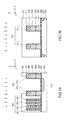
- FIGS. 1A to 5B are side cross-sectional views showing a method of manufacturing a nonvolatile semiconductor memory device of a first embodiment
- FIGS. 6A to 19B are side cross-sectional views showing a method of manufacturing a nonvolatile semiconductor memory of a second embodiment.
- An embodiment described herein is a method of manufacturing a nonvolatile semiconductor memory device, the method including forming a plurality of memory cell transistors and a plurality of selection transistors on a substrate.
- the method further includes burying first and second insulators successively between memory cell transistors and between a memory cell transistor and a selection transistor, and forming the first and second insulators successively on side surfaces of selection transistors, the side surfaces facing a space between the selection transistors.
- the method further includes burying third to fifth insulators successively between the selection transistors via the first and second insulators.
- the method further includes removing the second and fourth insulators by a first etching so that the second and fourth insulators partially remain between the selection transistors.
- the method further includes removing the second and fourth insulators remaining between the selection transistors by a second etching performed after the first etching.
- FIGS. 1A to 5B are side cross-sectional views showing a method of manufacturing a nonvolatile semiconductor memory device of a first embodiment.
- the device is a NAND type flash memory.
- the substrate 101 is a semiconductor substrate such as a silicon substrate, for example.
- FIG. 1A shows memory cell transistors MC 1 to MC 4 which configure one NAND string, as an example.
- FIG. 1A further shows a selection transistor SG 1 which configures the NAND string, and a selection transistor SG 2 adjacent to the selection transistor SG 1 .
- FIG. 1A shows X and Y directions in parallel with the main surface of the substrate 101 , and a Z direction perpendicular to the main surface of the substrate 101 .
- the X, Y and Z directions are perpendicular to each other.
- the X direction corresponds to a direction in which the NAND string is extended.
- each of the memory cell transistors MC and the selection transistors SG includes a first insulating layer (gate insulator) 102 , a first electrode layer (floating gate layer) 103 , a second insulating layer (intergate insulator) 104 , a second electrode layer (control gate layer) 105 , and a cap layer 106 which are formed in this order on the substrate 101 .
- the second electrode layer 105 in each memory cell transistor MC configures a word line (including a dummy word line) extended in the Y direction.
- the second electrode layer 105 in each selection transistor SG configures a selection line extended in the Y direction.
- the first and second electrode layers 103 and 105 in the selection transistor SG 1 are electrically connected to each other by an opening H 1 formed in the second insulating layer 104 , so as to form a gate electrode of the selection transistor SG 1 .
- an opening H 2 and a gate electrode are similarly formed in the selection transistor SG 2 .
- a sidewall insulator 111 is formed over the whole surface of the substrate 101 .
- the sidewall insulator 111 is an example of a first insulator.
- the sidewall insulator 111 is, for example, a silicon oxide (SiO 2 ) layer.
- the substrate 101 between the memory cell transistors MC, and the substrate 101 between the memory cell transistor MC and the selection transistor SG are covered with a resist layer 131 .
- impurity ions are implanted into the substrate 101 by using the resist layer 131 as a mask.
- a first diffusion layer 121 is formed in the substrate 101 between the selection transistors SG.
- the impurity used in the ion implantation include B (boron) in the case of forming a P-type diffusion layer, and As (arsenic) in the case of forming an N-type diffusion layer.
- the resist layer 131 is removed from the substrate 101 .
- a first sacrificial layer 112 is formed over the whole surface of the substrate 101 .
- the thickness of the first sacrificial layer 112 is set to a thickness at which the gap between the memory cell transistors MC and the gap between the memory cell transistor MC and the selection transistor SG are filled with the first sacrificial layer 112 .
- the first sacrificial layer 112 is an example of a second insulator.
- the first sacrificial layer 112 is, for example, a silicon nitride (SiN) layer.
- the first insulating layer 102 , the sidewall insulator 111 , and the first sacrificial layer 112 on the surface of the substrate 101 between the selection transistors SG are removed by RIE (Reactive Ion Etching).
- the sidewall insulator 111 and the first sacrificial layer 112 are processed into the shapes as shown in FIG. 2B .
- the sidewall insulator 111 and the first sacrificial layer 112 are buried in this order between the memory cell transistors MC, and between the memory cell transistor MC and the selection transistor SG, while the sidewall insulator 111 and the first sacrificial layer 112 are formed in this order on side surfaces of the selection transistors SG, facing the space between the selection transistors SG.
- an underlying insulator 113 , a second sacrificial layer 114 , and a third sacrificial layer 115 are formed in this order over the whole surface of the substrate 101 .
- the thickness of the third sacrificial layer 115 is set to a thickness at which the gap between the selection transistors SG is filled with the third sacrificial layer 115 , and the surface of the third sacrificial layer 115 is planarized by CMP (Chemical Mechanical Polishing). The planarization is continued until the second sacrificial layer 114 is exposed.
- CMP Chemical Mechanical Polishing
- the underlying insulator 113 , the second sacrificial layer 114 , and the third sacrificial layer 115 are examples of third, fourth and fifth insulators, respectively.
- the underlying insulator 113 , the second sacrificial layer 114 , and the third sacrificial layer 115 are, for example, a silicon oxide layer, a silicon nitride layer, and a BSG (Boro-Silicate Glass) layer, respectively.
- the sidewall insulator 111 , the first sacrificial layer 112 , the underlying insulator 113 , the second sacrificial layer 114 , and the third sacrificial layer 115 are processed into the shapes as shown in FIG. 3A .
- the underlying insulator 113 , the second sacrificial layer 114 , and the third sacrificial layer 115 are buried between the selection transistors SG via the sidewall insulator 111 and the first sacrificial layer 112 .
- the first and second sacrificial layers 112 and 114 which are insulators of the same kind (e.g., SiN layers), are removed by wet etching.
- the wet etching is an example of a first etching.
- An example of a chemical solution for the wet etching includes a phosphoric acid (H 3 PO 4 ) aqueous solution.
- the character P 1 shown in FIG. 3B denotes a gap formed by removing the first sacrificial layer 112 between the memory cell transistors MC.
- the character P 2 denotes a gap formed by removing the first sacrificial layer 112 between the memory cell transistor MC and the selection transistor SG.
- the characters P 3 and P 4 denote gaps formed by removing the first sacrificial layer 112 and the second sacrificial layer 114 between the selection transistors SG, respectively.
- the width of the opening of the gap P 1 is, for example, about 20 nm, and the width of the opening of the gap P 2 is, for example, about 40 nm.
- the width of the openings of the gaps P 3 and P 4 is about 10 to 15 nm.
- the width of the openings of the gaps P 3 and P 4 is set to be smaller than the width of the openings of the gaps P 1 and P 2 , in the present embodiment. For this reason, the first and second sacrificial layers 112 and 114 in the gaps P 3 and P 4 are more difficult to be removed by the wet etching as compared with the first sacrificial layer 112 in the gaps P 1 and P 2 .
- a state as shown in FIG. 3B is caused by the wet etching.
- the first sacrificial layer 112 in the gaps P 1 and P 2 are completely removed, while the first and second sacrificial layers 112 and 114 in the gaps P 3 and P 4 are partially left.
- the wet etching which completely removes the first sacrificial layer 112 in the gaps P 1 and P 2 and which partially leaves the first and second sacrificial layers 112 and 114 in the gaps P 3 and P 4 , can be realized by adjusting the etching processing time, for example.
- the gaps P 1 , P 3 and P 4 are examples of first to third gaps, respectively.
- the first and second sacrificial layers 112 and 114 left in the gaps P 3 and P 4 are positively utilized.
- impurity ions are implanted into the substrate 101 by using the sidewall insulator 111 , the first sacrificial layer 112 , the underlying insulator 113 , the second sacrificial layer 114 , and the third sacrificial layer 115 as a mask.
- a second diffusion layer 122 is formed in the substrate 101 between the memory cell transistors MC, and between the memory cell transistor MC and the selection transistor SG.
- the impurity used by the ion implantation include B (boron) at the time of forming a P-type diffusion layer, and As (arsenic) at the time of forming an N-type diffusion layer.
- the second diffusion layer 122 is not formed in the substrate 101 between the selection transistors SG since the substrate 101 between the selection transistors SG is covered with the mask.
- the first and second sacrificial layers 112 and 114 left in the gaps P 3 and P 4 , and the third sacrificial layer 115 are removed by wet etching.
- This wet etching is an example of a second etching.
- An example of a chemical solution for this wet etching includes a phosphoric acid aqueous solution. This process is performed to avoid the state in which the sacrificial layers 112 and 114 are finally left to change the characteristics of the selection transistors SG.
- a metal layer e.g., Ni (nickel) layer
- silicide reaction is generated by heat treatment to form a silicide layer 201 in the second electrode layer 105 .
- the material of the metal layer other than Ni include Ti, Co, Pt, Pd, Ta, Mo and the like.
- a first inter layer dielectric 211 is formed over the whole surface of the substrate 101 .
- the first inter layer dielectric 211 is an example of a sixth insulator.
- the first inter layer dielectric 211 is, for example, a TEOS layer.
- examples of the material and the formation conditions of the first inter layer dielectric 211 include a material having poor embedding properties and conditions causing poor embedding properties.
- air gaps 221 remain between the memory cell transistors MC, between the memory cell transistor MC and the selection transistor SG, and in the sidewall portions of the selection transistors SG.
- second and third inter layer dielectrics 212 and 213 are formed in this order on the first inter layer dielectric 211 .
- the second and third inter layer dielectrics 212 and 213 are, for example, a silicon nitride layer and a NSG (Non-doped Silicate Glass) layer, respectively.
- the surface of the third inter layer dielectric 213 is planarized by CMP. The planarization is continued until the second inter layer dielectric 212 is exposed.
- an fourth inter layer dielectric 214 is formed on the second and third inter layer dielectrics 212 and 213 .
- the fourth inter layer dielectric 214 is a TEOS layer, for example.
- interconnect layers, via plugs, inter layer dielectrics and the like are then formed by conventional methods. In this way, the nonvolatile semiconductor memory device is manufactured.
- impurity ions are implanted into the substrate 101 by using the sidewall insulator 111 , the first sacrificial layer 112 , the underlying insulator 113 , the second sacrificial layer 114 , and the third sacrificial layer 115 as a mask.
- the details of this process will be described.
- the second diffusion layer 122 is formed in the substrate 101 .
- the first diffusion layer 121 is formed in the process of FIG. 1B . Therefore, in the present embodiment, the impurity concentration profiles in the first and second diffusion layers 121 and 122 can be made different from each other regardless of whether the kind of dopant is the same or not.
- the depth at which the impurity concentration in the second diffusion layer 122 becomes a maximum is set to be different from the depth at which the impurity concentration in the first diffusion layer 121 becomes a maximum, for example.
- the peak value of the impurity concentration in the second diffusion layer 122 is set to be different from the peak value of the impurity concentration in the first diffusion layer 121 , for example.
- the first diffusion layer 121 is formed by implanting boron into the substrate 101 at 30 keV
- the second diffusion layer 122 is formed by implanting boron into the substrate 101 at 10 keV, for example.
- the impurity concentration profiles in the first and second diffusion layers 121 and 122 are made different from each other.
- impurity ions are implanted into the substrate 101 in the state where the upper surfaces of the memory cell transistors MC and the selection transistors SG are not covered with a mask. Therefore, due to this ion implantation, impurity ions are implanted not only into the substrate 101 but also into the second electrode layers 105 of the memory cell transistors MC and the selection transistors SG.
- impurity ions are also implanted into the second electrode layers 105 of peripheral transistors PT described below.
- the first and second sacrificial layers 112 and 114 which are insulators of the same kind, are removed by the first and second etchings. Specifically, in the first etching, the sacrificial layers 112 and 114 are removed so that the sacrificial layers 112 and 114 partially remain between the selection transistors SG. The sacrificial layers 112 and 114 remaining between the selection transistors SG are then removed by the second etching.
- the sacrificial layers 112 and 114 between the selection transistors SG, which layers are hard to be removed, can be surely removed. Therefore, according to the present embodiment, the sacrificial layers 112 and 114 can be prevented from being left, and hence it is possible to suppress that the characteristics of the transistors are changed by the residual sacrificial layers 112 and 114 .
- the conditions of the second etching may be different from the conditions of the first etching.
- the conditions include processing temperature, processing time, the kind of chemical solution, the concentration of chemical solution and the like.
- the sacrificial layers 112 and 114 left in the first etching are positively utilized.
- the sidewall insulator 111 , the first sacrificial layer 112 , the underlying insulator 113 , the second sacrificial layer 114 , and the third sacrificial layer 115 are used as a mask for ion implantation.
- the manufacturing cost of the nonvolatile semiconductor memory can be reduced by reducing the number of lithography processes.
- FIGS. 6A to 19B are side cross-sectional views showing a method of manufacturing a nonvolatile semiconductor memory of the second embodiment.
- FIG. 6A , FIG. 7A , . . . and FIG. 19A show a plurality of memory cell transistors MC and a plurality of selection transistors SG arranged in the memory cell array part on the substrate 101 .
- FIG. 6B , FIG. 7B , . . . and FIG. 19B show a plurality of peripheral transistors PT arranged in a peripheral circuit part on the substrate 101 .
- the peripheral circuit part is arranged adjacent to the memory cell array part on the substrate 101 .
- Examples of the peripheral transistors PT include LV (low voltage) transistors and HV (high voltage) transistors.
- FIG. 6A , FIG. 7A , . . . and FIG. 19A is performed similarly to that shown in FIG. 1A , FIG. 1B , . . . and FIG. 5B . Further, each processing shown in FIG. 6B , FIG. 7B , . . . and FIG. 19B is performed in parallel with that shown in FIG. 6A , FIG. 7A , . . . and FIG. 19A .
- the plurality of memory cell transistors MC, the plurality of selection transistors SG, and the plurality of peripheral transistors PT are formed on the substrate 101 .
- FIG. 6B shows peripheral transistors PT 1 and PT 2 which are arranged adjacent to each other.
- the first and second electrode layers 103 and 105 of the peripheral transistor PT 1 are electrically connected to each other by an opening H 3 formed in the second insulating layer 104 so as to form a gate electrode of the peripheral transistor PT 1 .
- a gate electrode and an opening H 4 of the peripheral transistor PT 2 are similarly formed.
- the numeral 301 denotes isolation insulators 301 formed in the substrate 101 .
- the sidewall insulator 111 is formed over the whole surface of the substrate 101 .
- the side surfaces of the memory cell transistor MC, the selection transistor SG, and the peripheral transistor PT are covered with the sidewall insulator 111 .
- the spaces between the memory cell transistors MC, between the memory cell transistor MC and the selection transistor SG, and on the substrate 101 in the peripheral circuit part are covered with the resist layer 131 .
- impurity ions are implanted into the substrate 101 by using the resist film 131 as a mask.
- the first diffusion layer 121 is formed in the substrate 101 between the selection transistors SG.
- the substrate 101 in the memory cell portion is covered with a resist layer 132 .
- ion implantation into the substrate 101 is performed by using the resist layer 132 as a mask.
- a third diffusion layer 123 is formed in the substrate 101 between the peripheral transistors PT.
- the resist layer 132 is removed from the substrate 101 .
- the first sacrificial layer 112 is formed over the whole surface of the substrate 101 .
- the first insulating layer 102 , the sidewall insulator 111 , and the first sacrificial layer 112 which are formed on the surfaces of the substrate 101 between the selection transistors SG and between peripheral transistors PT are removed by RIE.
- the sidewall insulator 111 and the first sacrificial layer 112 are processed into shapes as shown in FIGS. 10A and 10B .
- the sidewall insulator 111 and the first sacrificial layer 112 are formed in this order on the side surfaces of the peripheral transistors PT, facing the space between the peripheral transistors PT.
- the underlying insulator 113 , the second sacrificial layer 114 , and the third sacrificial layer 115 are formed in this order over the whole surface of the substrate 101 . Then, the surface of the third sacrificial layer 115 is planarized by CMP. The planarization is continued until the second sacrificial layer 114 is exposed.
- FIGS. 12A and 12B RIE processing is performed until the upper surface of the second electrode layer 105 is exposed.
- the sidewall insulator 111 , the first sacrificial layer 112 , the underlying insulator 113 , the second sacrificial layer 114 , and the third sacrificial layer 115 are processed into the shapes as shown in FIGS. 12A and 12B .
- the underlying insulator 113 , the second sacrificial layer 114 , and the third sacrificial layer 115 are buried in the space between the peripheral transistors PT via the sidewall insulator 111 and the first sacrificial layer 112 .
- the first and second sacrificial layers 112 and 114 which are the same kind of insulators (e.g., SiN layers), are removed by wet etching.
- the character P 1 shown in FIG. 13A denotes a gap formed by removing the first sacrificial layer 112 between the memory cell transistors MC. Further, the character P 2 shown in FIG. 13A denotes a gap formed by removing the first sacrificial layer 112 between the memory cell transistor MC and the selection transistor SG.
- characters P 3 and P 4 shown in FIG. 13A denote gaps formed by removing the first sacrificial layer 112 and the second sacrificial layer 114 between the selection transistors SG, respectively.
- characters P 5 and P 6 shown in FIG. 13B denote gaps formed by removing the first sacrificial layer 112 and the second sacrificial layer 114 between the peripheral transistors PT, respectively.
- the width of the opening of the gap P 1 is about 20 nm, and the width of the opening of gap P 2 is about 40 nm, for example. Further, the width of the openings of the gaps P 3 to P 6 is about 10 to 15 nm, for example.
- the width of the openings of the gaps P 3 to P 6 is set to be smaller than the width of the openings of the gap P 1 and the gap P 2 .
- the first and second sacrificial layers 112 and 114 in the gaps P 3 to P 6 are more difficult to be removed by the wet etching than the first sacrificial layer 112 in the gaps P 1 and P 2 .
- the state as shown in FIGS. 13A and 13B is generated by the wet etching.
- the first sacrificial layer 112 in the gaps P 1 and P 2 is completely removed, while the first and second sacrificial layers 112 and 114 in the gaps P 3 to P 6 are partially left.
- the gaps P 1 , P 3 , P 4 , P 5 and P 6 are examples of first to fifth gaps, respectively.
- the first and second sacrificial layers 112 and 114 left in the gaps P 3 to P 6 are positively utilized.
- impurity ions are implanted into the substrate 101 by using the sidewall insulator 111 , the first sacrificial layer 112 , the underlying insulator 113 , the second sacrificial layer 114 , and the third sacrificial layer 115 as a mask.
- the second diffusion layer 122 is formed in the substrate 101 between the memory cell transistors MC and between the memory cell transistor MC and the selection transistor SG.
- the substrate 101 between the selection transistors SG and between the peripheral transistors PT is covered with the mask, and hence the second diffusion layer 122 is not formed in the substrate 101 between the selection transistors SG and between the peripheral transistors PT.
- the first and second sacrificial layers 112 and 114 which are left in the gaps P 3 to P 6 , and the third sacrificial layer 115 are removed by wet etching. This process is performed to avoid the state in which the sacrificial layers 112 and 114 are finally left to change the characteristics of the selection transistors SG.
- the silicide layer 201 is formed in the second electrode layer 105 in such a manner that a metal layer (e.g., Ni layer) is deposited over the whole surface of the substrate 101 and that a silicide reaction is then generated by heat treatment.
- a metal layer e.g., Ni layer
- the first inter layer dielectric 211 is formed over the whole surface of the substrate 101 .
- examples of the material and the formation conditions of the first inter layer dielectric 211 include a material having poor embedding properties and conditions causing poor embedding properties are adopted.
- the air gaps 221 remain between the memory cell transistors MC, between the memory cell transistor MC and the selection transistor SG, and in the sidewall portions of the selection transistors SG and the peripheral transistors PT.
- the second and third inter layer dielectrics 212 and 213 are formed in this order on the first inter layer dielectric 211 . Then, the surface of the third inter layer dielectric 213 is planarized by CMP. The planarization is continued until the second inter layer dielectric 212 is exposed.
- the fourth inter layer dielectric 214 is formed on the second and third inter layer dielectrics 212 and 213 .
- interconnect layers, via plugs, inter layer dielectrics and the like are formed by conventional methods. In this way, the nonvolatile semiconductor memory is manufactured.
- the first and second sacrificial layers 112 and 114 which are insulators of the same kind, are removed by the first and second etchings similarly to the first embodiment. Specifically, in the first etching, the sacrificial layers 112 and 114 are removed so that the sacrificial layers 112 and 114 partially remain between the selection transistors SG and between the peripheral transistors PT. Then, in the second etching, the sacrificial layers 112 and 114 remaining between the selection transistors SG and between the peripheral transistors PT are removed.
- the sacrificial layers 112 and 114 between the selection transistors SG and between the peripheral transistors PT, which are difficult to be removed, can be surely removed similarly to the first embodiment. Therefore, according to the present embodiment, the sacrificial layers 112 and 114 are prevented from being left, and hence it is possible to suppress that the characteristics of the transistors are changed by the residual sacrificial layers 112 and 114 .
- the sacrificial layers 112 and 114 left in the first etching are positively utilized.
- the sidewall insulator 111 , the first sacrificial layer 112 , the underlying insulator 113 , the second sacrificial layer 114 , and the third sacrificial layer 115 are used as a mask for ion implantation.
- the number of lithography processes is reduced, and hence it is possible to reduce the manufacturing cost of the nonvolatile semiconductor memory device.
- FIGS. 7A and 7B the effect of reducing the number of lithography processes will be described in conjunction with the description of the processes shown in FIGS. 7A and 7B , FIGS. 8A and 8B , and FIGS. 14A and 14B .
- the first and third diffusion layers 121 and 123 are respectively formed by the ion implantation using the resist films 131 and 132 as masks ( FIGS. 7A and 7B , and FIGS. 8A and 8B ). Therefore, when forming the first and second diffusion layers 121 and 123 , lithography processes are performed.
- the second diffusion layer 122 is formed by the ion implantation using the sidewall insulator 111 , the residual first sacrificial layer 112 , the underlying insulator 113 , the residual second sacrificial layer 114 , and the third sacrificial layer 115 as a mask ( FIGS. 14A and 14B ). Therefore, when forming the second diffusion layer 122 , no lithography process is necessary.
- the first to third diffusion layers 121 to 123 can be formed by two lithography processes.
- the conventional method at least three lithography processes need to be performed to form these diffusion layers.
- the first lithography process is performed to form the diffusion layer of the selection transistors SG
- the second lithography process is performed to form the diffusion layer of the peripheral transistors PT
- the third lithography process is performed to form the diffusion layer of the memory cell transistors MC.
- such diffusion layers can be formed by two lithography processes. Therefore, according to the present embodiment, the number of lithography processes is reduced, and hence it is possible to reduce the manufacturing cost of the nonvolatile semiconductor memory device.
Landscapes
- Engineering & Computer Science (AREA)
- Microelectronics & Electronic Packaging (AREA)
- Power Engineering (AREA)
- Manufacturing & Machinery (AREA)
- Physics & Mathematics (AREA)
- Condensed Matter Physics & Semiconductors (AREA)
- General Physics & Mathematics (AREA)
- Computer Hardware Design (AREA)
- Ceramic Engineering (AREA)
- Non-Volatile Memory (AREA)
- Semiconductor Memories (AREA)
Abstract
Description
Claims (20)
Applications Claiming Priority (2)
| Application Number | Priority Date | Filing Date | Title |
|---|---|---|---|
| JP2011158012A JP2013026331A (en) | 2011-07-19 | 2011-07-19 | Manufacturing method of nonvolatile semiconductor memory device |
| JP2011-158012 | 2011-07-19 |
Publications (2)
| Publication Number | Publication Date |
|---|---|
| US20130023099A1 US20130023099A1 (en) | 2013-01-24 |
| US8445349B2 true US8445349B2 (en) | 2013-05-21 |
Family
ID=47556054
Family Applications (1)
| Application Number | Title | Priority Date | Filing Date |
|---|---|---|---|
| US13/358,633 Active US8445349B2 (en) | 2011-07-19 | 2012-01-26 | Method of manufacturing nonvolatile semiconductor memory device |
Country Status (2)
| Country | Link |
|---|---|
| US (1) | US8445349B2 (en) |
| JP (1) | JP2013026331A (en) |
Cited By (1)
| Publication number | Priority date | Publication date | Assignee | Title |
|---|---|---|---|---|
| US10204825B2 (en) | 2016-12-02 | 2019-02-12 | Samsung Electronics Co., Ltd. | Semiconductor device having air gap spacers and method for fabricating the same |
Families Citing this family (1)
| Publication number | Priority date | Publication date | Assignee | Title |
|---|---|---|---|---|
| US9245898B2 (en) * | 2014-06-30 | 2016-01-26 | Sandisk Technologies Inc. | NAND flash memory integrated circuits and processes with controlled gate height |
Citations (5)
| Publication number | Priority date | Publication date | Assignee | Title |
|---|---|---|---|---|
| JP2009194305A (en) | 2008-02-18 | 2009-08-27 | Toshiba Corp | Semiconductor memory device and method for manufacturing the same |
| US20100221880A1 (en) * | 2001-01-31 | 2010-09-02 | Toshitake Yaegashi | Non-volatile semiconductor memory device and method of manufacturing the same |
| US20100237398A1 (en) * | 2009-03-23 | 2010-09-23 | Kabushiki Kaisha Toshiba | Semiconductor storage device and method for manufacturing the same |
| US20110248329A1 (en) * | 2004-08-23 | 2011-10-13 | Toshitake Yaegashi | Method of manufacturing a non-volatile nand memory semiconductor integrated circuit |
| US20120126302A1 (en) * | 2010-11-18 | 2012-05-24 | Mitsuhiko Noda | Nonvolatile semiconductor memory device and manufacturing method of the same |
-
2011
- 2011-07-19 JP JP2011158012A patent/JP2013026331A/en not_active Withdrawn
-
2012
- 2012-01-26 US US13/358,633 patent/US8445349B2/en active Active
Patent Citations (5)
| Publication number | Priority date | Publication date | Assignee | Title |
|---|---|---|---|---|
| US20100221880A1 (en) * | 2001-01-31 | 2010-09-02 | Toshitake Yaegashi | Non-volatile semiconductor memory device and method of manufacturing the same |
| US20110248329A1 (en) * | 2004-08-23 | 2011-10-13 | Toshitake Yaegashi | Method of manufacturing a non-volatile nand memory semiconductor integrated circuit |
| JP2009194305A (en) | 2008-02-18 | 2009-08-27 | Toshiba Corp | Semiconductor memory device and method for manufacturing the same |
| US20100237398A1 (en) * | 2009-03-23 | 2010-09-23 | Kabushiki Kaisha Toshiba | Semiconductor storage device and method for manufacturing the same |
| US20120126302A1 (en) * | 2010-11-18 | 2012-05-24 | Mitsuhiko Noda | Nonvolatile semiconductor memory device and manufacturing method of the same |
Cited By (1)
| Publication number | Priority date | Publication date | Assignee | Title |
|---|---|---|---|---|
| US10204825B2 (en) | 2016-12-02 | 2019-02-12 | Samsung Electronics Co., Ltd. | Semiconductor device having air gap spacers and method for fabricating the same |
Also Published As
| Publication number | Publication date |
|---|---|
| US20130023099A1 (en) | 2013-01-24 |
| JP2013026331A (en) | 2013-02-04 |
Similar Documents
| Publication | Publication Date | Title |
|---|---|---|
| JP6407488B1 (en) | Non-volatile split-gate memory cell with integrated high-K metal gate and method of making the same | |
| TWI613796B (en) | Method of forming memory array and logic devices | |
| US20120280300A1 (en) | Semiconductor device and method of manufacturing the same | |
| US8778760B2 (en) | Method of manufacturing flash memory cell | |
| JP5091452B2 (en) | Manufacturing method of semiconductor device | |
| JP2014179361A (en) | Nonvolatile semiconductor memory device, and method of manufacturing the same | |
| US8952439B2 (en) | Nonvolatile semiconductor storage device and method of manufacture thereof | |
| US20090283813A1 (en) | Nonvolatile semiconductor memory device and method for fabricating nonvolatile semiconductor memory device | |
| US20120238099A1 (en) | Method of manufacturing electronic part | |
| JP2008091614A (en) | Semiconductor device and manufacturing method thereof | |
| JP2013197482A (en) | Nonvolatile semiconductor storage device manufacturing method and nonvolatile semiconductor storage device | |
| KR100812089B1 (en) | Method of manufacturing flash memory device | |
| US8278717B2 (en) | Semiconductor memory device and method of manufacturing the same | |
| JP2009289813A (en) | Production method of non-volatile semiconductor memory device | |
| EP3497723B1 (en) | Method of forming low height split gate memory cells | |
| US8445349B2 (en) | Method of manufacturing nonvolatile semiconductor memory device | |
| US20230247830A1 (en) | Semiconductor device including nonvolatile memory device and logic device and manufacturing method of semiconductor device including nonvolatile memory device and logic device | |
| KR100951981B1 (en) | Semiconductor device and method for manufacturing the same | |
| JP2014187132A (en) | Semiconductor device | |
| JP2008177223A (en) | Semiconductor device and manufacturing method thereof | |
| JP2003023117A (en) | Method for manufacturing semiconductor integrated circuit device | |
| JP2013143482A (en) | Semiconductor device and semiconductor device manufacturing method | |
| JP2012129453A (en) | Semiconductor device and method of manufacturing semiconductor device | |
| US7838406B2 (en) | SONOS-NAND device having a storage region separated between cells | |
| JP2013065776A (en) | Semiconductor device and manufacturing method of semiconductor device |
Legal Events
| Date | Code | Title | Description |
|---|---|---|---|
| AS | Assignment |
Owner name: KABUSHIKI KAISHA TOSHIBA, JAPAN Free format text: ASSIGNMENT OF ASSIGNORS INTEREST;ASSIGNOR:NODA, MITSUHIKO;REEL/FRAME:027598/0622 Effective date: 20120116 |
|
| STCF | Information on status: patent grant |
Free format text: PATENTED CASE |
|
| CC | Certificate of correction | ||
| FEPP | Fee payment procedure |
Free format text: PAYOR NUMBER ASSIGNED (ORIGINAL EVENT CODE: ASPN); ENTITY STATUS OF PATENT OWNER: LARGE ENTITY |
|
| FPAY | Fee payment |
Year of fee payment: 4 |
|
| AS | Assignment |
Owner name: TOSHIBA MEMORY CORPORATION, JAPAN Free format text: ASSIGNMENT OF ASSIGNORS INTEREST;ASSIGNOR:KABUSHIKI KAISHA TOSHIBA;REEL/FRAME:043709/0035 Effective date: 20170706 |
|
| MAFP | Maintenance fee payment |
Free format text: PAYMENT OF MAINTENANCE FEE, 8TH YEAR, LARGE ENTITY (ORIGINAL EVENT CODE: M1552); ENTITY STATUS OF PATENT OWNER: LARGE ENTITY Year of fee payment: 8 |
|
| AS | Assignment |
Owner name: K.K. PANGEA, JAPAN Free format text: MERGER;ASSIGNOR:TOSHIBA MEMORY CORPORATION;REEL/FRAME:055659/0471 Effective date: 20180801 Owner name: TOSHIBA MEMORY CORPORATION, JAPAN Free format text: CHANGE OF NAME AND ADDRESS;ASSIGNOR:K.K. PANGEA;REEL/FRAME:055669/0401 Effective date: 20180801 Owner name: KIOXIA CORPORATION, JAPAN Free format text: CHANGE OF NAME AND ADDRESS;ASSIGNOR:TOSHIBA MEMORY CORPORATION;REEL/FRAME:055669/0001 Effective date: 20191001 |