US8441288B2 - Differential current signal circuit - Google Patents
Differential current signal circuit Download PDFInfo
- Publication number
- US8441288B2 US8441288B2 US13/089,859 US201113089859A US8441288B2 US 8441288 B2 US8441288 B2 US 8441288B2 US 201113089859 A US201113089859 A US 201113089859A US 8441288 B2 US8441288 B2 US 8441288B2
- Authority
- US
- United States
- Prior art keywords
- voltage
- current
- signal
- circuit
- load
- Prior art date
- Legal status (The legal status is an assumption and is not a legal conclusion. Google has not performed a legal analysis and makes no representation as to the accuracy of the status listed.)
- Active, expires
Links
Images
Classifications
-
- H—ELECTRICITY
- H03—ELECTRONIC CIRCUITRY
- H03F—AMPLIFIERS
- H03F1/00—Details of amplifiers with only discharge tubes, only semiconductor devices or only unspecified devices as amplifying elements
- H03F1/30—Modifications of amplifiers to reduce influence of variations of temperature or supply voltage or other physical parameters
- H03F1/301—Modifications of amplifiers to reduce influence of variations of temperature or supply voltage or other physical parameters in MOSFET amplifiers
-
- G—PHYSICS
- G05—CONTROLLING; REGULATING
- G05F—SYSTEMS FOR REGULATING ELECTRIC OR MAGNETIC VARIABLES
- G05F5/00—Systems for regulating electric variables by detecting deviations in the electric input to the system and thereby controlling a device within the system to obtain a regulated output
-
- H—ELECTRICITY
- H03—ELECTRONIC CIRCUITRY
- H03F—AMPLIFIERS
- H03F3/00—Amplifiers with only discharge tubes or only semiconductor devices as amplifying elements
- H03F3/45—Differential amplifiers
- H03F3/45071—Differential amplifiers with semiconductor devices only
- H03F3/45076—Differential amplifiers with semiconductor devices only characterised by the way of implementation of the active amplifying circuit in the differential amplifier
- H03F3/45179—Differential amplifiers with semiconductor devices only characterised by the way of implementation of the active amplifying circuit in the differential amplifier using MOSFET transistors as the active amplifying circuit
- H03F3/45183—Long tailed pairs
-
- H—ELECTRICITY
- H03—ELECTRONIC CIRCUITRY
- H03F—AMPLIFIERS
- H03F2200/00—Indexing scheme relating to amplifiers
- H03F2200/453—Controlling being realised by adding a replica circuit or by using one among multiple identical circuits as a replica circuit
-
- H—ELECTRICITY
- H03—ELECTRONIC CIRCUITRY
- H03F—AMPLIFIERS
- H03F2203/00—Indexing scheme relating to amplifiers with only discharge tubes or only semiconductor devices as amplifying elements covered by H03F3/00
- H03F2203/45—Indexing scheme relating to differential amplifiers
- H03F2203/45654—Indexing scheme relating to differential amplifiers the LC comprising one or more extra diodes not belonging to mirrors
Definitions
- This invention relates generally to electronic circuits and in particular to a circuit which provides a differential pair of current signals.
- a current signal where the level of current is adjustable throughout a range of current levels.
- a differential pair of current output signals is desirable. Using a differential pair of signals provides a circuit with greater dynamic range and noise immunity. It is also desirable in some situations to have a current output signal which is linearly proportional to an input voltage signal throughout a voltage range. This allows the output current level to be accurately adjusted over time by adjusting the input voltage range.
- a resistor circuit can be used to create a current signal that is linearly proportional to a voltage, but this does not fulfill the need for a differential pair of current output signals that are linearly proportional to an input voltage.
- a pair of source-coupled transistors can be used to create a differential pair of current output signals, but the differential pair of current output signals have a relatively small voltage operating range over which they are linearly related to the input voltage.
- the differential pair of current output signals with a circuit that provides a repeatable and stable level of output current regardless of process or temperature variations.
- the voltage operating range is offset from its desired values due to process and temperature variations.
- the variation in the resistance value of a resistor due to process or temperature variations can cause variations in the amplitude of output signals.
- Voltage offset and/or variations in signal output can cause the system that the electronic circuit is a part of to become unstable or to change states or levels undesirably.
- the disclosed invention relates to electronic circuits and in particular to a circuit which generates a differential pair of current signals, also referred to as a differential pair of current output signals.
- the electronic circuit according to the invention converts a voltage input signal into a differential pair of current output signals, where the differential pair of current output signals are linearly proportional to the voltage input signal over a voltage operating range that covers a wide range of input voltages, and where the differential pair of current output signals have reduced susceptibility to process and temperature variations.
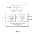
- An electronic circuit which includes a voltage to single-ended current converter circuit, where the voltage to single-ended current converter circuit outputs a single-ended current signal in response to receiving a voltage input signal, and where the single-ended current signal is linearly proportional to the voltage input signal.
- the electronic circuit according to the invention also includes a single-ended current to differential current converter circuit, where the single-ended current to differential current converter circuit outputs a differential pair of current output signals in response to receiving the single-ended current signal.
- the differential pair of current output signals are linearly proportional to the voltage input signal within a voltage operating range from a minimum operating voltage to a maximum operating voltage.
- the voltage to single-ended current converter circuit includes a voltage to linear current feedback loop circuit, where the voltage to linear current feedback loop circuit generates an interim current signal in response to receiving the voltage input signal, and where the interim current signal is linearly proportional to the voltage input signal, and where the voltage to linear current feedback loop circuit generates a current replication voltage in response to receiving the voltage input signal.
- the voltage to single-ended current converter circuit includes a current replication transistor, wherein the current replication transistor generates a single-ended current signal in response to receiving the current replication voltage, wherein the single-ended current signal is linearly proportional to the voltage input signal.
- the electronic circuit according to the invention includes a correction circuit, where the correction circuit outputs a set minimum operating voltage signal in response to receiving a correction input voltage, and where the minimum operating voltage is adjusted in response to adjusting the set minimum operating voltage signal.
- the single-ended current to differential current converter circuit includes a load mirror circuit, where the load mirror circuit outputs a load-mirrored voltage signal in response to receiving the single-ended current signal.
- the single-ended current to differential current converter circuit according to the invention includes a voltage to differential current converter circuit, where the voltage to differential current converter circuit outputs the differential pair of current output signal in response to receiving the load-mirrored voltage signal.
- the differential pair of current output signals are linearly proportional to the single-ended current signal over the voltage operating range in response to an impedance of the load mirror transistor being linearly proportional to an impedance of a load receiving a first end of the differential pair of current output signals.
- the voltage to differential current converter circuit includes a second feedback amplifier, where the second feedback amplifier outputs a second feedback amplifier output signal in response to receiving the load-mirrored voltage signal, and a source-coupled amplifier circuit which outputs the differential pair of current output signals in response to receiving the second feedback amplifier output signal.
- An electronic circuit which includes a correction circuit, where the correction circuit outputs a tracking bias signal in response to receiving a correction input voltage.
- the electronic circuit according to the invention also includes a voltage to differential current converter circuit with a converter resistor, where the voltage to differential current converter circuit outputs a first end and a second end of a differential pair of current output signals in response to receiving a voltage input signal, and where the first and the second end of the differential pair of current output signals are linearly proportional to the voltage input signal within a voltage operating range from a minimum operating voltage to a maximum operating voltage, where voltage offsets in the voltage operating range are eliminated in response to the voltage to differential current converter circuit receiving the tracking bias signal.
- the correction circuit further comprises a tracking bias resistor, where the amplitude of the tracking bias signal is a function of the resistance value of the tracking bias resistor. In some embodiments the correction circuit further comprises a set minimum operating voltage transistor, where the set minimum operating voltage transistor outputs a set minimum operating voltage signal in response to receiving the tracking bias signal. In some embodiments the minimum operating voltage of the voltage to differential current converter circuit is adjusted in response to adjustments to the set minimum operating voltage signal.
- An electronic circuit which includes a correction circuit, where the correction circuit outputs a set minimum operating voltage signal in response to receiving a correction input voltage.
- the electronic circuit also includes a voltage to differential current converter circuit, where the voltage to differential current converter circuit outputs a first end and a second end of a differential pair of current output signals in response to receiving a voltage input signal, and where the first and the second end of the differential pair of current output signals are linearly proportional to the voltage input signal throughout a voltage range from a minimum operating voltage to a maximum operating voltage.
- the minimum operating voltage is adjusted in response to adjustments to the set minimum operating voltage signal.
- the voltage to differential current converter circuit comprises a converter resistor, and variations in the minimum operating voltage of the voltage to differential current converter circuit due to variations in the resistance value of the converter resistor are eliminated in response to a first end of the converter resistor receiving the set minimum operating voltage signal.
- a method of generating a differential pair of current signals includes the step of providing a single-ended current signal to a load mirror circuit, where the load mirror circuit outputs a load-mirrored voltage signal in response to receiving the single-ended current signal, and where the load-mirrored voltage signal is a nonlinear function of the single-ended current signal.
- the method also includes the step of generating a differential pair of current signals from the load-mirrored voltage signal, where a first end of the differential pair of current signals is linearly proportional to the single-ended current signal within an operating range from a minimum current level to a maximum current level.
- the first end of the differential pair of current signals is linearly proportional to the single-ended current signal within an operating range from a minimum current level to a maximum current level in response to an impedance of the load mirror circuit being linearly proportional to an impedance of a load circuit as seen by the first end of the differential pair of current signals.
- the method also includes the step of providing the first end of the differential pair of current signals to a first load transistor.
- the method of generating a differential pair of current signal according to the invention also includes the step of providing a second end of the differential pair of current signals to a second load transistor, where the first load transistor, the second load transistor, and the load mirror circuit have the same impedance.
- the method includes the step of generating a single-ended current signal with a voltage to single-ended current converter circuit, where the voltage to single-ended current converter circuit generates the single-ended current signal in response to receiving a voltage input signal, and where the single-ended current signal is linearly proportional to the voltage input signal within a voltage operating range from a minimum operating voltage to a maximum operating voltage.
- the method also comprises the step of generating a tracking bias signal with a correction circuit, where voltage offsets in the voltage operating range are eliminated in response to the voltage to single-ended current converter circuit receiving the tracking bias signal.
- the correction circuit further comprises a tracking bias resistor, where the amplitude of the tracking bias signal is a function of the resistance value of the tracking bias resistor.
- the correction circuit outputs a set minimum operating voltage signal, where the minimum operating voltage of the voltage to single-ended current converter circuit is adjusted in response to adjustments to the set minimum operating voltage signal.
- a method of generating a differential pair of current signals includes the steps of generating a first single-ended current signal that is linearly proportional to a voltage input signal using a first feedback loop, and duplicating the first single-ended current signal to create a second single-ended current signal.
- the method according to the invention also includes the step of generating a load-mirrored voltage signal from the second single-ended current signal using a load mirror circuit, wherein the load-mirrored voltage signal is nonlinearly proportional to the second single-ended current signal.
- the method of generating a differential pair of current output signals also includes the step of generating a first end of a differential pair of current signals from the load-mirrored voltage signal using a second feedback loop, where the first end of the differential pair of current signals is linearly proportional to the voltage input signal within a voltage operating range from a minimum operating voltage to a maximum operating voltage.
- the impedance of the load mirror circuit is the same as the impedance of a first load transistor, and the first load transistor receives the first end of the differential pair of current signals.
- the method also includes the step of generating a second end of the differential pair of current signals, where the second end of the differential pair of current signals has a phase that is shifted 180 degrees with respect to a phase of the first end of the differential pair of current signals.
- the method includes the step of generating a set minimum operating voltage signal, wherein the minimum operating voltage is adjusted in response to adjusting the set minimum operating voltage signal.
- the first feedback loop includes a converter resistor, and variations in the minimum operating voltage due to variations in the resistance value of the converter resistor are neutralized in response to the first feedback loop circuit receiving the set minimum operating voltage signal.
- An electronic circuit according to the invention which includes a load mirror circuit, where the load mirror circuit converts a single-ended current signal into a load-mirrored voltage signal according to a current-to-voltage transfer function.
- the electronic circuit according to the invention also includes a voltage to differential current converter circuit, wherein the voltage to differential current converter circuit converts the load-mirrored voltage signal to a first end of a differential pair of current output signals according to a voltage-to-current transfer function, wherein the voltage-to-current transfer function is inversely proportional to the current-to-voltage transfer function.
- the current-to-voltage transfer function is nonlinear.
- the first end of the differential pair of current signals is linearly proportional to the single-ended current signal.
- the voltage to differential current converter circuit converts the load-mirrored voltage signal into a second end of the differential pair of current signals, wherein the second end of the differential pair of current signals has a phase that is shifted 180 degrees from a phase of the first end of the differential pair of current signals.
- the electronic circuit according to the invention also includes a voltage to single-ended current converter circuit.
- the voltage to single-ended current converter circuit includes a voltage to linear current feedback loop circuit and a current replication transistor.
- the voltage to linear current feedback loop circuit generates an interim current signal in response to receiving a voltage input signal, where the interim current signal is linearly proportional to the voltage input signal.
- the voltage to linear current feedback loop circuit also generates a current replication voltage in response to receiving the voltage input signal.
- the voltage to single-ended current converter circuit according to the invention also includes a current replication transistor.
- the current replication transistor generates the single-ended current signal in response to receiving the current replication voltage, where the single-ended current signal is linearly proportional to the voltage input signal.
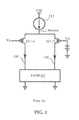
- FIG. 1 is a schematic embodiment of a source-coupled amplifier circuit as is known in the art.
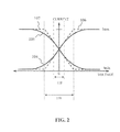
- FIG. 2 shows the voltage-to-current transfer function of the source-coupled amplifier circuit of FIG. 1 , indicated by solid lines 104 and 105 , and a desired voltage-to-current transfer function indicated by dotted lines 106 and 107 .
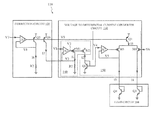
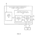
- FIG. 3 shows a block diagram of differential current signal circuit 110 according to the invention.
- FIG. 4 is a schematic diagram of one embodiment of differential current signal circuit 110 of FIG. 3 .
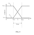
- FIG. 5 is the voltage-to-current transfer function of differential current signal circuit 110 of FIG. 3 and FIG. 4 .
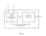
- FIG. 6 is a block diagram of voltage to single-ended current converter circuit 140 according to the invention of differential current signal circuit 110 of FIG. 3 .
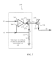
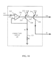
- FIG. 7 is a schematic diagram of one embodiment of voltage to single-ended current converter circuit 140 of FIG. 6
- FIG. 8 is a block diagram of single-ended current to differential current converter circuit 150 according to the invention of differential current signal circuit 110 of FIG. 3 , and load circuit 168 .
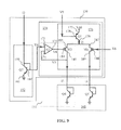
- FIG. 9 is a schematic diagram of one embodiment of single-ended current to differential current converter circuit 150 and load circuit 168 of FIG. 8 .
- FIG. 10 is a schematic diagram of one embodiment of correction circuit 120 of FIG. 3 .
- FIG. 11 illustrates method 300 of generating a differential pair of current output signals according to the invention.
- FIG. 12 illustrates method 400 of generating a differential pair of current output signals according to the invention.
- embodiments of the present invention relate to electronic circuits and in particular to an electronic circuit which provides a differential pair of current output signals.
- the electronic circuit according to the invention converts a voltage input signal into a differential pair of current output signals, where the differential pair of current output signals are linearly proportional to the voltage input signal over a voltage operating range that covers a wide range of input voltages, and where the differential pair of current output signals have reduced susceptibility to process and temperature variations.
- a differential signal pair includes a first end of the differential signal pair and a second end of the differential signal pair, where the first end and the second end of the differential pair of signals are 180 degrees out of phase with each other. In some situations modified differential signals are used, where the two ends are out of phase by some number of degrees other than 180 degrees. Differential signal pairs are used in electronic circuits to minimize noise levels, because noise that is picked up by both ends of the differential signal pair can be eliminated when the ends are subtracted to extract the signal.
- FIG. 1 shows a schematic embodiment of a source-coupled amplifier circuit that can be used to convert a voltage input signal Va into a differential pair of current output signals 104 and 105 .
- current source 113 provides a current signal to transistors M 114 , and M 115 , which convert the voltage difference Va minus Vb into a differential pair of current output signals 104 and 105 that are delivered to load 117 .
- FIG. 2 shows the voltage-to-current transfer function of the source-coupled amplifier circuit of FIG. 1 , where line 104 represents the current vs.
- the linear operating range covers a relatively small range of input voltage values, and that the circuit is susceptible to voltage range offsets due to process variations and temperature variations.
- the source-coupled amplifier circuit shown in FIG. 1 does not provide a very large voltage operating range.
- the voltage operating range is the range of input voltages within which the output signals have the desired characteristics. In this case the voltage operating range is that range of input voltages within which the current output signals are linearly proportional to the voltage input signal.
- the voltage operating range of the source-coupled amplifier circuit of FIG. 1 is indicated in FIG. 2 as voltage operating range 118 . Within voltage operating range 118 , the differential pair of current output signals 104 and 105 generated by the source-coupled amplifier circuit of FIG. 1 are linearly proportional to the input voltage.
- Line 106 and 107 indicate an improved voltage-to-current transfer function.
- the differential pair of current output signals indicated by line 106 and line 107 have a linear voltage operating range indicated by voltage operating range 119 in FIG. 2 .
- Voltage operating range 119 provides a larger range of voltage input values that result in current outputs signals that are linearly proportional to the voltage input signal.
- resistors are added to the source-coupled amplifier circuit of FIG. 1 , which partially linearizes the transfer function, but also adds an undesirable voltage drop into the circuit, and increases the susceptibility of the circuit to variations in output levels due to process and temperature variations.
- a voltage range offset is when the voltage operating range of the circuit is offset along the voltage axis by a voltage offset value.
- the voltage offset value is the difference between the voltage level that generates a desired current output level, and the voltage level that was supposed to generate the desired current output level. Voltage range offsets result in undesirable variations in an output value as compared to the desired value. Circuits that transfer voltage to current often include one or more resistive elements.
- the resistance value of a particular resistor can vary by ten or twenty percent due to operating temperature changes, and the resistance value of multiple resistors that are meant to have the same resistance value can also vary by ten or twenty percent due to manufacturing tolerance variations.
- a variation in a resistance value of a resistor from the desired value can result in voltage operating range offsets and variations in output levels. In situations where the tolerance on output current levels and operating voltage range levels are tight, these offsets, and/or output variations can be unacceptable.
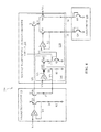
- FIG. 3 , FIG. 4 , and FIG. 5 show differential current signal circuit 110 according to the invention, which provides differential pair of current output signals I 3 and I 4 that are linearly proportional to an input voltage signal V 1 within a voltage operating range Vrange from a minimum operating voltage Vmin to a maximum operating voltage Vmax, while eliminating the problems discussed above.
- Differential current signal circuit 110 according to embodiments of the invention provides differential pair of current output signals I 3 and I 4 with improved linearity and reduced susceptibility to process and temperature variations as compared to other circuits.
- Differential pair of current output signals I 3 and I 4 are also referred to as differential pair of current signals I 3 and I 4 in this document.
- FIG. 3 shows a block diagram of an embodiment of differential current signal circuit 110 according to the invention.
- FIG. 3 shows a block diagram of an embodiment of differential current signal circuit 110 according to the invention.
- FIG. 4 shows a schematic diagram of one embodiment of differential current signal circuit 110 of FIG. 3
- FIG. 5 shows the voltage-to-current transfer function of differential current signal circuit 110 of FIG. 4 . It is to be understood that circuit elements, connections and configurations other than the specific example embodiment shown in FIG. 4 can be used in differential current signal circuit 110 according to the invention.
- Differential current signal circuit 110 includes voltage to differential current converter circuit 130 , and correction circuit 120 , as shown in FIG. 3 and FIG. 4 .
- Voltage to differential current converter circuit 130 converts voltage input signal V 1 into a differential pair of current output signals I 3 and I 4 , where the differential pair of current output signals includes first end I 3 and second end I 4 .
- First end I 3 is the first end of differential pair of current output signals I 3 and I 4 .
- Second end I 4 is the second end of differential pair of current output signals I 3 and I 4 .
- differential pair of current output signals I 3 and I 4 are 180 degrees out of phase, but the invention is not limited in this aspect.
- differential pair of current output signals I 3 and I 4 are modified differential signals, and their phase difference is some number of degrees other than 180 degrees.
- Correction circuit 120 provides the capability to set and adjust the minimum operating voltage of voltage to differential current converter circuit 130 , and reduces the susceptibility of voltage to differential current converter circuit 130 to temperature and process variations.
- Voltage to differential current converter circuit 130 converts voltage input signal V 1 into differential pair of current output signals I 3 and I 4 according to the voltage-to-current transfer function shown in FIG. 5 .
- the X-axis of the graph shown in FIG. 5 represents voltage values of voltage input signal V 1 .
- the Y-axis represents the output current levels of differential pair of current output signals I 3 and I 4 .
- Differential pair of current output signals I 3 and I 4 are linearly proportional to voltage input signal V 1 throughout the voltage operating range Vrange, where Vrange has a voltage range from Vmin to Vmax, as shown in FIG. 5 .
- Vo is the voltage at which the current level of first end I 3 is equal to the current level of second end I 4 .
- the operating range Vrange is that range of voltage input signals V 1 within which differential pair of current output signal pairs I 3 and I 4 are linearly proportional to voltage input signal V 1 .
- Vmin is the voltage input signal V 1 which defines the lower end of Vrange.
- Vmax is the voltage input signal V 1 which defines the upper end of Vrange.
- First end I 3 is at minimum current level Imin in response to values of voltage input signal V 1 that are lower than Vmin, as shown in FIG. 5 .
- the current level of second end I 4 is at maximum current level Imax in response to values of voltage input signal V 1 that are lower than Vmin, as shown in FIG. 5 .
- voltage input signal V 1 reaches Vmin and increases from Vmin to Vmax throughout the voltage operating range Vrange
- the current level of second end I 4 decreases from Imax to Imin, where I 4 is linearly proportional to V 1 throughout this range.
- I 4 remains at minimum current level Imin. In this way differential pair of current output signals I 3 and I 4 are both linearly proportional to V 1 throughput the voltage operating range Vrange from minimum operating voltage Vmin to maximum operating voltage Vmax.
- Differential pair of current output signals I 3 and I 4 are linear through the entire voltage operating range Vrange from Vmin to Vmax, similar to the desired response indicated by line 106 and line 107 in FIG. 2 . Therefore voltage to differential current converter circuit 130 has a wide voltage operating range Vrange within which differential pair of current output signals I 3 and I 4 are linearly proportional to voltage input signal V 1 .
- FIG. 5 also illustrates that the embodiment of differential current signal circuit 110 according to the invention as shown in FIG. 3 and FIG. 4 has a voltage operating range Vrange that consists of all positive voltage values.
- Vmin is a positive voltage value that can be adjusted to be within the linear range of the power supply.
- voltage input signal V 1 rises above zero to a value equal to Vmin before differential pair of current output signals I 3 and I 4 are linearly proportional to V 1 .
- differential current signal circuit 110 has a positive minimum operating voltage Vmin. This allows differential current signal circuit 110 to avoid issues due to degraded power supply voltage levels when the voltage level approaches zero.
- Differential current signal circuit 110 also includes correction circuit 120 , as shown in FIG. 3 and FIG. 4 .
- Correction circuit 120 provides a bias voltage to voltage to differential current converter circuit 130 in the form of tracking bias signal V 9 .
- Correction circuit 120 provides tracking bias voltage V 9 and set minimum operating voltage signal I 7 to voltage to differential current converter circuit 130 in response to correction circuit 120 receiving correction input voltage V 7 .
- Set minimum operating voltage signal I 7 allows adjusting of the minimum operating voltage Vmin of voltage to differential current converter circuit 130 .
- Tracking bias voltage V 9 eliminates voltage offsets in the voltage operating range due to process and temperature variations.
- a voltage offset is the difference between the voltage value that generates a particular output current value, and the voltage value that by design was supposed to generate the particular current output value.
- Voltage offsets in a circuit result in the voltage operating range being moved along the X-axis of the voltage-to-current transfer function graph by the voltage offset value.
- Voltage to differential current converter circuit 130 includes current source transistor Q 1 as shown in FIG. 4 .
- Current source transistor Q 1 provides current source signal I 5 to source-coupled transistor M 3 and M 4 , which divide current source signal I 5 into differential pair of current output signals I 3 and I 4 .
- undesirable voltage operating range offset is eliminated in response to current source transistor Q 1 of voltage to differential current converter circuit 130 receiving tracking bias signal V 9 from correction circuit 120 , as will be explained in more detail shortly.
- Set minimum operating voltage signal I 7 provided by correction circuit 120 to voltage to differential current converter circuit 130 is used to set the minimum operating voltage Vmin of voltage to differential current converter circuit 130 , as will be explained in more detail shortly.
- the minimum operating voltage Vmin of voltage to differential current converter circuit 130 is adjusted in response to adjusting set minimum operating voltage signal I 7 .
- set minimum operating voltage signal I 7 as received by voltage to differential current converter circuit 130 eliminates voltage offset in the minimum operating voltage due to process and temperature variations.
- Correction circuit 120 provides tracking bias voltage V 9 and set minimum operating voltage signal I 7 to voltage to differential current converter circuit 130 , which allows adjusting of the minimum operating voltage Vmin of voltage to differential current converter circuit 130 and also eliminates voltage operating range offsets due to process and temperature variations of voltage to differential current converter circuit 130 .
- Voltage to differential current converter circuit 130 includes voltage to single-ended current converter circuit 140 , and single-ended current to differential current converter circuit 150 , as shown in FIG. 3 and FIG. 4 .
- Voltage to single-ended current converter circuit 140 converts voltage input signal V 1 into single-ended current signal I 2 , where I 2 is linearly proportional to V 1 within a voltage operating range from a minimum voltage level to a maximum voltage level.
- Single-ended current to differential current converter circuit 150 converts single-ended current signal I 2 into differential pair of current output signals I 3 and I 4 , where differential pair of current output signals I 3 and I 4 are linearly proportional to voltage input signal V 1 within a voltage operating range Vrange from minimum operating voltage Vmin to maximum operating voltage Vmax.
- Voltage to single-ended current converter circuit 140 includes voltage to linear current feedback loop circuit 142 , and current replication transistor M 2 , as shown in block diagram form in FIG. 6 and in one possible schematic embodiment in FIG. 7 .
- Voltage to linear current feedback loop circuit 142 generates current replication voltage V 2 in response to receiving voltage input signal V 1 .
- Current replication transistor M 2 generates single-ended current signal I 2 in response to receiving current replication voltage V 2 , where single-ended current signal I 2 is linearly proportional to voltage input signal V 1 within a voltage operating range from a minimum voltage level to a maximum voltage level. It is to be understood that circuit elements, connections, and configurations other than the specific schematic embodiment shown in FIG. 7 can be used in voltage to single-ended current converter circuit 140 according to the invention.
- voltage to linear current feedback loop circuit 142 includes first feedback amplifier A 1 , first feedback transistor M 1 , and converter resistor R 1 .
- First feedback amplifier A 1 , first feedback transistor M 1 , and converter resistor R 1 form a first feedback loop.
- First feedback amplifier A 1 , first feedback transistor M 1 , and converter resistor R 1 convert voltage input signal V 1 into single-ended interim current signal I 1 and current replication voltage V 2 .
- First feedback amplifier A 1 first input node 263 receives voltage input signal V 1 .
- First feedback amplifier second input node 264 is coupled to first end I 31 of converter resistor R 1 , and first feedback transistor M 1 drain node 273 .
- First feedback transistor M 1 source node is coupled to supply voltage Vdd.
- First feedback transistor M 1 gate node 272 is coupled to first feedback amplifier A 1 output node 265 .
- First feedback amplifier output node 265 outputs current replication voltage V 2 in response to first feedback amplifier A 1 first input node 263 receiving voltage input signal V 1 .
- supply voltage Vdd is two volts, but the invention is not limited in this aspect.
- the resistance value of R 1 is 20K ohms, but the invention is not limited in this aspect.
- Voltage to linear current feedback loop circuit 142 which includes first feedback amplifier A 1 , first feedback transistor M 1 , and converter resistor R 1 , converts voltage input signal V 1 into single-ended interim current signal I 1 according to a voltage-to-current transfer function give by
- I ⁇ ⁇ 1 V ⁇ ⁇ 1 * gm ⁇ ⁇ 1 * ⁇ Av ⁇ ⁇ 1 1 + ( R ⁇ ⁇ 1 * gm ⁇ ⁇ 1 * Av ⁇ ⁇ 1 ) , ( 1 )
- V 1 is the voltage value of voltage input signal V 1
- R 1 is the resistance value of converter resistor R 1
- gm 1 is the transconductance of first feedback transistor M 1
- Av 1 is the voltage gain of first feedback amplifier A 1 .
- R 1 *gm 1 *Av 1 is much greater than 1, so the voltage-to-current transfer function of voltage to linear current feedback loop circuit 142 can be reduced to
- voltage to linear current feedback loop circuit 142 includes a first feedback loop which generates single-ended interim current signal I 1 that is linearly proportional to voltage input signal V 1 .
- voltage to linear current feedback loop circuit generates single-ended interim current signal I 1 in response to receiving voltage input signal V 1 , where single-ended interim current signal I 1 is linearly proportional to voltage input signal V 1 .
- voltage to linear current feedback loop circuit generates current replication voltage V 2 in response to receiving voltage input signal V 1 .
- FIG. 4 and FIG. 7 are examples of one specific embodiment of voltage to linear current feedback loop circuit 142 .
- Other circuit elements, discrete, or integrated, can be used in other embodiments of voltage to linear current feedback loop circuit 142 according to the invention.
- other circuit elements and other forms of feedback loop circuits are used for voltage to linear current feedback loop circuit 142 .
- First feedback amplifier A 1 outputs current replication voltage V 2 to both first feedback transistor M 1 and current replication transistor M 2 , as shown in FIG. 4 and FIG. 7 .
- Current replication transistor M 2 is chosen in this embodiment to be the same type of transistor as first feedback transistor M 1 , such that current replication transistor M 2 outputs single-ended current signal I 2 in response to receiving current replication voltage V 2 , where single-ended current signal I 2 is a duplicate of interim current signal I 1 within a current operating range from a minimum operating current to a maximum operating current.
- Current replication transistor M 2 source node 254 receives the supply voltage.
- Current replication transistor M 2 drain node 256 outputs single-ended current signal I 2 in response to current replication transistor gate node 255 receiving current replication voltage V 2 .
- current replication transistor M 2 duplicates single-ended interim current signal I 1 as single-ended current signal I 2 , where single-ended current signal I 2 is equal to interim current signal I 1 within a current operating range from a minimum operating current to a maximum operating current. Since interim current signal I 1 is linearly proportional to input voltage signal V 1 , single-ended current signal I 2 is also linearly proportional to input voltage signal V 1 within the voltage operating range Vrange from minimum operating voltage Vmin to maximum operating voltage Vmax. In this way current replication transistor M 2 generates single-ended current signal I 2 in response to receiving current replication voltage V 2 , where single ended current signal I 2 is linearly proportional to voltage input signal V 1 within voltage operating range Vrange from minimum operating voltage Vmin to maximum operating voltage Vmax.
- current replication transistor M 2 is the same type of transistor as first feedback transistor M 1 , which results in single-ended current signal I 2 being equal to interim current signal I 1 .
- transistors M 1 and M 2 are not the same type of transistor, but their voltage-to-current transfer functions are linearly proportional to each other.
- the voltage-to-current transfer function of current replication transistor M 2 is linearly proportional to the voltage-to-current transfer function of first feedback transistor M 1 , such that I 2 is linearly proportional to I 1 .
- current replication transistor M 2 is a different type of transistor than first feedback transistor M 1 .
- first feedback transistor M 1 and/or current replication transistor M 2 are used for first feedback transistor M 1 and/or current replication transistor M 2 .
- voltage to single-ended current converter circuit 140 the voltage-to-current transfer functions of M 1 and M 2 are linearly proportional to each other, and therefore single-ended current signal I 2 is linearly proportional to interim current signal I 1 .
- Single-ended current to differential current converter circuit 150 converts single-ended current signal I 2 into differential pair of current output signals I 3 and I 4 , where I 3 and I 4 are linearly proportional to voltage input signal V 1 within a voltage operating range Vrange from Vmin to Vmax.
- Single-ended current to differential current converter circuit 150 converts single-ended current signal I 2 into differential pair of current output signals I 3 and I 4 , where I 3 and I 4 are linearly proportional to single-ended current signal I 2 within a current operating range from a minimum current level to a maximum current level.
- Single-ended current to differential current converter circuit 150 includes load mirror circuit 152 , and voltage to differential current converter circuit 154 as shown in block diagram form in FIG. 8 , and in one schematic embodiment in FIG. 4 and FIG. 9 .
- Load mirror circuit 152 converts single-ended current signal I 2 into load-mirrored voltage signal V 4 .
- load mirror circuit 152 includes load mirror transistor Q 2 .
- Load mirror transistor collector node 159 receives single-ended current signal I 2
- load mirror transistor base node 160 outputs load-mirrored voltage signal V 4 in response.
- Load mirror transistor Q 2 base node 160 and load mirror transistor collector node 159 are coupled together.
- Load mirror transistor Q 2 emitter node 161 is coupled to a current return path.
- Load mirror circuit 152 has a nonlinear current-to-voltage transfer function that in this embodiment is determined by the logarithmic impedance function of load mirror transistor Q 2 , given by
- V ⁇ ⁇ 4 Vt * ln ⁇ ( I ⁇ ⁇ 2 Is ) , ( 3 ) where Vt is the transistor thermal voltage and Is is the transistor scaling current.
- Load mirror circuit 152 outputs load-mirrored voltage signal V 4 in response to receiving single-ended current signal I 2 , where load-mirrored voltage signal V 4 is a nonlinear function of single-ended current signal I 2 .
- load mirror circuit 152 has an impedance that is linearly proportional to the impedance of load 168 that is seen by differential pair of current output signals I 3 and I 4 .
- load mirror transistor Q 2 is the same type of transistor as load transistors Q 4 and Q 5 that are seen by differential pair of current output signals I 3 and I 4 .
- differential pair of current output signal first end I 3 sees load transistor Q 4 as shown in FIG. 9 .
- Differential pair of current output signals second end I 4 sees load transistor Q 5 in the embodiment shown in FIG. 9 .
- load mirror transistor Q 2 is the same type of transistor as load transistor Q 4 and load transistor Q 5 .
- load mirror circuit 152 is a transistor of a different type than load transistors Q 4 and Q 5 , where load mirror transistor Q 2 has an impedance that is linearly proportional to load transistors Q 4 and Q 5 .
- load mirror circuit 152 is a circuit which has an impedance that is linearly proportional to load transistors Q 4 and Q 5 .
- load mirror circuit 152 has a current-to-voltage transfer function that is linearly proportional to the current-to-voltage transfer function of Q 4 and Q 5 .
- Voltage to differential current converter circuit 154 converts load-mirrored voltage signal V 4 into differential pair of current output signals I 3 and I 4 , where differential pair of current output signals I 3 and I 4 are linearly proportional to single-ended current signal I 2 within a current operating range from a minimum operating current to a maximum operating current.
- Voltage to differential current converter circuit 154 converts load-mirrored voltage signal V 4 into differential pair of current output signals I 3 and I 4 , where differential pair of current output signals I 3 and I 4 are linearly proportional to voltage input signal V 1 within a voltage operating range Vrange from minimum operating voltage Vmin to maximum operating voltage Vmax, as shown in FIG. 4 , FIG. 5 , FIG. 8 , and FIG. 9 .
- Voltage to differential current converter circuit 154 includes second feedback amplifier A 2 and source-coupled amplifier circuit 156 .
- Second feedback amplifier A 2 generates second feedback amplifier output voltage V 8 in response to receiving load-mirrored voltage signal V 4 .
- Source-coupled amplifier circuit 156 generates differential pair of current output signals I 3 and I 4 in response to receiving second feedback amplifier output voltage V 8 , tracking bias signal V 9 , and bias voltage V 6 , as shown in the figures.
- Differential pair of current output signals I 3 and I 4 are provided to load circuit 168 .
- load circuit 168 includes load transistors Q 4 and Q 5 .
- differential pair of current output signals first end I 3 sees load transistor Q 4
- differential pair of current output signals second end I 4 sees load transistor Q 5 .
- load transistor Q 4 and load transistor Q 5 are both the same type of transistor as load mirror transistor Q 2 , and so the impedance of load mirror circuit 152 is equal to the impedance of load transistor Q 4 and the impedance of load transistor Q 5 .
- the impedance of load transistor Q 4 , load transistor Q 5 , and load mirror circuit 152 are linearly proportional to one another.
- the impedance of load mirror circuit 152 is linearly proportional to load circuit 168 as seen by differential pair of current output signals I 3 and I 4 .
- Source-coupled amplifier circuit 156 includes current source transistor Q 1 , first source-coupled transistor M 3 , and second source-coupled transistor M 4 , as shown in FIG. 9 .
- Source-coupled amplifier circuit 156 generates differential pair of current output signals I 3 and I 4 in response to receiving bias voltages at the base nodes of current source transistor Q 1 , first source-coupled transistor M 3 , and second source-coupled transistor M 4 .
- Source-coupled amplifier circuit 156 converts the difference in voltages as seen by the gate nodes 184 and 188 of M 3 and M 4 respectively into differential pair of current output signals I 3 and I 4 .
- Q 1 base node 178 would receive a bias voltage
- transistors M 3 and M 4 would convert the difference between the bias voltages of transistors M 3 and M 4 into a differential pair of current output signals according to a nonlinear voltage-to-current function given by lines 104 and 105 of FIG. 2 , where the X-axis would be the voltage difference at the base node of M 3 and M 4 , line 104 would represent the first end of the differential pair of current output signals, and line 105 would represent the second end of the differential pair of current output signals.
- voltage to differential current converter circuit 154 adds novel features described herein to source-coupled amplifier circuit 156 to improve the linearity of the output signals and widen the voltage operating range.
- voltage to differential current converter circuit 156 One feature of voltage to differential current converter circuit 156 is that current source transistor Q 1 base node 178 receives tracking bias signal V 9 as its bias voltage. Receiving tracking bias signal V 9 at current source transistor base node 178 provides voltage to differential current converter circuit 130 the capability to eliminate offsets in the voltage operating range due to variations in the resistance value of R 1 and R 2 . This capability will be discussed in more detail shortly.
- Second feedback loop 151 includes second feedback loop amplifier A 2 , first source-coupled transistor M 3 , and first load transistor Q 4 , as shown in the dotted line box in FIG. 9 .
- the voltage-to-current transfer function of feedback loop 151 according to the invention is nonlinear, and is inversely proportional to the current-to-voltage transfer function of load mirror circuit 152 when the impedance of load mirror circuit 152 is linearly proportional to the impedance of load transistor Q 4 .
- second feedback loop amplifier A 2 first input node 171 receives load-mirrored voltage signal V 4 , where load-mirrored voltage signal is generated by load mirror circuit 152 .
- First source-coupled transistor M 3 gate node 184 receives second feedback amplifier output voltage V 8 from second feedback amplifier output node 173 .
- First source-coupled transistor M 3 drain node 185 is coupled to second feedback loop amplifier A 2 second input node 172 and first load transistor Q 4 collector and base nodes.
- Feedback loop circuit 151 defines the voltage-to-current transfer function of voltage to differential current converter circuit 154 for the generation of differential pair of current output signals first end I 3 .
- first load transistor Q 4 has the same impedance function as load mirror transistor Q 2
- the voltage-to-current transfer function of voltage to differential current converter circuit 154 defining the generation of differential pair of current output signals first end I 3 is inversely proportional to the current-to-voltage transfer function of load mirror circuit 152 .
- load mirror circuit 152 converts single-ended current signal I 2 into load-mirrored voltage signal V 4 according to a current-to-voltage transfer function given by equation 3
- voltage to differential current converter circuit 154 converts load-mirrored voltage signal V 4 into differential pair of current output signals first end I 3 according to a voltage-to current-transfer function that is inversely proportional to the current-to-voltage transfer function of load mirror circuit 152 .
- first load transistor Q 4 has the same impedance function as load mirror transistor Q 2
- differential pair of current output signals first end I 3 is equal to single-ended current signal I 2 .
- load mirror circuit 152 given by load mirror transistor Q 2 has an impedance that is not equal to, but linearly proportional to, the impedance of load transistor Q 4 .
- first load transistor Q 4 has an impedance function that is linearly proportional to the impedance of load mirror transistor Q 2
- differential pair of current output signals first end I 3 is linearly proportional to single-ended current signal I 2 .
- second feedback loop 151 forces first end of differential pair of current output signals I 3 to be linearly proportional to single-ended current signal I 2 within the current operating range of single-ended current signal I 2 .
- second feedback loop 151 generates first end of differential pair of current output signals I 3 , where first end of differential pair of current output signals I 3 is equal to single-ended current signal I 2 , when the impedance of load mirror circuit 152 is equal to the impedance of load 168 as seen by first end of differential pair of current output signals I 3 .
- Second feedback loop 151 generates first end of differential pair of current output signals I 3 , where first end of differential pair of current output signals I 3 is equal to single-ended current signal I 2 , when the impedance of load mirror transistor Q 2 is equal to the impedance of load transistor Q 4 as seen by first end of differential pair of current output signals I 3 .
- Second feedback loop 151 generates first end of differential pair of current output signals I 3 , where first end of differential pair of current output signals I 3 is linearly proportional to single-ended current signal I 2 , when the impedance of load mirror circuit 152 is linearly proportional to the impedance of load 168 as seen by first end of differential pair of current output signals I 3 .
- First end of differential pair of current output signal I 3 is linearly proportional to single-ended current signal I 2 in response to the impedance of load mirror circuit 152 being linearly proportional to the impedance of load 168 as seen by first end of differential pair of current output signals I 3 .
- the level of linear proportionality between the nonlinear impedance functions of load mirror circuit 152 and load 168 as seen by I 3 will determine the level of linearity between first end of differential pair of current output signals I 3 and single-ended current signal I 2 (and therefore between first end of differential pair of current output signals I 3 and interim current signal I 1 and between first end of differential pair of current output signals I 3 and voltage input signal V 1 ).
- voltage to differential current converter circuit 154 generates first end of differential pair of current output signals I 3 from load-mirrored voltage signal V 4 using second feedback loop circuit 151 .
- Voltage to differential current converter circuit 154 generates first end of differential pair of current output signals I 3 from load-mirrored voltage signal V 4 , where first end of differential pair of current output signal I 3 is linearly proportional to voltage input signal V 1 within voltage operating range Vrange from minimum operating voltage Vmin to maximum operating voltage Vmax in response to the impedance of load mirror transistor Q 2 being linearly proportional to the impedance of load 168 that is receiving first end of differential pair of current output signal I 3
- Second source-coupled amplifier M 4 generates differential pair of current output signals second end I 4 according to equation 4 at second source-coupled amplifier M 4 gate node 189 .
- Differential pair of current output signal second end I 4 is 180 degrees out of phase from differential pair of current output signals first end I 3 .
- Differential pair of current output signals I 3 and I 4 are generated according to the voltage-to-current transfer function as shown in FIG. 5 , where V 1 is voltage input signal V 1 .
- Differential pair of current output signals I 3 and I 4 are linearly proportional to V 1 within a range of operating voltages Vrange from Vmin to Vmax.
- V 7 is equal to V 6 .
- V 6 and V 7 are not the same voltage value.
- source voltage Vdd is 2 volts
- correction input voltage V 7 is the same as bias voltage V 6 which is 1 volt
- Vo is equal to 1 volt.
- the resistance value of R 1 is 20K ohms
- the resistance value of R 2 is 10K ohms.
- This specific embodiment of differential current signal circuit 110 according to the invention leads to Vmin being equal to 500 millivolts, and Vmax being equal to 1.5 volts, which means that the voltage operating range Vrange (see FIG. 5 ) is equal to 1 volt.
- Imin is zero amps
- Imax is equal to 100 microamps. It is to be understood that this is one specific example embodiment and that the circuit is not limited to these example values.
- single-ended current to differential current converter circuit 150 outputs differential pair of current output signal I 3 and I 4 in response to receiving single-ended current signal I 2 , where differential pair of current output signals I 3 and I 4 are linearly proportional to single-ended current signal I 2 within a range of operating current values from Imin to Imax.
- Single-ended current signal I 2 is linearly proportional to interim current signal I 1 within the range of current values from Imin to Imax.
- Interim current signal I 1 is linearly proportional to voltage input signal V 1 within the voltage operating range from Vmax to Vmin.
- Differential pair of current output signals I 3 and I 4 are linearly proportional to input voltage signal V 1 within an operating range Vrange from a minimum operating voltage Vmin to a maximum operating voltage Vmax as shown in FIG.
- voltage to differential current converter circuit 130 outputs differential pair of current output signal I 3 and I 4 in response to receiving voltage input signal V 1 , where differential pair of current output signals I 3 and I 4 are linearly proportional to voltage input signal V 1 within voltage operating range Vrange from minimum operating voltage Vmin to maximum operating voltage Vmax.
- Differential current signal circuit 110 also includes correction circuit 120 , as shown in FIG. 3 , FIG. 4 , and FIG. 10 .
- Correction circuit 120 provides differential current signal circuit 110 the capability to set and adjust the minimum operating voltage of voltage to differential current converter circuit 130 , and reduces the susceptibility of voltage to differential current converter circuit 130 to temperature and process variations.
- Correction circuit 120 is shown in one possible schematic embodiment in FIG. 4 and FIG. 10 . In some embodiments correction circuit 120 is implemented with other circuit elements.
- Correction circuit 120 generates tracking bias voltage V 9 and set minimum operating voltage signal I 7 in response to receiving correction input voltage V 7 .
- second source-coupled transistor M 4 receives bias voltage V 6 at gate node 188 .
- the bias voltage provided to current source transistor Q 1 base node 178 is tracking bias signal V 9 , where tracking bias signal V 9 is generated by correction circuit 120 in response to receiving correction input voltage V 7 .
- Correction circuit 120 includes a third feedback loop, where the third feedback loop includes tracking bias amplifier A 3 , tracking bias transistor Q 3 , and tracking bias resistor R 2 .
- Tracking bias amplifier first input node 232 receives correction input voltage V 7 .
- Tracking bias amplifier second input node 234 is coupled to tracking bias transistor Q 3 collector node 226 and first end 127 of tracking bias resistor R 2 .
- Tracking bias amplifier output node 236 outputs tracking bias signal V 9 . Therefore the amplitude of tracking bias signal V 9 is a function of the resistance value of R 2 .
- Tracking bias amplifier output node 236 is coupled to tracking bias transistor base node 224 .
- Tracking bias transistor Q 3 emitter node 222 receives the supply voltage. Tracking bias amplifier A 3 , tracking bias transistor Q 3 , and tracking bias resistor R 2 create tracking bias current I 6 , given by
- Equation 5 for I 6 is derived similarly to interim current signal I 1 earlier. Therefore the amplitude of tracking bias current I 6 , and the amplitude of tracking bias signal V 9 output from tracking bias amplifier A 3 are both a function of the resistance value of R 2 .
- Tracking bias signal V 9 is received by current source transistor Q 1 base node 178 .
- Q 1 and Q 3 are chosen to be the same type of transistor, therefore I 5 is equal to I 6 .
- Current signals I 1 , I 2 , and I 3 and are all derived from the resistance value of R 1 , as discussed earlier.
- resistors R 1 and R 2 are made by the same process, and so their resistance values will vary proportionally to each other due to process variations and temperature variations.
- resistor R 2 is chosen to have a resistance value that is half the resistance value of R 1 , but the invention is not limited in this aspect.
- Correction circuit 120 eliminates voltage range offsets and output signal variation due to process and temperature-related resistance value variations because resistor R 1 and R 2 are made by the same process and their resistance values will vary proportionally to one another.
- current source signal I 5 is derived from the resistance value of tracking bias resistor R 2 .
- Variations in the resistance value of R 2 due to process or temperature variations could cause the voltage operating range Vrange to be offset from its desired value by some voltage offset amount. This can result in a desired current value for differential pair of current output signals I 3 and I 4 requiring a voltage input value that is offset from the expected input value. It may be important, for example, to know the voltage value of Vo, where the current level of I 3 and I 4 are equal to one another.
- Correction circuit 120 also provides set minimum operating voltage signal I 7 to voltage to differential current converter circuit 130 , as shown in FIG. 3 and FIG. 4 .
- Correction circuit 120 generates set minimum operating voltage signal I 7 in response to receiving correction input voltage V 7 , as shown in FIG. 10 .
- Set minimum operating voltage transistor Q 6 collector node 246 outputs set minimum operating voltage signal I 7 in response to set minimum operating voltage transistor Q 6 base node 242 receiving tracking bias signal V 9 .
- Set minimum operating voltage transistor Q 6 emitter node 244 receives the supply voltage Vdd.
- Set minimum operating voltage transistor Q 6 collector node 246 is coupled to first end I 31 of converter resistor R 1 as shown in FIG. 4 and FIG. 7 .
- This circuit arrangement means that interim current signal I 1 will be zero until voltage input signal V 1 rises above the minimum operating voltage Vmin, where Vmin is given by
- V ⁇ ⁇ min ( R ⁇ ⁇ 1 * Vo R ⁇ ⁇ 2 ) * q ⁇ ⁇ 6 q ⁇ ⁇ 3 , ( 6 ) where q 6 /q 3 is the transistor emitter ratio of transistors Q 6 and Q 3 .
- the minimum operating voltage Vmin of voltage to differential current converter circuit 130 is adjusted by adjusting 17 , which is adjusted by adjusting the elements in equation 6. In this way correction circuit 120 outputs set minimum operating voltage signal I 7 in response to receiving correction input voltage V 7 , where minimum operating voltage Vmin is adjusted in response to adjusting set minimum operating voltage signal I 7 .
- Providing set minimum operating voltage signal I 7 to voltage to differential current converter circuit 130 allows the minimum operating voltage Vmin of voltage to differential current converter circuit 130 to be set at a level above zero, such that the operating range Vrange of voltage to differential current converter circuit 130 will be all positive values as shown in FIG. 5 .
- This circuit arraignment also allows Vmin to be set a voltage value away from the voltage supply rails where nonlinear behavior sometimes occurs.
- set minimum operating voltage signal I 7 will correct voltage offsets in minimum operating voltage Vmin for variations due to processing and temperature variations in the resistance value of converter resistor R 1 and/or the resistance value of tracking bias resistor R 2 .
- Tracking bias resistor R 2 will vary due to variations in process and temperature proportionally to converter resistor R 1 , because the two resistors are made by the same process. Therefore, variations in the resistance value of converter resistor R 1 and tracking bias resistor R 2 will cancel each other, allowing Vmin to remain stable over temperature and process variations. In this way variations in minimum operating voltage Vmin due to variations in the resistance value of converter resistor R 1 or tracking bias resistor R 2 from process and temperature variations are eliminated in response to voltage to differential current converter circuit 130 receiving set minimum operating voltage signal I 7 .
- Converter circuit 120 can be implements using circuit elements other than those shown in the specific schematic example embodiments shown in FIG. 4 and FIG. 10 . In some embodiments circuit elements different than those in the figures are used. In some embodiments connections or configurations different than those shown in the figures are used for correction circuit 120 according to the invention.
- differential current signal circuit 110 as shown in the specific schematic embodiments can be implemented in many different ways. Circuit elements other than those shown in the figures can be used. In some embodiments different types of transistors can be implemented. In some embodiments other integrated or discrete circuit elements are used. Differential current signal circuit 110 according to the invention can be embodied in many different specific circuit designs and implementations.
- FIG. 11 shows method 300 of generating a differential pair of current signals according to the invention.
- Method 300 includes step 310 providing a single-ended current signal to a load mirror transistor, wherein the load mirror transistor outputs a load-mirrored voltage signal in response to receiving the single-ended current signal, and wherein the load-mirrored voltage signal is a nonlinear function of the single-ended current signal.
- Step 310 can include many other steps.
- Method 300 also includes step 320 generating a differential pair of current signals from the load-mirrored voltage signal, wherein a first end of the differential pair of current signals is linearly proportional to the single-ended current signal within an operating range from a minimum current level to a maximum current level.
- the first end of the differential pair of current signals is linearly proportional to the single-ended current signal within an operating range from a minimum current level to a maximum current level in response to the impedance of the load mirror circuit being linearly proportional to the impedance of a load circuit as seen by the first end of the differential pair or current output signals.
- Step 320 can include many other steps.
- Method 300 can include many other steps.
- method 300 includes the step of providing the first end of the differential pair of current signals to a first load transistor, and the step of providing a second end of the differential pair of current signals to a second load transistor, wherein the first load transistor, the second load transistor, and the load mirror circuit have the same impedance.
- method 300 includes the step of generating the single-ended current signal with a voltage to single-ended current converter circuit, wherein the voltage to single-ended current converter circuit generates the single-ended current signal in response to receiving a voltage input signal, and wherein the single-ended current signal is linearly proportional to the voltage input signal within a voltage operating range from a minimum operating voltage to a maximum operating voltage.
- the voltage to single-ended current converter circuit includes a converter resistor.
- method 300 includes the step of generating a tracking bias signal with a correction circuit, where voltage offsets in the voltage operating range due to variations in the resistance value of the converter resistor are eliminated in response to the voltage to single-ended current converter circuit receiving the tracking bias signal.
- the correction circuit includes a tracking bias resistor, and the amplitude of the tracking bias signal is a function of the resistance value of the tracking bias resistor. In some embodiments the correction circuit outputs a set minimum operating voltage signal, and the minimum operating voltage of the voltage to single-ended current converter circuit is adjusted in response to adjustments to the set minimum operating voltage signal.
- FIG. 12 shows method 400 of generating a differential pair of current signals according to the invention.
- Method 400 of generating a differential pair of current signals includes step 410 generating a first single-ended current signal that is linearly proportional to a voltage input signal using a first feedback loop, and step 420 duplicating the first single-ended current signal to create a second single-ended current signal.
- Method 400 of generating a differential pair of current signals according to the invention also includes step 430 generating a load-mirrored voltage signal from the second single-ended current signal using a load mirror circuit, wherein the load-mirrored voltage signal is nonlinearly proportional to the second single-ended current signal.
- Method 400 also includes step 440 of generating a first end of a differential pair of current signals from the load-mirrored voltage signal using a second feedback loop, where the first end of the differential pair of current signals is linearly proportional to the voltage input signal within a voltage operating range from a minimum operating voltage to a maximum operating voltage
- Method 400 can include many other steps, In some embodiments method 400 includes the step of generating a second end of the differential pair of current signals, wherein the second end of the differential pair of current signals has a phase that is shifted 180 degrees with respect to a phase of the first end of the differential pair of current signals In some embodiments method 400 includes the step of generating a set minimum operating voltage signal, wherein the minimum operating voltage is adjusted in response to adjusting the set minimum operating voltage signal. In some embodiments voltage offsets in the voltage operating range due to process or temperature variations are eliminated in response to the first feedback loop circuit receiving the set minimum operating voltage signal.
- Step 420 can include many other steps.
- the second single-ended current signal is generated using a current replication transistor.
- Step 430 generating a load-mirrored voltage signal from the second single-ended current signal using a load mirror circuit, wherein the load-mirrored voltage signal is nonlinearly proportional to the second single-ended current signal, can include many other steps.
- the load mirror circuit is a transistor, and the load-mirrored voltage signal is nonlinearly proportional to the single ended current signal.
- the impedance of the load mirror circuit is the same as the impedance of a first load transistor, wherein the first load transistor receives the first end of the differential pair of current signals.
- voltage to differential current converter circuit 130 generates a differential pair of current output signals I 3 and I 4 in response to receiving a voltage input signal V 1 , where differential pair of current output signals I 3 and I 4 are linearly proportional to voltage input signal V 1 within a voltage operating range Vrange from a minimum operating voltage Vmin to a maximum operating voltage Vmax. It has been shown how voltage to differential current converter circuit 130 provides a voltage operating range Vrange that provides linear output signals I 3 and I 4 over a wide range of voltage input signals V 1 .
- correction circuit 120 in current signal source circuit 110 allows the elimination of voltage offsets in the voltage operating range from variations in the resistance value of converter resistor R 1 and/or tracking bias resistor R 2 that are used in the generation of differential pair of current output signals I 3 and I 4 .
Landscapes
- Engineering & Computer Science (AREA)
- Power Engineering (AREA)
- Physics & Mathematics (AREA)
- Electromagnetism (AREA)
- General Physics & Mathematics (AREA)
- Radar, Positioning & Navigation (AREA)
- Automation & Control Theory (AREA)
- Amplifiers (AREA)
Abstract
Description
where V1 is the voltage value of voltage input signal V1, R1 is the resistance value of converter resistor R1, gm1 is the transconductance of first feedback transistor M1 and Av1 is the voltage gain of first feedback amplifier A1. In this embodiment R1*gm1*Av1 is much greater than 1, so the voltage-to-current transfer function of voltage to linear current
Since equation 2 is highly linear, single-ended interim current signal I1 is linearly proportional to voltage input signal V1. In this way voltage to linear current
where Vt is the transistor thermal voltage and Is is the transistor scaling current.
I5=I3+I4. (4)
In a traditional source-coupled amplifier circuit (see
where V7 is equal to the voltage value of correction input voltage V7, and R2 is the resistance value of tracking bias resistor R2. Equation 5 for I6 is derived similarly to interim current signal I1 earlier. Therefore the amplitude of tracking bias current I6, and the amplitude of tracking bias signal V9 output from tracking bias amplifier A3 are both a function of the resistance value of R2.
where q6/q3 is the transistor emitter ratio of transistors Q6 and Q3. The minimum operating voltage Vmin of voltage to differential
Claims (24)
Priority Applications (2)
| Application Number | Priority Date | Filing Date | Title |
|---|---|---|---|
| US13/089,859 US8441288B2 (en) | 2011-04-19 | 2011-04-19 | Differential current signal circuit |
| US13/859,366 US8614593B2 (en) | 2011-04-19 | 2013-04-09 | Differential current signal circuit |
Applications Claiming Priority (1)
| Application Number | Priority Date | Filing Date | Title |
|---|---|---|---|
| US13/089,859 US8441288B2 (en) | 2011-04-19 | 2011-04-19 | Differential current signal circuit |
Related Child Applications (1)
| Application Number | Title | Priority Date | Filing Date |
|---|---|---|---|
| US13/859,366 Continuation US8614593B2 (en) | 2011-04-19 | 2013-04-09 | Differential current signal circuit |
Publications (2)
| Publication Number | Publication Date |
|---|---|
| US20120268169A1 US20120268169A1 (en) | 2012-10-25 |
| US8441288B2 true US8441288B2 (en) | 2013-05-14 |
Family
ID=47020829
Family Applications (2)
| Application Number | Title | Priority Date | Filing Date |
|---|---|---|---|
| US13/089,859 Active 2031-09-16 US8441288B2 (en) | 2011-04-19 | 2011-04-19 | Differential current signal circuit |
| US13/859,366 Active US8614593B2 (en) | 2011-04-19 | 2013-04-09 | Differential current signal circuit |
Family Applications After (1)
| Application Number | Title | Priority Date | Filing Date |
|---|---|---|---|
| US13/859,366 Active US8614593B2 (en) | 2011-04-19 | 2013-04-09 | Differential current signal circuit |
Country Status (1)
| Country | Link |
|---|---|
| US (2) | US8441288B2 (en) |
Cited By (1)
| Publication number | Priority date | Publication date | Assignee | Title |
|---|---|---|---|---|
| US8614593B2 (en) * | 2011-04-19 | 2013-12-24 | Sand 9, Inc. | Differential current signal circuit |
Families Citing this family (2)
| Publication number | Priority date | Publication date | Assignee | Title |
|---|---|---|---|---|
| JP6471619B2 (en) * | 2015-06-12 | 2019-02-20 | 株式会社デンソー | Electronic equipment |
| CN112910605B (en) * | 2021-02-18 | 2023-03-24 | 联想(北京)有限公司 | Signal adjusting method and device and electronic equipment |
Citations (5)
| Publication number | Priority date | Publication date | Assignee | Title |
|---|---|---|---|---|
| US5068621A (en) * | 1990-08-13 | 1991-11-26 | Triquint Semiconductor, Inc. | Compensation method and apparatus for enhancing single-ended to differential conversion |
| US5963064A (en) * | 1997-01-17 | 1999-10-05 | Hitachi, Ltd. | Linear transfer voltage to current circuit |
| US6566961B2 (en) * | 2001-03-30 | 2003-05-20 | Institute Of Microelectronics | Wide-band single-ended to differential converter in CMOS technology |
| US7688146B2 (en) * | 2006-03-01 | 2010-03-30 | Princeton Technology Corporation | Single-ended input to differential-ended output low noise amplifier |
| US8320149B2 (en) * | 2010-02-04 | 2012-11-27 | Richtek Technology Corporation, R.O.C. | Multi-chip module with master-slave analog signal transmission function |
Family Cites Families (1)
| Publication number | Priority date | Publication date | Assignee | Title |
|---|---|---|---|---|
| US8441288B2 (en) * | 2011-04-19 | 2013-05-14 | Sand 9, Inc. | Differential current signal circuit |
-
2011
- 2011-04-19 US US13/089,859 patent/US8441288B2/en active Active
-
2013
- 2013-04-09 US US13/859,366 patent/US8614593B2/en active Active
Patent Citations (5)
| Publication number | Priority date | Publication date | Assignee | Title |
|---|---|---|---|---|
| US5068621A (en) * | 1990-08-13 | 1991-11-26 | Triquint Semiconductor, Inc. | Compensation method and apparatus for enhancing single-ended to differential conversion |
| US5963064A (en) * | 1997-01-17 | 1999-10-05 | Hitachi, Ltd. | Linear transfer voltage to current circuit |
| US6566961B2 (en) * | 2001-03-30 | 2003-05-20 | Institute Of Microelectronics | Wide-band single-ended to differential converter in CMOS technology |
| US7688146B2 (en) * | 2006-03-01 | 2010-03-30 | Princeton Technology Corporation | Single-ended input to differential-ended output low noise amplifier |
| US8320149B2 (en) * | 2010-02-04 | 2012-11-27 | Richtek Technology Corporation, R.O.C. | Multi-chip module with master-slave analog signal transmission function |
Non-Patent Citations (1)
| Title |
|---|
| Wyszynski, A.; , "High-frequency linear tunable single-ended voltage to differential current converter," Circuits and Systems, 1995., Proceedings., Proceedings of the 38th Midwest Symposium on , vol. 2, no., pp. 897-900 vol. 2, Aug. 13-16, 1995. * |
Cited By (1)
| Publication number | Priority date | Publication date | Assignee | Title |
|---|---|---|---|---|
| US8614593B2 (en) * | 2011-04-19 | 2013-12-24 | Sand 9, Inc. | Differential current signal circuit |
Also Published As
| Publication number | Publication date |
|---|---|
| US20130222014A1 (en) | 2013-08-29 |
| US20120268169A1 (en) | 2012-10-25 |
| US8614593B2 (en) | 2013-12-24 |
Similar Documents
| Publication | Publication Date | Title |
|---|---|---|
| US9285822B2 (en) | Small-circuit-scale reference voltage generating circuit | |
| US7642814B2 (en) | Leakage compensation circuit using limiting current inverter | |
| TWI571723B (en) | Circuit for a current having a programmable temperature slope | |
| EP2480947A1 (en) | Compensated bandgap | |
| US20080191673A1 (en) | Series regulator circuit | |
| US7625118B2 (en) | Circuit for correcting sensor temperature characteristics | |
| US20060284659A1 (en) | Cmos integrated circuit for correction of duty cycle of clock signal | |
| US8614593B2 (en) | Differential current signal circuit | |
| NL8006006A (en) | AMPLIFICATION CONTROL CHAIN. | |
| CN109960309B (en) | Current generating circuit | |
| US9780736B1 (en) | Temperature compensated offset cancellation for high-speed amplifiers | |
| US9740232B2 (en) | Current mirror with tunable mirror ratio | |
| JP6270002B2 (en) | Pseudo resistance circuit and charge detection circuit | |
| US7859339B2 (en) | Differential amplification circuit | |
| CN117200713A (en) | Meter amplifier | |
| CN110690878A (en) | Method for biasing the output of a folded cascode stage in a comparator and corresponding comparator | |
| CN108345336B (en) | Energy gap reference circuit | |
| CN107786185B (en) | Phase interpolator | |
| CN111064453B (en) | Voltage comparator | |
| CN112346505B (en) | Gain modulation circuit | |
| JP6357182B2 (en) | Sensor device | |
| KR100599974B1 (en) | Voltage reference generator | |
| US20240291441A1 (en) | Bias voltage generating circuit, signal generator circuit and power amplifier | |
| TWI830582B (en) | Oscillator and method and thermally compensated circuit for tuning oscillator | |
| WO2023032608A1 (en) | Power amplifier |
Legal Events
| Date | Code | Title | Description |
|---|---|---|---|
| AS | Assignment |
Owner name: SAND 9, INC., MASSACHUSETTS Free format text: ASSIGNMENT OF ASSIGNORS INTEREST;ASSIGNORS:BADILLO, DEAN A.;LOCASCIO, DAVID R.;REEL/FRAME:026153/0178 Effective date: 20110325 |
|
| STCF | Information on status: patent grant |
Free format text: PATENTED CASE |
|
| AS | Assignment |
Owner name: ANALOG DEVICES, INC., MASSACHUSETTS Free format text: ASSIGNMENT OF ASSIGNORS INTEREST;ASSIGNOR:SAND 9, INC.;REEL/FRAME:036274/0273 Effective date: 20150515 |
|
| FEPP | Fee payment procedure |
Free format text: PAT HOLDER NO LONGER CLAIMS SMALL ENTITY STATUS, ENTITY STATUS SET TO UNDISCOUNTED (ORIGINAL EVENT CODE: STOL); ENTITY STATUS OF PATENT OWNER: LARGE ENTITY |
|
| FPAY | Fee payment |
Year of fee payment: 4 |
|
| MAFP | Maintenance fee payment |
Free format text: PAYMENT OF MAINTENANCE FEE, 8TH YEAR, LARGE ENTITY (ORIGINAL EVENT CODE: M1552); ENTITY STATUS OF PATENT OWNER: LARGE ENTITY Year of fee payment: 8 |