US8421924B2 - Image processing circuit and image processing method - Google Patents
Image processing circuit and image processing method Download PDFInfo
- Publication number
- US8421924B2 US8421924B2 US12/685,384 US68538410A US8421924B2 US 8421924 B2 US8421924 B2 US 8421924B2 US 68538410 A US68538410 A US 68538410A US 8421924 B2 US8421924 B2 US 8421924B2
- Authority
- US
- United States
- Prior art keywords
- chromaticity
- chroma
- image signal
- luminosity
- difference
- Prior art date
- Legal status (The legal status is an assumption and is not a legal conclusion. Google has not performed a legal analysis and makes no representation as to the accuracy of the status listed.)
- Active, expires
Links
- 238000003672 processing method Methods 0.000 title claims abstract description 61
- 238000000034 method Methods 0.000 claims abstract description 35
- 238000001914 filtration Methods 0.000 claims abstract description 27
- 241000023320 Luma <angiosperm> Species 0.000 claims description 63
- OSWPMRLSEDHDFF-UHFFFAOYSA-N methyl salicylate Chemical compound COC(=O)C1=CC=CC=C1O OSWPMRLSEDHDFF-UHFFFAOYSA-N 0.000 claims description 63
- -1 detecting module Chemical compound 0.000 claims 2
- 238000009826 distribution Methods 0.000 description 15
- 230000002159 abnormal effect Effects 0.000 description 14
- 238000010586 diagram Methods 0.000 description 11
- 230000015572 biosynthetic process Effects 0.000 description 6
- 239000003086 colorant Substances 0.000 description 6
- 230000000694 effects Effects 0.000 description 2
- 238000012986 modification Methods 0.000 description 2
- 230000004048 modification Effects 0.000 description 2
- 239000002131 composite material Substances 0.000 description 1
- 230000010355 oscillation Effects 0.000 description 1
- 238000009877 rendering Methods 0.000 description 1
- 230000000717 retained effect Effects 0.000 description 1
- 238000001228 spectrum Methods 0.000 description 1
Images


Classifications
-
- H—ELECTRICITY
- H04—ELECTRIC COMMUNICATION TECHNIQUE
- H04N—PICTORIAL COMMUNICATION, e.g. TELEVISION
- H04N5/00—Details of television systems
- H04N5/14—Picture signal circuitry for video frequency region
- H04N5/142—Edging; Contouring
-
- H—ELECTRICITY
- H04—ELECTRIC COMMUNICATION TECHNIQUE
- H04N—PICTORIAL COMMUNICATION, e.g. TELEVISION
- H04N9/00—Details of colour television systems
- H04N9/64—Circuits for processing colour signals
- H04N9/646—Circuits for processing colour signals for image enhancement, e.g. vertical detail restoration, cross-colour elimination, contour correction, chrominance trapping filters
-
- H—ELECTRICITY
- H04—ELECTRIC COMMUNICATION TECHNIQUE
- H04N—PICTORIAL COMMUNICATION, e.g. TELEVISION
- H04N9/00—Details of colour television systems
- H04N9/64—Circuits for processing colour signals
- H04N9/66—Circuits for processing colour signals for synchronous demodulators
-
- H—ELECTRICITY
- H04—ELECTRIC COMMUNICATION TECHNIQUE
- H04N—PICTORIAL COMMUNICATION, e.g. TELEVISION
- H04N9/00—Details of colour television systems
- H04N9/77—Circuits for processing the brightness signal and the chrominance signal relative to each other, e.g. adjusting the phase of the brightness signal relative to the colour signal, correcting differential gain or differential phase
- H04N9/78—Circuits for processing the brightness signal and the chrominance signal relative to each other, e.g. adjusting the phase of the brightness signal relative to the colour signal, correcting differential gain or differential phase for separating the brightness signal or the chrominance signal from the colour television signal, e.g. using comb filter
Definitions
- the present invention relates to an image processing method and an image processing circuit, and more particularly, to an image processing method and an image processing circuit based on a sequential fashion Malawi memoire (SECAM) system.
- a composite video baseband signal (CVBS), a widely used analog video signal, is generated by mixing a luma signal and a chroma signal of an image.
- CVBS National Television System Committee
- PAL Phase Alternating Line
- SECAM SECAM specification
- FIG. 1 shows a waveform diagram of the CVBS.
- a synchronization prompt signal 10 is used for marking a start point of each of horizontal scan lines.
- a sinusoidal color burst signal 12 provides a reference signal associated with chromaticity.
- a staircase wave after the color bust signal 12 represents a luma signal of an image signal.
- V MAX may correspond to a luminosity having a grayscale value 255
- V MIN may correspond to a luminosity having a grayscale value 0.
- a chroma signal is represented by a sinusoid added to a luma signal, such as the sinusoid signal added to the luma signal illustrated in FIG. 1 .
- a chromaticity (color) is calculated by comparing angular frequencies of the chroma signal and a carrier burst signal.
- FIG. 2 is an image processing circuit for decoding chroma components of a SECAM signal of the prior art.
- An image processing circuit 1 comprises a receiving unit 13 , a filter unit 11 , a frequency demodulation module 14 and a chroma converting unit 16 .
- the filter unit 11 is coupled to the receiving unit 13
- the frequency demodulation module 14 is coupled to the filter unit 11
- the chroma converting unit 16 is coupled to the frequency demodulation module 14 .
- the receiving unit 13 receives images encoded according to the SECAM specification.
- the filter unit 11 mainly filters out luma components (the luma signal) from the image signal, and comprises a band-pass filter (not shown) and a cloche filter (not shown). Only chroma components (the chroma signal) remain in the image signal after the image signal is filtered, and the filtered chroma signal is then processed by the frequency demodulation module 14 to calculate ⁇ . After that, the chroma converting unit 16 generates a chromaticity (color) corresponding to ⁇ .
- the processes of the frequency demodulation module 14 and the chroma converting unit 16 are known to a person having ordinary skill in the art, and thus shall not be discussed for brevity.
- a chroma signal of an image oscillates at a carrier angular frequency, which is 4.25 MHz or 4.41 MHz.
- a luma signal illustrated in FIG. 3A oscillates at an angular frequency close to the carrier angular frequency, the luma signal cannot be filtered out via an image processing method of the prior art for the reason that high frequency components of the luma signal is taken into consideration in a frequency demodulation calculation of the chroma signal. Therefore, in the frequency demodulation calculation of the image processing method, regular oscillation of the luma signal corresponds to a chromaticity (color), thus resulting in abnormal color blocks in a grayscale multi-burst pattern.
- FIG. 3B is a schematic diagram of resulting abnormal color blocks in a multi-burst pattern, in which various black blocks are arranged at an interval and color blocks 20 are formed.
- a main object of an image processing method and an image processing circuit according to an embodiment of the present invention is to prevent formation of abnormal color blocks in a multi-burst pattern.
- the image comprises a plurality of pixels at least comprising a first pixel, a second pixel and a third pixel, which are successively arranged and respectively corresponding to a first image signal, a second image signal and a third image signal.
- the image processing method comprises steps below.
- Step (a) a first chroma signal is generated via a vertical filtering process according to the first image signal, the second image signal and the third image signal.
- Step (b) a first chroma angular frequency is calculated via a frequency demodulation process according to the first chroma signal.
- Step (c) a first chromaticity is calculated according to the first chroma angular frequency.
- an accurate color of a received image is calculated according to a color distribution.
- Step (d) a target image signal is selected from the first, second and third image signals, and a filtering process is performed on the target image signal to calculate a second chroma signal.
- Step (e) a second chroma angular frequency is calculated via the frequency demodulation process according to the second chroma signal.
- Step (f) a second chromaticity is obtained according to the second chroma angular frequency.
- Step (g) a representative chromaticity is calculated by adding two products of the first chromaticity from Step (c) multiplied by a first weight and the second chromaticity from Step (f) multiplied by a second weight. A proportion between the first and second weights is properly adjusted according to the color distribution of the received image.
- the present invention simultaneously applies the image processing method of the prior art and the foregoing image processing method, and thus the color distribution of an original image is more appropriately processed according to the image processing method of the present invention.
- an image processing circuit comprises a receiving unit, a vertical filter module, a frequency demodulation module and a chroma converting unit.
- the vertical filter module is coupled to the receiving unit
- the frequency demodulation module is coupled to the vertical filter module
- the chroma converting unit is coupled to the frequency demodulation module.
- the receiving unit is for receiving the image comprising a plurality of pixel at least comprising a first pixel, a second pixel and a third pixel, which are successively arranged in a same vertical line and are respectively corresponding to a first image signal, a second image signal and a third image signal.
- the vertical filter module generates a first chroma signal according to the first image signal, the second image signal and the third image signal.
- the frequency demodulation module calculates a first chroma angular frequency according to the first chroma signal.
- the chroma converting unit calculates a first chromaticity according to the first chroma angular frequency.
- an image processing circuit and image processing method according to the present invention via a vertical filtering process, are capable of effectively removing luma components oscillating at an angular frequency close to a carrier angular frequency such that the luma components are not brought into a subsequent frequency demodulation process. Therefore, the problem of formation of abnormal color blocks in a multi-burst pattern is effectively solved according to the present invention.
- the image processing method of the prior art and the image processing method according to the present invention are integrated via a chromaticity weight approach, in which a weight proportion is dynamically adjusted to even more appropriately process a color distribution of an image.
- FIG. 1 is a waveform diagram of a common CVBS.
- FIG. 2 is a block diagram of an image processing circuit of the prior art.
- FIG. 3A is a waveform diagram of a CVBS in a multi-burst pattern.
- FIG. 3B shows an image displayed after being processed by the image processing circuit of the prior art as illustrated in FIG. 3A .
- FIG. 4 is a block diagram of an image processing circuit in accordance with a first embodiment of the present invention.
- FIG. 5 is a schematic diagram of a color distribution in accordance with an embodiment of the present invention.
- FIG. 6 a schematic diagram of a color distribution in accordance with another embodiment of the present invention.
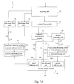
- FIG. 7A is a block diagram of an image processing circuit in accordance with a second embodiment of the present invention.
- FIG. 7B is a spectrum of an image signal in accordance with another embodiment of the present invention.
- FIG. 8 is a block diagram of an image processing circuit in accordance with a third embodiment of the present invention.
- a first part discusses a two-dimensional (2D) image processing method according to the present invention
- a second part discusses the basis of how the 2D image processing method is capable of solving the problem of formation of abnormal color blocks in a multi-burst pattern
- a third part discusses problems of the second 2D image processing method
- a fourth part discusses how to define a weight of a chromaticity
- a fifth part discusses how to define a weight of a luminosity.
- an image processing method of the prior art a single pixel is processed to calculate a chromaticity.
- an image processing method of the present invention at least three pixels successively arranged in a same vertical line are processed to calculate a chromaticity. Therefore, in the following description, the image processing method of the prior art is called a one-dimensional method, and the image processing method according to the present invention is called a 2D image processing method.
- FIG. 4 shows a block diagram of an image processing circuit 3 in accordance with a first embodiment of the present invention.
- the image processing circuit implementing the 2D image processing method according to the present invention comprises a receiving unit 30 , a vertical filter module 32 , a frequency demodulation module 34 and a chroma converting unit 36 .
- the vertical filter module 32 coupled to the receiving unit 30 filters out luma components of an image signal to retain a chroma signal.
- the frequency demodulation module 34 coupled to the vertical filter module 32 demodulates a chroma angular frequency of the chroma signal.
- the chroma converting unit 36 coupled to the frequency demodulation module 34 converts the chroma angular frequency to a chromaticity.
- the receiving unit 30 receives an image encoded according to the SECAM specification.
- the image at least comprises three pixels, which are successively arranged in a same vertical line and respectively corresponding to a first image signal S 1 , a second image signal S 2 and a third image signal S 3 .
- the vertical filter module 32 calculates a chroma signal according to the first image signal S 1 , the second image signal S 2 and the third image signal S 3 .
- the frequency demodulation module 34 calculates a chroma angular frequency according to the chroma signal, and the chroma converting unit 36 finds a first chromaticity V 1 corresponding to the chroma angular frequency.
- the vertical filter module 32 comprises a first multiplication unit 320 and an addition unit 322 .
- the first multiplication unit 320 respectively multiplies the first image signal S 1 , the second image signal S 2 and the third image signal S 3 by a first multiple, a second multiple and a third multiple. A sum of the first multiple, the second multiple and the third multiple is zero.
- the addition unit 322 coupled to the first multiplication unit 320 adds up the multiplied first image signal, the multiplied second image signal and the multiplied third image signal. Since the sum of the first multiple, the second multiple and the third multiple is zero, a sum of the luma components is zero, thus filtering a chroma signal of the image signal.
- a signal based on the SECAM system has characteristics below.
- the signal comprises three successively, vertically arranged pixels, which respectively correspond to three image signals.
- a difference ⁇ is present between a phase of one pixel and those of the other two pixels (supposing that the three pixels have the same luminosity and chromaticity).
- the first multiplication unit 320 respectively multiplies S 1 , S 2 and S 3 by the first multiple N 1 , the second multiple N 2 and the third multiple N 3 to obtain three products to be added up by the addition unit 322 , where a sum of N 1 , N 2 and N 3 is zero.
- the vertical filter module 32 filters to effectively retain the chroma signal in the image signal, and the chroma signal is called a first chroma signal in the following description.
- the first chroma signal filtered from the vertical filter module 32 is transmitted to the frequency demodulation module 34 for demodulating a first chroma angular frequency ( ⁇ ) of the first chroma signal.
- Operation principle of the frequency demodulation module 34 is identical to that of the frequency demodulation module 14 and shall not be further disclosed for brevity.
- an absolute value of ⁇ is no more than ⁇ (180 degrees), such that a difference between two phrases corresponding to two pixels lies between ⁇ to ⁇ .
- 2 ⁇ is to be subtracted from the difference greater than ⁇ , and 2 ⁇ is to be added to the difference smaller than ⁇ .
- the second part discusses how the problem of formation of abnormal color blocks in a multi-burst pattern by using the 2D image processing method is solved.
- the chroma angular frequency ⁇ representing chroma is zero and Y representing luma components varies at a predetermined frequency in the multi-burst pattern.
- the luma components oscillate at an angular frequency ⁇ c + ⁇ close to the carrier angular frequency ⁇ c , where ⁇ represents a small angular frequency difference.
- the luma components being low-frequency have frequencies much lower than the carrier angular frequency ⁇ c , in a way that a conventional filter unit 11 illustrated in FIG. 2 is capable of filtering out the luma components by filtering in conjunction with a predetermined frequency range.
- the conventional filter unit 11 illustrated in FIG. 2 becomes unable to effectively filter out the luma components. That is, the luma components oscillating at the predetermined oscillating angular frequency are mistaken for chroma components, which shall create abnormal color blocks in the black and white multi-burst pattern as illustrated in FIG. 3B .
- the vertical filter module 32 of the image processing circuit 3 applies characteristics of the SECAM system to filter luma components rather than applying the frequency filter approach. Therefore, the image processing circuit according to the present invention is capable of effectively processing oscillating luma components so that abnormal color blocks in a black and white multi-burst pattern are not formed after decoding.
- the third part discusses problems of the 2D image processing method.
- the image processing image method may generate undesirable results when implementing the image processing circuit 3 illustrated in FIG. 4 in two situations: (a) cross-chroma areas and (b) a non-uniform color distribution, both of which shall be described below.
- the situation (a) is to be discussed with reference to FIG. 5 .
- an edge of the area intercepts the three successive pixels, and thus one of the pixels has an angular oscillating frequency different from those of the other two pixels.
- the vertical filter module 32 calculates and generates an item Sin [( ⁇ c + ⁇ 1 )*t]+Sin [( ⁇ c + ⁇ 2 )*t], which is equal to signals having oscillating frequencies ⁇ c + ⁇ 1 and ⁇ c + ⁇ 2 .
- the chromaticity calculated by the frequency demodulation module 34 and the chroma converting unit 36 illustrated in FIG. 4 is a result of mixing colors corresponding to ⁇ 1 and ⁇ 2 but not colors corresponding to ⁇ 1 or ⁇ 2 . That is, in the situation (a) of cross-chroma areas, a color different from two adjacent chroma areas is decoded and a color block is formed at the edge of chroma areas as illustrated in FIG. 5 .
- FIG. 5 shows an abnormal color block 22 being formed at the edge between two adjacent chroma areas having different chromaticities.
- + ⁇ is a phase difference defined in the SECAM specification
- ⁇ 1 , ⁇ 2 and ⁇ 3 are phase differences resulting from the non-uniform color distribution at the front-end.
- phase differences of the image signals corresponding to the successively arranged pixels are not simply equal to the difference ⁇ .
- a phase difference between ⁇ 1 , ⁇ 2 and ⁇ 3 + ⁇ is zero.
- the phase difference is transmitted to the vertical filter module 32 illustrated in FIG. 4 to output a result of zero regarded as a signal represented by Sin [( ⁇ c +( ⁇ c ))*t]. That is, an absolute value of the chroma angular frequency is equal to the carrier angular frequency; however, the chroma frequency is in fact not equal to the carrier frequency.
- FIG. 6 shows horizontally adjacent chroma areas with different chromaticities, and colors of the left side are non-uniformly distributed, such that abnormal blocks 24 result at the adjoining edge of the horizontally adjacent chroma areas.
- the fourth part discusses defining a weight of a chromaticity.
- an approach of involving weights is defined. More particularly, referring to FIG. 7A , a same image is processed via a 2D image processing method (i.e., using a vertical filter module 52 , a frequency demodulation module 54 and a chroma converting unit 58 ) to obtain a first chromaticity, and via a one-dimensional image processing method (i.e., using a band-pass filter unit 51 , a frequency demodulation module 54 and a chroma converting unit 58 ) to obtain a second chromaticity.
- a 2D image processing method i.e., using a vertical filter module 52 , a frequency demodulation module 54 and a chroma converting unit 58
- a one-dimensional image processing method i.e., using a band-pass filter unit 51 , a frequency demodulation module 54 and a chroma converting unit 58
- the first chromaticity and the second chromaticity are respectively multiplied by a first weight and a second weight to calculate a representative chromaticity.
- a first weight and a second weight By adjusting the first weight and the second weight, importance of the first chromaticity and the second chromaticity is defined. Accordingly, the image processing method according to an embodiment of the present invention may be applied to different color display situations, thereby rendering better application flexibility to the image processing method according to the invention.
- an image processing circuit 5 comprises a chroma weight module 56 coupled to the chroma converting unit 58 .
- the chroma weight module 56 respectively multiplies a first chromaticity V 1 and a second chromaticity V 2 by the first weight and the second weight to calculate a representative chromaticity V 0 .
- the chroma weight module 56 comprises a first defining unit 560 , a second defining unit 562 and a third defining unit 564 .
- a chromaticity is weighted with respect to different situations, and a detailed flow thereof shall be described below.
- an angular frequency difference between a first chroma angular frequency calculated in the 2D image processing method and a carrier angular frequency based on the SECAM system may be rather large, and thus the first defining unit 560 properly reduces the first weight and increases the second weight for such situation. That is, when the angular frequency difference between the first chroma angular frequency and the carrier angular frequency based on the SECAM system is rather large, an undesirable effect may be resulted according to the 2D image processing method. Therefore, the 2D image processing method according to an embodiment of the present invention is incorporated with the one-dimensional image processing method to gain a better effect.
- the first defining unit 560 determines whether the first chroma angular frequency is greater than a predetermined threshold. When the answer is yes, the first weight is defined as being smaller than the second weight; otherwise, the first weight is defined as being greater than the second weight.
- An image received by a receiving unit 50 further comprises a fourth pixel and a fifth pixel. Further, in a vertical direction, the fourth pixel, the first pixel, the second pixel, the third pixel, and the fifth pixel, successively arranged downwards, respectively corresponds to a fourth image signal, the first image signal, the second image signal, the third image signal and a fifth image signal.
- the vertical filter module 52 , the frequency demodulation module 54 and the chroma converting unit 58 calculates a third chromaticity V 3 according to the fourth, the first and the second image signals, and calculates a fourth chromaticity V 4 according to the second, the third and the fifth image signals.
- the image processing circuit 5 further comprises a chroma edge detecting module 55 coupled to the chroma converting unit 58 .
- the chroma edge detecting module 55 calculates a chroma edge intensity (i.e., chromaticity difference) according to the third chromaticity V 3 , the first chromaticity V 1 and the fourth chromaticity V 4 , which are outputted by the chroma converting unit 58 .
- the second defining unit 562 of the chroma weight module 56 coupled to the chroma edge detecting module 55 defines the first and second weights for calculating the representative chromaticity V 0 according to the chroma edge intensity outputted by the chroma edge detecting module 55 .
- the chroma edge intensity (chromaticity difference) is used for determining whether an edge of a chroma area is present. The calculation of the chroma edge intensity is described below.
- the chroma edge detecting module 55 comprises a first subtraction unit 550 , and a first determining unit 552 coupled to the first subtraction unit 550 .
- the first subtraction unit 550 subtracts the first chromaticity V 1 from the third chromaticity V 3 to calculate a first chromaticity difference, and subtracts the first chromaticity V 1 from the fourth chromaticity V 4 to calculate a second chromaticity difference.
- the first determining unit 552 determines whether an absolute value of the first chromaticity difference is greater than that of the second chromaticity difference. When the answer is yes, the first determining unit 552 defines the chroma edge intensity as the absolute value of the first chromaticity difference. When the answer is no, the first determining unit 552 defines the chroma edge intensity as the absolute value of the second chromaticity difference.
- the second defining unit 562 identifies whether the pixels are located at a cross-chroma area according to the chroma edge intensity. Accordingly, the second defining unit 562 defines the first weight and the second weight according to the chroma edge intensity (chromaticity difference). For example, when the chroma edge intensity is the absolute value of the first chromaticity difference and is greater than a predetermined threshold, it is rather possible that a chroma area edge exists between the first pixel and the third pixel. Therefore, the first chromaticity V 1 calculated according to the 2D image processing method is given a lower weight.
- a luma edge is also taken into consideration according to the present invention.
- the image processing circuit 5 further comprises a first notch filter unit 53 coupled to the receiving unit 50 , and a luma edge detecting module 57 coupled to the first notch filter unit 53 .
- the first notch filter unit 53 processes the first image signal, the second image signal and the third image signal to calculate a first luminosity Y 1 corresponding to the first pixel, a second luminosity Y 2 corresponding to the second pixel, and a third luminosity Y 3 corresponding to the third pixel.
- a curve 62 and a curve 64 respectively represent luma components and chroma components of image signals
- a dashed line 66 indicates that the first notch filter unit 53 retains most of low frequency signals (i.e., the luma components) and filters outs signals within a frequency range whose center is a carrier angular frequency ⁇ c (i.e., the chroma components).
- the luma edge detecting module 57 calculates a luma edge intensity according to the first luminosity Y 1 , the second luminosity Y 2 and the third luminosity Y 3 , which are outputted by the first notch filter unit 53 .
- the chroma weight module 56 comprising the third defining unit 564 is coupled to the luma edge detecting module 57 .
- the third defining unit 564 defines the first and second weights for calculating the representative chromaticity V 0 .
- the luma edge detecting module 57 calculates the luma edge intensity via a second subtraction unit 570 and a second determining unit 572 coupled to the second subtraction unit 570 .
- the second subtraction unit 570 subtracts the second luminosity Y 2 from the first luminosity Y 1 to calculate a first luminosity difference, and subtracts the second luminosity Y 2 from the third luminosity Y 3 to calculate a second luminosity difference.
- the second determining unit 572 determines whether an absolute value of the first luminosity difference is greater than that of the second luminosity difference. When the answer is yes, the second determining unit 572 defines the luma edge intensity as the absolute value of the first luminosity difference. When the answer is no, the second determining unit 572 defines the luma edge intensity as the absolute value of the second luminosity difference.
- the third defining unit 564 identifies whether a cross-luma area is present according to the luma edge intensity. For example, when the luma edge intensity is the absolute value of the first luminosity difference and is greater than a predetermined threshold, it is rather possible that a luma area edge exists between the first pixel and the third pixel. Therefore, the first chromaticity V 1 calculated according to the 2D image processing method is given a lower weight.
- the fifth part discusses how to define a weight of a luminosity. Reference may also be made to the above-mentioned description of calculating a chromaticity and defining a weight of a chromaticity. With respect to a notch filtering process for filtering luma components, a similar weight conception may be used for defining a filtering frequency range.
- the image processing circuit 7 comprises a second notch filter unit 75 , a third notch filter unit 77 and a luma weight module 76 .
- the second notch filter unit 75 and the third notch filter unit 77 are coupled to a receiving unit 70
- the luma weight module 76 is coupled to the second notch filter unit 75 and the third notch filter unit 77 .
- the receiving unit 70 receives an image based on the SECAM specification.
- the image comprises a plurality of pixels at least comprising vertically, successively arranged a first pixel, a second pixel and a third pixel respectively corresponding to a first image signal, a second image signal and a third image signal.
- the second notch filter unit 75 and the third notch filter unit 77 regard one image signal from the first, the second and the third image signals as a target image signal, and process the target image signal respectively by using a first frequency range and a second frequency range, so as to respectively calculate a fourth luminosity Y 4 and a fifth luminosity Y 5 , where the second frequency range covers the first frequency range and is greater than the first frequency range.
- the luma weight module 76 adds up two products of multiplying the fourth luminosity Y 4 by a third weight and multiplying the fifth luminosity Y 5 by a fourth weight to calculate a representative luminosity Y 0 corresponding to the target image signal.
- the luma weight module 76 obtains chromaticities via a one-dimensional image processing method and a 2D image processing method to define the third and fourth weights, and a detailed process flow thereof shall be described below.
- the image processing circuit 7 further comprises a chroma converting unit 79 , and a third subtraction unit 78 coupled to the chroma converting unit 79 .
- the third subtraction unit 78 subtracts the second chromaticity V 2 from the first chromaticity V 1 outputted by the chroma converting unit 79 to calculate a chromaticity difference.
- the luma weight module 76 comprising a fourth defining unit 760 and being coupled to the third subtraction unit 78 , defines the third weight and the fourth weight according to an absolute value of the chromaticity difference outputted by the third subtraction unit 78 .
- a narrower frequency range is applied so that the third weight is defined as being greater than the fourth weight; for smaller absolute values of the chromaticity difference, a wider frequency range is applied so that the third weight is defined as being smaller than the fourth weight.
- abnormal color blocks formed in a multi-burst pattern from applying a one-dimensional image processing method (corresponding to the image processing circuit 1 illustrated in FIG. 2 ) of the prior art, are avoided via a vertical filter calculation using a 2D image processing method (corresponding to the image processing circuit 3 illustrated in FIG. 3 ) according to an embodiment of the present invention.
- an image processing circuit such as the image processing circuit 5 illustrated in FIG. 7A properly gives a weight proportion to a first chromaticity and a second chromaticity, which are respectively calculated via the 2D image processing method according to an embodiment of the present invention and a conventional one-dimensional image method. Therefore, for different color distribution situations, a reliable chromaticity is generated according to the present invention.
- an image processing circuit such as the image processing circuit 7 illustrated in FIG. 8 determines a current color distribution according to a difference of a first chromaticity and a second chromaticity, so as to properly define a filtering frequency range for filtering luma components in a notch filtering process. Therefore, in situations of different color distributions, an image processing circuit according to an embodiment of the present invention is capable of effectively separating chroma and luma components.
Abstract
Description
S 1 =Y+Sin [(ωc+Δω)*t+φ 1],
S 2 =Y+Sin [(ωc+Δω)*t+φ 1],
S 3 =Y+Sin [(ωc+Δω)*t+φ 1+π].
N 1 *S 1 +N 2 *S 2 +N 3 *S 3 =Y*(N 1 +N 2 +N 3)+N 1*Sin [(ωc+Δω)*t+φ 1 ]+N 2*Sin [(ωc+Δω)*t+φ 1 ]+N 3*Sin [(ωc+Δω)t+φ 1 +π]=Y(N 1 +N 2 +N 3)+(N 1 +N 2 −N 3)Sin [(ωc+Δω)*t+φ 1],
S′=Y+Sin [(ωc)*t],
S 1 ′=Y+Sin [(ωc+Δω1)*t+φ 1],
S 2 ′=Y+Sin [(ωc+Δω1)*t+φ 1],
S 3 ′=Y+Sin [(ωc+Δω2)*t+φ 1+π],
where Δω2 is not equal to Δω1.
S 1 ″=Y+Sin [(ωc+Δω)*t+φ 1],
S 2 ″=Y+Sin [(ωc+Δω)*t+φ 2],
S 3 ″=Y+Sin [(ωc+Δω)*t+φ 3+π],
Claims (20)
Applications Claiming Priority (3)
| Application Number | Priority Date | Filing Date | Title |
|---|---|---|---|
| TW098102071 | 2009-01-20 | ||
| TW098102071A TWI369908B (en) | 2009-01-20 | 2009-01-20 | Image processing circuit and image processing method |
| TW98102071A | 2009-01-20 |
Publications (2)
| Publication Number | Publication Date |
|---|---|
| US20100182449A1 US20100182449A1 (en) | 2010-07-22 |
| US8421924B2 true US8421924B2 (en) | 2013-04-16 |
Family
ID=42336659
Family Applications (1)
| Application Number | Title | Priority Date | Filing Date |
|---|---|---|---|
| US12/685,384 Active 2031-08-26 US8421924B2 (en) | 2009-01-20 | 2010-01-11 | Image processing circuit and image processing method |
Country Status (2)
| Country | Link |
|---|---|
| US (1) | US8421924B2 (en) |
| TW (1) | TWI369908B (en) |
Families Citing this family (3)
| Publication number | Priority date | Publication date | Assignee | Title |
|---|---|---|---|---|
| US8212923B2 (en) * | 2010-04-13 | 2012-07-03 | Newport Media, Inc. | SECAM line identification and PAL switch |
| KR102636465B1 (en) * | 2016-10-24 | 2024-02-14 | 삼성전자주식회사 | Image processing apparatus, image processing method and electronic device |
| CN113035126B (en) * | 2021-03-10 | 2022-08-02 | 京东方科技集团股份有限公司 | Pixel rendering method and system, readable storage medium and display panel |
Citations (10)
| Publication number | Priority date | Publication date | Assignee | Title |
|---|---|---|---|---|
| US4072983A (en) * | 1976-02-24 | 1978-02-07 | Rca Corporation | SECAM identification circuit |
| US4574301A (en) * | 1983-08-24 | 1986-03-04 | U.S. Philips Corporation | SECAM Color identifying circuit |
| US5907368A (en) * | 1996-02-29 | 1999-05-25 | Fujitsu Ltd | Information processing apparatus having function capable of displaying image by television signal |
| US6377313B1 (en) * | 1999-09-02 | 2002-04-23 | Techwell, Inc. | Sharpness enhancement circuit for video signals |
| US20030210829A1 (en) * | 2002-03-08 | 2003-11-13 | Ikuo Someya | Image processing apparatus |
| US20050134731A1 (en) * | 2003-11-24 | 2005-06-23 | Samsung Electronics Co., Ltd. | Method of converting resolution of video signals and apparatus using the same |
| US20050174444A1 (en) * | 2002-09-11 | 2005-08-11 | Akira Ueno | Electronic camera apparatus and image processing method thereof |
| US7023487B1 (en) * | 2002-01-25 | 2006-04-04 | Silicon Image, Inc. | Deinterlacing of video sources via image feature edge detection |
| US7535514B2 (en) * | 2004-10-25 | 2009-05-19 | Samung Electronics Co., Ltd. | Apparatus and method for decoding SECAM chrominance signal |
| US8009872B2 (en) * | 2006-02-01 | 2011-08-30 | Sony Corporation | Taken-image signal-distortion compensation method, taken-image signal-distortion compensation apparatus, image taking method and image-taking apparatus |
-
2009
- 2009-01-20 TW TW098102071A patent/TWI369908B/en not_active IP Right Cessation
-
2010
- 2010-01-11 US US12/685,384 patent/US8421924B2/en active Active
Patent Citations (10)
| Publication number | Priority date | Publication date | Assignee | Title |
|---|---|---|---|---|
| US4072983A (en) * | 1976-02-24 | 1978-02-07 | Rca Corporation | SECAM identification circuit |
| US4574301A (en) * | 1983-08-24 | 1986-03-04 | U.S. Philips Corporation | SECAM Color identifying circuit |
| US5907368A (en) * | 1996-02-29 | 1999-05-25 | Fujitsu Ltd | Information processing apparatus having function capable of displaying image by television signal |
| US6377313B1 (en) * | 1999-09-02 | 2002-04-23 | Techwell, Inc. | Sharpness enhancement circuit for video signals |
| US7023487B1 (en) * | 2002-01-25 | 2006-04-04 | Silicon Image, Inc. | Deinterlacing of video sources via image feature edge detection |
| US20030210829A1 (en) * | 2002-03-08 | 2003-11-13 | Ikuo Someya | Image processing apparatus |
| US20050174444A1 (en) * | 2002-09-11 | 2005-08-11 | Akira Ueno | Electronic camera apparatus and image processing method thereof |
| US20050134731A1 (en) * | 2003-11-24 | 2005-06-23 | Samsung Electronics Co., Ltd. | Method of converting resolution of video signals and apparatus using the same |
| US7535514B2 (en) * | 2004-10-25 | 2009-05-19 | Samung Electronics Co., Ltd. | Apparatus and method for decoding SECAM chrominance signal |
| US8009872B2 (en) * | 2006-02-01 | 2011-08-30 | Sony Corporation | Taken-image signal-distortion compensation method, taken-image signal-distortion compensation apparatus, image taking method and image-taking apparatus |
Also Published As
| Publication number | Publication date |
|---|---|
| US20100182449A1 (en) | 2010-07-22 |
| TW201029476A (en) | 2010-08-01 |
| TWI369908B (en) | 2012-08-01 |
Similar Documents
| Publication | Publication Date | Title |
|---|---|---|
| US7227990B2 (en) | Color image processing device and color image processing method | |
| US5325186A (en) | Motion adaptive luminance signal and color signal separating filter | |
| KR20060065478A (en) | Sub-carrier detection (scd) for motion threshold logic | |
| US4716462A (en) | Motion adaptive television signal processing system | |
| US8421924B2 (en) | Image processing circuit and image processing method | |
| KR101358409B1 (en) | Signal processing apparatus and control method thereof | |
| US20060268179A1 (en) | Motion detector for a video display system | |
| US5208662A (en) | Method of encoding color television signal and a circuit therefor | |
| US5715015A (en) | Method of enhancing details contained in a color signal and a circuit for implementing the same in a color video apparatus | |
| US20100303376A1 (en) | Circuit and method for processing image | |
| US7724308B2 (en) | Cross color suppressing apparatus and method thereof | |
| US5150203A (en) | Variable chrominance filtering for encoding television signals | |
| JP2003348379A (en) | Image display device and image processing apparatus, and image processing method | |
| CN1179576C (en) | Color transmission system discrimination circuit in television set | |
| JPH0530526A (en) | Color edge correcting circuit | |
| US20040179141A1 (en) | Method, apparatus, and system for reducing cross-color distortion in a composite video signal decoder | |
| KR100306756B1 (en) | Method for Enhancing the Edge of Color Image Based on Luminance Component | |
| JPH07111605A (en) | Noise elimination circuit | |
| JP3351630B2 (en) | Y / C separation circuit | |
| JP3555744B2 (en) | Contour correction device | |
| KR100408032B1 (en) | Filter for eliminating a dot pattern and method thereof | |
| CN101808249B (en) | Image processing circuit and image processing method | |
| JP3600678B2 (en) | Television signal processing method and television signal processing device | |
| US7310119B1 (en) | Adaptive circuit for Y-C separation | |
| US8718395B2 (en) | Image processing apparatus, display apparatus provided with same, and image processing method |
Legal Events
| Date | Code | Title | Description |
|---|---|---|---|
| AS | Assignment |
Owner name: MSTAR SEMICONDUCTOR, INC., TAIWAN Free format text: ASSIGNMENT OF ASSIGNORS INTEREST;ASSIGNOR:LIAO, MING-HAO;REEL/FRAME:023763/0436 Effective date: 20091230 |
|
| STCF | Information on status: patent grant |
Free format text: PATENTED CASE |
|
| FPAY | Fee payment |
Year of fee payment: 4 |
|
| AS | Assignment |
Owner name: MEDIATEK INC., TAIWAN Free format text: MERGER;ASSIGNOR:MSTAR SEMICONDUCTOR, INC.;REEL/FRAME:052931/0468 Effective date: 20190115 |
|
| MAFP | Maintenance fee payment |
Free format text: PAYMENT OF MAINTENANCE FEE, 8TH YEAR, LARGE ENTITY (ORIGINAL EVENT CODE: M1552); ENTITY STATUS OF PATENT OWNER: LARGE ENTITY Year of fee payment: 8 |