US8404591B2 - Method of fabricating complementary metal-oxide-semiconductor (CMOS) device - Google Patents
Method of fabricating complementary metal-oxide-semiconductor (CMOS) device Download PDFInfo
- Publication number
- US8404591B2 US8404591B2 US13/482,044 US201213482044A US8404591B2 US 8404591 B2 US8404591 B2 US 8404591B2 US 201213482044 A US201213482044 A US 201213482044A US 8404591 B2 US8404591 B2 US 8404591B2
- Authority
- US
- United States
- Prior art keywords
- layer
- etching solution
- dielectric layer
- etching
- substrate
- Prior art date
- Legal status (The legal status is an assumption and is not a legal conclusion. Google has not performed a legal analysis and makes no representation as to the accuracy of the status listed.)
- Active
Links
Images


Classifications
-
- H—ELECTRICITY
- H10—SEMICONDUCTOR DEVICES; ELECTRIC SOLID-STATE DEVICES NOT OTHERWISE PROVIDED FOR
- H10D—INORGANIC ELECTRIC SEMICONDUCTOR DEVICES
- H10D64/00—Electrodes of devices having potential barriers
- H10D64/60—Electrodes characterised by their materials
- H10D64/66—Electrodes having a conductor capacitively coupled to a semiconductor by an insulator, e.g. MIS electrodes
- H10D64/68—Electrodes having a conductor capacitively coupled to a semiconductor by an insulator, e.g. MIS electrodes characterised by the insulator, e.g. by the gate insulator
- H10D64/691—Electrodes having a conductor capacitively coupled to a semiconductor by an insulator, e.g. MIS electrodes characterised by the insulator, e.g. by the gate insulator comprising metallic compounds, e.g. metal oxides or metal silicates
-
- H—ELECTRICITY
- H10—SEMICONDUCTOR DEVICES; ELECTRIC SOLID-STATE DEVICES NOT OTHERWISE PROVIDED FOR
- H10D—INORGANIC ELECTRIC SEMICONDUCTOR DEVICES
- H10D64/00—Electrodes of devices having potential barriers
- H10D64/60—Electrodes characterised by their materials
- H10D64/66—Electrodes having a conductor capacitively coupled to a semiconductor by an insulator, e.g. MIS electrodes
- H10D64/667—Electrodes having a conductor capacitively coupled to a semiconductor by an insulator, e.g. MIS electrodes the conductor comprising a layer of alloy material, compound material or organic material contacting the insulator, e.g. TiN workfunction layers
-
- H—ELECTRICITY
- H10—SEMICONDUCTOR DEVICES; ELECTRIC SOLID-STATE DEVICES NOT OTHERWISE PROVIDED FOR
- H10D—INORGANIC ELECTRIC SEMICONDUCTOR DEVICES
- H10D64/00—Electrodes of devices having potential barriers
- H10D64/60—Electrodes characterised by their materials
- H10D64/66—Electrodes having a conductor capacitively coupled to a semiconductor by an insulator, e.g. MIS electrodes
- H10D64/68—Electrodes having a conductor capacitively coupled to a semiconductor by an insulator, e.g. MIS electrodes characterised by the insulator, e.g. by the gate insulator
- H10D64/681—Electrodes having a conductor capacitively coupled to a semiconductor by an insulator, e.g. MIS electrodes characterised by the insulator, e.g. by the gate insulator having a compositional variation, e.g. multilayered
- H10D64/685—Electrodes having a conductor capacitively coupled to a semiconductor by an insulator, e.g. MIS electrodes characterised by the insulator, e.g. by the gate insulator having a compositional variation, e.g. multilayered being perpendicular to the channel plane
-
- H—ELECTRICITY
- H10—SEMICONDUCTOR DEVICES; ELECTRIC SOLID-STATE DEVICES NOT OTHERWISE PROVIDED FOR
- H10D—INORGANIC ELECTRIC SEMICONDUCTOR DEVICES
- H10D84/00—Integrated devices formed in or on semiconductor substrates that comprise only semiconducting layers, e.g. on Si wafers or on GaAs-on-Si wafers
- H10D84/01—Manufacture or treatment
- H10D84/0123—Integrating together multiple components covered by H10D12/00 or H10D30/00, e.g. integrating multiple IGBTs
- H10D84/0126—Integrating together multiple components covered by H10D12/00 or H10D30/00, e.g. integrating multiple IGBTs the components including insulated gates, e.g. IGFETs
- H10D84/0165—Integrating together multiple components covered by H10D12/00 or H10D30/00, e.g. integrating multiple IGBTs the components including insulated gates, e.g. IGFETs the components including complementary IGFETs, e.g. CMOS devices
- H10D84/0172—Manufacturing their gate conductors
- H10D84/0177—Manufacturing their gate conductors the gate conductors having different materials or different implants
-
- H—ELECTRICITY
- H10—SEMICONDUCTOR DEVICES; ELECTRIC SOLID-STATE DEVICES NOT OTHERWISE PROVIDED FOR
- H10D—INORGANIC ELECTRIC SEMICONDUCTOR DEVICES
- H10D84/00—Integrated devices formed in or on semiconductor substrates that comprise only semiconducting layers, e.g. on Si wafers or on GaAs-on-Si wafers
- H10D84/01—Manufacture or treatment
- H10D84/0123—Integrating together multiple components covered by H10D12/00 or H10D30/00, e.g. integrating multiple IGBTs
- H10D84/0126—Integrating together multiple components covered by H10D12/00 or H10D30/00, e.g. integrating multiple IGBTs the components including insulated gates, e.g. IGFETs
- H10D84/0165—Integrating together multiple components covered by H10D12/00 or H10D30/00, e.g. integrating multiple IGBTs the components including insulated gates, e.g. IGFETs the components including complementary IGFETs, e.g. CMOS devices
- H10D84/0181—Manufacturing their gate insulating layers
-
- H—ELECTRICITY
- H10—SEMICONDUCTOR DEVICES; ELECTRIC SOLID-STATE DEVICES NOT OTHERWISE PROVIDED FOR
- H10D—INORGANIC ELECTRIC SEMICONDUCTOR DEVICES
- H10D84/00—Integrated devices formed in or on semiconductor substrates that comprise only semiconducting layers, e.g. on Si wafers or on GaAs-on-Si wafers
- H10D84/01—Manufacture or treatment
- H10D84/0123—Integrating together multiple components covered by H10D12/00 or H10D30/00, e.g. integrating multiple IGBTs
- H10D84/0126—Integrating together multiple components covered by H10D12/00 or H10D30/00, e.g. integrating multiple IGBTs the components including insulated gates, e.g. IGFETs
- H10D84/0165—Integrating together multiple components covered by H10D12/00 or H10D30/00, e.g. integrating multiple IGBTs the components including insulated gates, e.g. IGFETs the components including complementary IGFETs, e.g. CMOS devices
- H10D84/0188—Manufacturing their isolation regions
-
- H—ELECTRICITY
- H10—SEMICONDUCTOR DEVICES; ELECTRIC SOLID-STATE DEVICES NOT OTHERWISE PROVIDED FOR
- H10D—INORGANIC ELECTRIC SEMICONDUCTOR DEVICES
- H10D84/00—Integrated devices formed in or on semiconductor substrates that comprise only semiconducting layers, e.g. on Si wafers or on GaAs-on-Si wafers
- H10D84/01—Manufacture or treatment
- H10D84/02—Manufacture or treatment characterised by using material-based technologies
- H10D84/03—Manufacture or treatment characterised by using material-based technologies using Group IV technology, e.g. silicon technology or silicon-carbide [SiC] technology
- H10D84/038—Manufacture or treatment characterised by using material-based technologies using Group IV technology, e.g. silicon technology or silicon-carbide [SiC] technology using silicon technology, e.g. SiGe
-
- H—ELECTRICITY
- H10—SEMICONDUCTOR DEVICES; ELECTRIC SOLID-STATE DEVICES NOT OTHERWISE PROVIDED FOR
- H10P—GENERIC PROCESSES OR APPARATUS FOR THE MANUFACTURE OR TREATMENT OF DEVICES COVERED BY CLASS H10
- H10P50/00—Etching of wafers, substrates or parts of devices
- H10P50/20—Dry etching; Plasma etching; Reactive-ion etching
- H10P50/28—Dry etching; Plasma etching; Reactive-ion etching of insulating materials
- H10P50/282—Dry etching; Plasma etching; Reactive-ion etching of insulating materials of inorganic materials
- H10P50/283—Dry etching; Plasma etching; Reactive-ion etching of insulating materials of inorganic materials by chemical means
Definitions
- the present invention generally relates to methods of fabricating complementary metal-oxide-semiconductor (CMOS) devices, and more particularly to a method of fabricating a CMOS device having high dielectric constant (high-k) dielectric layer and metal gate electrode.
- CMOS complementary metal-oxide-semiconductor
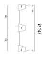
- FIGS. 1A-1E are schematic sectional views illustrating a conventional method of fabricating a CMOS device including high-k dielectric layer and metal gate electrode.
- a semiconductor substrate 100 having a plurality of shallow trench isolation (STI) structures 102 formed therein defining an N-type MOS region 104 and a P-type MOS region 106 is provided.
- a silicon oxide layer 108 and a hafnium oxide (HfO2) layer 110 are sequentially formed over the substrate 100 .
- the hafnium oxide layer 110 is comprised of a high-k dielectric material layer, the silicon oxide layer 108 serves as an interfacial layer (IL) between the substrate 100 and the hafnium oxide layer 110 .
- a lanthanum oxide (LaO) layer 112 and an aluminum oxide (AlO) layer 114 are respectively formed over a portion of the hafnium oxide layer 110 at the N-type MOS region 104 and another portion of the hafnium oxide layer 110 at the P-type MOS region 106 , for adjusting work functions of respective metal gate electrode.
- LaO lanthanum oxide
- AlO aluminum oxide
- multiple gate stacked structures 116 are formed over the substrate 100 and respectively cover a part of the lanthanum oxide layer 112 and a part of the aluminum oxide layer 114 .
- Each of the gate stacked structures 116 is comprised of a titanium nitride layer 118 , a poly-silicon layer 120 and a hard mask layer 122 in an order from bottom to top.
- a wet etching step 124 is performed; so that portions of the aluminum oxide layer 114 and the lanthanum oxide layer 112 uncovered by the gate stacked structures 116 are removed and thereby formed a patterned aluminum oxide layer 114 a and a patterned lanthanum oxide layer 112 a.
- the wet etching step 124 sequentially includes: loading the CMOS device into an etching machine, using a diluted hydrochloric acid (HCl) as etching solution, etching both the aluminum oxide layer 114 and the lanthanum oxide layer 112 , cleaning device surfaces by using distilled water to remove residual etching solution, blow drying the device, and removing the device out from the etching machine.
- HCl diluted hydrochloric acid
- the wet etching step 126 sequentially includes: loading the CMOS device into the etching machine, using a diluted hydrofluoric acid (HF) as etching solution, etching the hafnium oxide layer 110 and the silicon oxide layer 108 , cleaning device surfaces by using a distilled water to remove residual etching solution, blow drying the device, and removing the device out from the etching machine.
- HF diluted hydrofluoric acid
- the polymers or other residues adhere on to the surface of the device, which would adversely influence the subsequent fabrication process and lead to poor yield and degrade the device performance.
- the present invention relates to a method for fabricating a CMOS device that may reduce the possibility of polymers or other residues from adhering to the surface of the device to cause degrade the device performance and poor yield.
- a method of fabricating a CMOS device in accordance with an embodiment is provided. First, an isolation structure is formed in a substrate to define a first-type MOS region and a second-type MOS region. Next, an interfacial layer and a high-k dielectric layer are sequentially formed on the substrate. Next, a first cover layer and a second cover layer are respectively over a portion of the high-k dielectric layer at the first-type MOS region and another portion of the high-k dielectric layer at the second-type MOS region.
- a first gate stacked structure and a second gate stacked structure respectively are formed over a part of the first cover layer and a part of the second cover layer, wherein the first gate stacked structure and the second gate stacked structure include, in a bottom-to-top-order, a first conductive layer, a second conductive layer and a hard mask layer.
- an in-situ wet etching step is performed using a first etching solution to etch the first and second cover layers and a second etching solution to etch both the high-k dielectric layer and the interfacial layer until the substrate is exposed, wherein the second etching solution is a mixed etching solution containing the first etching solution.
- the high-k dielectric layer is, for example, a hafnium-containing dielectric layer.
- the high-k dielectric layer is, for example, a hafnium oxide layer.
- the first cover layer and the second cover layer are, for example high-k material layers.
- the first-type MOS region is an N-type MOS region
- the second-type MOS region is a P-type MOS region
- the first cover layer is, for example a lanthanum oxide layer
- the second cover layer is, for example an aluminum oxide layer.
- the first etching solution is a diluted hydrochloric acid
- the second etching solution is a mixed etching solution containing a diluted hydrochloric acid and a diluted hydrofluoric acid.
- a third etching solution is used after using the second etching solution; whose composition is the same as the first etching solution.
- the first conductive layer is, for example a metal layer.
- a material of the first conductive layer is one selected from the group consisting of tungsten, aluminum, aluminum copper alloys, copper, titanium, titanium silicide, cobalt, cobalt silicide, nickel, nickel silicide, titanium nitride, titanium tungsten alloys and tantalum nitride.
- the second conductive layer is, for example a poly-silicon layer.
- the interfacial layer is, for example a silicon oxide layer.
- the method further includes performing a plasma treatment step before performing the in-situ wet etching step.
- a gas used in the plasma treatment step includes argon and/or boron trichloride.
- the present method employs the in-situ method and performs the wet etching step to the dielectric layer without removing the device out of the etching machine, and therefore it not only can be readily integrated with general CMOS fabrication process, but also can make the fabrication process much more simple and convenient.
- the method may directly replace the etching solution and then use the mixed etching solution to etch the dielectric layer in the same etching machine, and therefore it may not only increase the etching efficiency and avoid polymers or other residues from adhering to device surfaces, but also may improve the subsequent manufacturing process and the issues associated with the degradation of device performance and yield.
- a plasma treatment step to a device surface can be performed for facilitating the subsequent wet etching step.
- FIGS. 1A-1E are schematic sectional views illustrating a conventional method of fabricating a CMOS device having high-k dielectric layer and metal gate electrode.
- FIGS. 2A-2E are schematic sectional views illustrating a method of fabricating a CMOS device having high-k dielectric layer and metal gate electrode, in accordance with an embodiment of the present invention.
- FIG. 3 is a schematic flow chart of an in-situ wet etching step in accordance with an embodiment of the present invention.
- FIGS. 4A and 4B are scanning electron microscope (SEM) images of a device manufactured by a method in accordance with the embodiment of the present invention.
- FIGS. 2A-2E are schematic sectional views illustrating a method of fabricating a CMOS device having high-k dielectric layer and metal gate electrode, in accordance with an embodiment of the present invention.
- a substrate 200 for example, a semiconductor substrate.
- Multiple isolation structures 202 are formed in the substrate 200 to define a first-type MOS region 204 and a second-type MOS region 206 .
- the isolation structures 202 are, for example, shallow trench isolation (STI) structures.
- the first-type MOS region 204 is, for example, an N-type MOS region
- the second-type MOS region 206 is, for example, a P-type MOS region.
- an interfacial layer (IL) 208 is formed over the substrate 200 .
- the interfacial layer 208 is, for example, a silicon oxide layer.
- the process for forming the interfacial layer 208 includes, for example, a chemical vapor deposition process; a plasma enhanced chemical vapor deposition process or rapid thermal process.
- a high-k dielectric layer 210 is formed over the interfacial layer 208 .
- the high-k dielectric layer 210 comprises, for example, a hafnium-containing dielectric layer.
- the high-k dielectric layer 210 includes, for example, a hafnium oxide layer.
- the process for forming the high-k dielectric layer 210 includes, for example, a deposition process or a sputtering process.
- the interfacial layer 208 may be used for promoting adhesion between the high-k dielectric layer 210 and the substrate 200 .
- a first cover layer 212 and a second cover layer 214 are respectively formed over a portion of the high-k dielectric layer 210 at the first-type MOS region 204 and another portion of the high-k dielectric layer 210 at the second-type MOS region 206 .
- the first cover layer 212 and the second cover layer 214 are used for adjusting work functions of respective metal gate electrodes.
- the first cover layer 212 and the second cover layer 214 are for example high-k material layers.
- the first cover layer 212 includes, for example, a lanthanum oxide (LaO) layer
- the second cover layer 214 includes, for example, an aluminum oxide (AlO) layer.
- the process for forming the first cover layer 212 and the second cover layer 214 includes, for example: first depositing a first cover material layer (not shown) covering the entire high-k dielectric layer 210 , forming a masking layer (not shown) over the portion of the first cover material layer at the first-type MOS region 204 , etching the first cover material layer using the masking layer as etching mask to form the first cover layer 212 , and removing the masking layer at the first-type MOS region 204 ; depositing a second cover material layer (not shown) to cover the portion of the high-k dielectric layer 210 at the second-type MOS region 206 and the first cover layer 212 , forming a masking layer (not shown) on a portion of the second cover material layer at the second-type MOS region 206 , etching the second cover material layer using the masking layer as etching mask to form the second cover layer 214 , and removing the masking layer at the second-type MOS region 206 .
- a first gate stacked structure 215 and a second gate stacked structure 216 are respectively formed on a part of the first cover layer 212 and a part of the second cover layer 214 .
- the first gate stacked structure 215 and the second gate stacked structure 216 each are comprised of, in an order from bottom-to-top from the substrate 200 , a first conductive layer 218 , a second conductive layer 220 and a hard mask layer 222 .
- the first conductive layer 218 includes, for example a metal layer, and a material of the metal layer includes, for example, one selected from the group consisting of tungsten, aluminum, aluminum copper alloys, copper, titanium, titanium silicide, cobalt, cobalt silicide, nickel, nickel silicide, titanium nitride, titanium tungsten alloys and tantalum nitride.
- the first conductive layer 218 includes, for example, a titanium nitride layer.
- the second conductive layer 220 includes, for example a poly-silicon layer.
- the hard mask layer 222 includes, for example a silicon nitride layer.
- the process for forming the first gate stacked structure 215 and the second gate stacked structure 216 includes, for example: sequentially depositing a first conductive material layer (not shown), a second conductive material layer (not shown) and a hard mask material layer (not shown) over the first cover layer 212 and the second cover layer 214 , forming a patterned photo-resist layer (not shown) over the hard mask material layer, etching the hard mask material layer using the patterned photo-resist layer as etching mask to form the hard mask layer 222 , removing the patterned photo-resist layer, etching the second conductive material layer and the first conductive material layer using the hard mask layer 222 as etching mask to form the second conductive layer 220 and the first conductive layer 218 .
- the first gate stacked structure 215 and the second gate stacked structure 216 over the first-type MOS region 204 and the second-type MOS region 206 are respectively formed.
- FIG. 3 is a flow chart of an in-situ wet etching step according to an embodiment.
- a wet etching step 225 is performed.
- the first cover layer 212 and the second cover layer 214 are first etched; the high-k dielectric layer 210 and the interfacial layer 208 are etched then until the substrate 200 is exposed such that the device is not removed out of the etching machine.
- a first cover layer 212 a , a second cover layer 214 a , high-k dielectric layers 210 a and interfacial layers 108 a are formed as the gate dielectric layers.
- the wet etching step 225 includes: in the same etching machine, at step 310 , a first etching solution is used to remove the portions of the first cover layer 212 and the second cover layer 214 respectively not covered by the first gate stacked structure 215 and the second gate stacked structure 216 .
- the device surfaces is cleaned by using a distilled water to remove residual etching solution.
- a second etching solution is used to remove exposed portions of both the high-k dielectric layer 210 and the interfacial layer 208 .
- the device surfaces are cleaned by using a distilled water to remove residual etching solution.
- the device is blow dried.
- the device is removed out of the etching machine to complete the etching step.
- the first etching solution includes, for example, a diluted hydrochloric acid;
- the second etching solution includes a mixed etching solution containing the first etching solution, for example, the second etching solution includes a mixture of a diluted hydrochloric acid and a diluted hydrofluoric acid.
- unused portions of the dielectric layers can be completely removed by using a mixed etching solution in-situ, therefore the issues associated with the subsequent fabrication process causing degradation of device performance and poor yield due to the polymers or other residues adhering to the device surfaces as described in the prior art may be effectively avoided.
- the fabrication process may be simplified and can also be easily integrated into the general CMOS device fabrication process.
- SEM scanning electron microscope
- a third etching solution may be applied on the device without removing it out of the etching machine, so as to further clean or increase the etching efficiency of the dielectric layers of the device and reduce the possible adhesion of the polymers or other residues.
- the third etching solution may be the same as the first etching solution, and may be comprised of, for example, a diluted hydrochloric acid. That is, as illustrated in FIG.
- the third etching solution may be applied (as illustrated by the reference 360 ) and then a distilled water may be used to perform a cleaning step (as illustrated by the reference 370 ).
- a plasma treatment step 227 may be performed so as to promote the performance of the subsequent etching step.
- the plasma treatment step 227 may include, for example, an argon (Ar) gas source to make the structures of the first cover layer 212 and the second cover layer 214 relatively loose and thereby increase the etching velocity for the high-k dielectric layer 210 .
- the plasma treatment step 227 may include, for example, boron chloride (BCl3) gas source. Additionally, the plasma treatment step 227 may include, for example, an argon and boron trichloride gas source.
- the method of fabricating a CMOS device includes an in-situ wet etching step such that the wet etching step is performed within the etching machine without removing the device out of the etching machine to replace the conventional two wet etching steps for etching of the dielectric layers (i.e., the cover layers, the high-k dielectric layer and interfacial layer).
- the method of the present invention may not only be integrated into the general CMOS device fabrication process, but also may make the fabrication process relatively simple and convenient.
- the method of the present invention may directly replace the etching solution after etching the cover layers and use the mixed etching solution to etch both the high-k dielectric layer and the interfacial layer in the same etching machine, which would not only increase the etching efficiency and avoid polymers or other residues adhering to the device surfaces, but also may improve the subsequent fabrication process and reduce the possible degradation of device performance and yield.
- a plasma treatment step may be applied to a device surface, which may promote the subsequent etching step.
Landscapes
- Metal-Oxide And Bipolar Metal-Oxide Semiconductor Integrated Circuits (AREA)
- Insulated Gate Type Field-Effect Transistor (AREA)
Abstract
Description
Claims (20)
Priority Applications (1)
| Application Number | Priority Date | Filing Date | Title |
|---|---|---|---|
| US13/482,044 US8404591B2 (en) | 2010-09-02 | 2012-05-29 | Method of fabricating complementary metal-oxide-semiconductor (CMOS) device |
Applications Claiming Priority (2)
| Application Number | Priority Date | Filing Date | Title |
|---|---|---|---|
| US12/874,332 US8211801B2 (en) | 2010-09-02 | 2010-09-02 | Method of fabricating complementary metal-oxide-semiconductor (CMOS) device |
| US13/482,044 US8404591B2 (en) | 2010-09-02 | 2012-05-29 | Method of fabricating complementary metal-oxide-semiconductor (CMOS) device |
Related Parent Applications (1)
| Application Number | Title | Priority Date | Filing Date |
|---|---|---|---|
| US12/874,332 Continuation US8211801B2 (en) | 2010-09-02 | 2010-09-02 | Method of fabricating complementary metal-oxide-semiconductor (CMOS) device |
Publications (2)
| Publication Number | Publication Date |
|---|---|
| US20120238065A1 US20120238065A1 (en) | 2012-09-20 |
| US8404591B2 true US8404591B2 (en) | 2013-03-26 |
Family
ID=45771032
Family Applications (2)
| Application Number | Title | Priority Date | Filing Date |
|---|---|---|---|
| US12/874,332 Active 2031-01-19 US8211801B2 (en) | 2010-09-02 | 2010-09-02 | Method of fabricating complementary metal-oxide-semiconductor (CMOS) device |
| US13/482,044 Active US8404591B2 (en) | 2010-09-02 | 2012-05-29 | Method of fabricating complementary metal-oxide-semiconductor (CMOS) device |
Family Applications Before (1)
| Application Number | Title | Priority Date | Filing Date |
|---|---|---|---|
| US12/874,332 Active 2031-01-19 US8211801B2 (en) | 2010-09-02 | 2010-09-02 | Method of fabricating complementary metal-oxide-semiconductor (CMOS) device |
Country Status (1)
| Country | Link |
|---|---|
| US (2) | US8211801B2 (en) |
Families Citing this family (2)
| Publication number | Priority date | Publication date | Assignee | Title |
|---|---|---|---|---|
| CN104124163A (en) * | 2013-04-23 | 2014-10-29 | 中国科学院微电子研究所 | Semiconductor device manufacturing method |
| KR101614190B1 (en) * | 2013-12-24 | 2016-04-20 | 엘지전자 주식회사 | Solar cell and manufacturing method thereof |
Citations (8)
| Publication number | Priority date | Publication date | Assignee | Title |
|---|---|---|---|---|
| US5498768A (en) | 1988-07-27 | 1996-03-12 | Hitachi, Ltd. | Process for forming multilayer wiring |
| US6291361B1 (en) * | 1999-03-24 | 2001-09-18 | Conexant Systems, Inc. | Method and apparatus for high-resolution in-situ plasma etching of inorganic and metal films |
| US6451647B1 (en) * | 2002-03-18 | 2002-09-17 | Advanced Micro Devices, Inc. | Integrated plasma etch of gate and gate dielectric and low power plasma post gate etch removal of high-K residual |
| US20040007561A1 (en) | 2002-07-12 | 2004-01-15 | Applied Materials, Inc. | Method for plasma etching of high-K dielectric materials |
| US6841484B2 (en) | 2003-04-17 | 2005-01-11 | Chentsau Ying | Method of fabricating a magneto-resistive random access memory (MRAM) device |
| US6900118B2 (en) * | 2003-09-03 | 2005-05-31 | Nanya Technology Corporation | Method for preventing contact defects in interlayer dielectric layer |
| US7012027B2 (en) | 2004-01-27 | 2006-03-14 | Taiwan Semiconductor Manufacturing Company, Ltd. | Zirconium oxide and hafnium oxide etching using halogen containing chemicals |
| US20100068874A1 (en) * | 2008-09-15 | 2010-03-18 | Taiwan Semiconductor Manufacturing Company, Ltd. | Method for forming a sacrificial sandwich structure |
-
2010
- 2010-09-02 US US12/874,332 patent/US8211801B2/en active Active
-
2012
- 2012-05-29 US US13/482,044 patent/US8404591B2/en active Active
Patent Citations (8)
| Publication number | Priority date | Publication date | Assignee | Title |
|---|---|---|---|---|
| US5498768A (en) | 1988-07-27 | 1996-03-12 | Hitachi, Ltd. | Process for forming multilayer wiring |
| US6291361B1 (en) * | 1999-03-24 | 2001-09-18 | Conexant Systems, Inc. | Method and apparatus for high-resolution in-situ plasma etching of inorganic and metal films |
| US6451647B1 (en) * | 2002-03-18 | 2002-09-17 | Advanced Micro Devices, Inc. | Integrated plasma etch of gate and gate dielectric and low power plasma post gate etch removal of high-K residual |
| US20040007561A1 (en) | 2002-07-12 | 2004-01-15 | Applied Materials, Inc. | Method for plasma etching of high-K dielectric materials |
| US6841484B2 (en) | 2003-04-17 | 2005-01-11 | Chentsau Ying | Method of fabricating a magneto-resistive random access memory (MRAM) device |
| US6900118B2 (en) * | 2003-09-03 | 2005-05-31 | Nanya Technology Corporation | Method for preventing contact defects in interlayer dielectric layer |
| US7012027B2 (en) | 2004-01-27 | 2006-03-14 | Taiwan Semiconductor Manufacturing Company, Ltd. | Zirconium oxide and hafnium oxide etching using halogen containing chemicals |
| US20100068874A1 (en) * | 2008-09-15 | 2010-03-18 | Taiwan Semiconductor Manufacturing Company, Ltd. | Method for forming a sacrificial sandwich structure |
Also Published As
| Publication number | Publication date |
|---|---|
| US20120058634A1 (en) | 2012-03-08 |
| US8211801B2 (en) | 2012-07-03 |
| US20120238065A1 (en) | 2012-09-20 |
Similar Documents
| Publication | Publication Date | Title |
|---|---|---|
| CN102104003B (en) | Method for manufacturing semiconductor device | |
| TWI393218B (en) | Semiconductor device manufacturing method | |
| CN101752317B (en) | Method for manufacturing semiconductor device | |
| TWI416667B (en) | Semiconductor component and method of manufacturing same | |
| JP4602440B2 (en) | Semiconductor device and manufacturing method thereof | |
| TWI429025B (en) | Method of manufacturing semiconductor components and semiconductor components | |
| CN101958341B (en) | EOT is reduced by removing boundary layer from the high K/ metal gates of MOS device | |
| TW201017827A (en) | Method of fabricating semiconductor device | |
| US11062957B2 (en) | FinFET device with wrapped-around epitaxial structure and manufacturing method thereof | |
| CN103730418A (en) | Method for manufacturing semiconductor device | |
| CN103681496B (en) | A kind of manufacture method of semiconductor device | |
| US10020202B2 (en) | Fabrication of multi threshold-voltage devices | |
| US20240266184A1 (en) | Method of manufacturing semiconductor structure | |
| US7220647B2 (en) | Method of cleaning wafer and method of manufacturing gate structure | |
| US8404591B2 (en) | Method of fabricating complementary metal-oxide-semiconductor (CMOS) device | |
| US20070048920A1 (en) | Methods for dual metal gate CMOS integration | |
| US20150084137A1 (en) | Mechanism for forming metal gate structure | |
| US20080237751A1 (en) | CMOS Structure and method of manufacturing same | |
| CN102386136B (en) | Manufacturing method of complementary metal oxide semiconductor device | |
| CN104037073A (en) | Manufacture method of semiconductor device | |
| TWI550772B (en) | Method of fabricating complementary metal-oxide-semiconductor (cmos) device | |
| CN106298668A (en) | A kind of semiconductor device and preparation method thereof and electronic installation | |
| CN105244276A (en) | FinFET (field effect transistor), manufacturing method of FinFET and electronic device | |
| JP5159850B2 (en) | Semiconductor device | |
| CN115332248B (en) | Methods for forming semiconductor devices |
Legal Events
| Date | Code | Title | Description |
|---|---|---|---|
| AS | Assignment |
Owner name: UNITED MICROELECTRONICS CORPORATION, TAIWAN Free format text: ASSIGNMENT OF ASSIGNORS INTEREST;ASSIGNORS:YEH, CHIU-HSIEN;YANG, CHAN-LON;CHIEN, CHIN-CHENG;AND OTHERS;REEL/FRAME:028278/0711 Effective date: 20100623 Owner name: LAM RESEARCH CORPORATION, CALIFORNIA Free format text: ASSIGNMENT OF ASSIGNORS INTEREST;ASSIGNORS:YEH, CHIU-HSIEN;YANG, CHAN-LON;CHIEN, CHIN-CHENG;AND OTHERS;REEL/FRAME:028278/0711 Effective date: 20100623 |
|
| FEPP | Fee payment procedure |
Free format text: PAYOR NUMBER ASSIGNED (ORIGINAL EVENT CODE: ASPN); ENTITY STATUS OF PATENT OWNER: LARGE ENTITY |
|
| STCF | Information on status: patent grant |
Free format text: PATENTED CASE |
|
| FPAY | Fee payment |
Year of fee payment: 4 |
|
| MAFP | Maintenance fee payment |
Free format text: PAYMENT OF MAINTENANCE FEE, 8TH YEAR, LARGE ENTITY (ORIGINAL EVENT CODE: M1552); ENTITY STATUS OF PATENT OWNER: LARGE ENTITY Year of fee payment: 8 |
|
| MAFP | Maintenance fee payment |
Free format text: PAYMENT OF MAINTENANCE FEE, 12TH YEAR, LARGE ENTITY (ORIGINAL EVENT CODE: M1553); ENTITY STATUS OF PATENT OWNER: LARGE ENTITY Year of fee payment: 12 |