US8401396B2 - Optical communication module and method for using the same - Google Patents
Optical communication module and method for using the same Download PDFInfo
- Publication number
- US8401396B2 US8401396B2 US12/230,950 US23095008A US8401396B2 US 8401396 B2 US8401396 B2 US 8401396B2 US 23095008 A US23095008 A US 23095008A US 8401396 B2 US8401396 B2 US 8401396B2
- Authority
- US
- United States
- Prior art keywords
- optical
- communication module
- housing
- optical communication
- lens portion
- Prior art date
- Legal status (The legal status is an assumption and is not a legal conclusion. Google has not performed a legal analysis and makes no representation as to the accuracy of the status listed.)
- Expired - Fee Related, expires
Links
Images


Classifications
-
- H—ELECTRICITY
- H04—ELECTRIC COMMUNICATION TECHNIQUE
- H04B—TRANSMISSION
- H04B10/00—Transmission systems employing electromagnetic waves other than radio-waves, e.g. infrared, visible or ultraviolet light, or employing corpuscular radiation, e.g. quantum communication
- H04B10/40—Transceivers
- H04B10/43—Transceivers using a single component as both light source and receiver, e.g. using a photoemitter as a photoreceiver
-
- G—PHYSICS
- G02—OPTICS
- G02B—OPTICAL ELEMENTS, SYSTEMS OR APPARATUS
- G02B6/00—Light guides; Structural details of arrangements comprising light guides and other optical elements, e.g. couplings
- G02B6/24—Coupling light guides
- G02B6/26—Optical coupling means
- G02B6/28—Optical coupling means having data bus means, i.e. plural waveguides interconnected and providing an inherently bidirectional system by mixing and splitting signals
- G02B6/293—Optical coupling means having data bus means, i.e. plural waveguides interconnected and providing an inherently bidirectional system by mixing and splitting signals with wavelength selective means
- G02B6/29346—Optical coupling means having data bus means, i.e. plural waveguides interconnected and providing an inherently bidirectional system by mixing and splitting signals with wavelength selective means operating by wave or beam interference
- G02B6/29361—Interference filters, e.g. multilayer coatings, thin film filters, dichroic splitters or mirrors based on multilayers, WDM filters
-
- G—PHYSICS
- G02—OPTICS
- G02B—OPTICAL ELEMENTS, SYSTEMS OR APPARATUS
- G02B6/00—Light guides; Structural details of arrangements comprising light guides and other optical elements, e.g. couplings
- G02B6/24—Coupling light guides
- G02B6/42—Coupling light guides with opto-electronic elements
- G02B6/4201—Packages, e.g. shape, construction, internal or external details
- G02B6/4204—Packages, e.g. shape, construction, internal or external details the coupling comprising intermediate optical elements, e.g. lenses, holograms
- G02B6/4214—Packages, e.g. shape, construction, internal or external details the coupling comprising intermediate optical elements, e.g. lenses, holograms the intermediate optical element having redirecting reflective means, e.g. mirrors, prisms for deflecting the radiation from horizontal to down- or upward direction toward a device
-
- G—PHYSICS
- G02—OPTICS
- G02B—OPTICAL ELEMENTS, SYSTEMS OR APPARATUS
- G02B6/00—Light guides; Structural details of arrangements comprising light guides and other optical elements, e.g. couplings
- G02B6/24—Coupling light guides
- G02B6/42—Coupling light guides with opto-electronic elements
- G02B6/4201—Packages, e.g. shape, construction, internal or external details
- G02B6/4219—Mechanical fixtures for holding or positioning the elements relative to each other in the couplings; Alignment methods for the elements, e.g. measuring or observing methods especially used therefor
- G02B6/4236—Fixing or mounting methods of the aligned elements
- G02B6/424—Mounting of the optical light guide
-
- G—PHYSICS
- G02—OPTICS
- G02B—OPTICAL ELEMENTS, SYSTEMS OR APPARATUS
- G02B6/00—Light guides; Structural details of arrangements comprising light guides and other optical elements, e.g. couplings
- G02B6/24—Coupling light guides
- G02B6/42—Coupling light guides with opto-electronic elements
- G02B6/4201—Packages, e.g. shape, construction, internal or external details
- G02B6/4219—Mechanical fixtures for holding or positioning the elements relative to each other in the couplings; Alignment methods for the elements, e.g. measuring or observing methods especially used therefor
- G02B6/4236—Fixing or mounting methods of the aligned elements
- G02B6/4244—Mounting of the optical elements
-
- G—PHYSICS
- G02—OPTICS
- G02B—OPTICAL ELEMENTS, SYSTEMS OR APPARATUS
- G02B6/00—Light guides; Structural details of arrangements comprising light guides and other optical elements, e.g. couplings
- G02B6/24—Coupling light guides
- G02B6/42—Coupling light guides with opto-electronic elements
- G02B6/4201—Packages, e.g. shape, construction, internal or external details
- G02B6/4246—Bidirectionally operating package structures
-
- G—PHYSICS
- G02—OPTICS
- G02B—OPTICAL ELEMENTS, SYSTEMS OR APPARATUS
- G02B6/00—Light guides; Structural details of arrangements comprising light guides and other optical elements, e.g. couplings
- G02B6/24—Coupling light guides
- G02B6/42—Coupling light guides with opto-electronic elements
- G02B6/4201—Packages, e.g. shape, construction, internal or external details
- G02B6/4251—Sealed packages
- G02B6/4253—Sealed packages by embedding housing components in an adhesive or a polymer material
-
- G—PHYSICS
- G02—OPTICS
- G02B—OPTICAL ELEMENTS, SYSTEMS OR APPARATUS
- G02B6/00—Light guides; Structural details of arrangements comprising light guides and other optical elements, e.g. couplings
- G02B6/24—Coupling light guides
- G02B6/42—Coupling light guides with opto-electronic elements
- G02B6/4201—Packages, e.g. shape, construction, internal or external details
- G02B6/4256—Details of housings
- G02B6/4257—Details of housings having a supporting carrier or a mounting substrate or a mounting plate
- G02B6/4259—Details of housings having a supporting carrier or a mounting substrate or a mounting plate of the transparent type
-
- G—PHYSICS
- G02—OPTICS
- G02B—OPTICAL ELEMENTS, SYSTEMS OR APPARATUS
- G02B6/00—Light guides; Structural details of arrangements comprising light guides and other optical elements, e.g. couplings
- G02B6/24—Coupling light guides
- G02B6/42—Coupling light guides with opto-electronic elements
- G02B6/4201—Packages, e.g. shape, construction, internal or external details
- G02B6/4256—Details of housings
- G02B6/426—Details of housings mounting, engaging or coupling of the package to a board, a frame or a panel
-
- G—PHYSICS
- G02—OPTICS
- G02B—OPTICAL ELEMENTS, SYSTEMS OR APPARATUS
- G02B6/00—Light guides; Structural details of arrangements comprising light guides and other optical elements, e.g. couplings
- G02B6/24—Coupling light guides
- G02B6/42—Coupling light guides with opto-electronic elements
- G02B6/4201—Packages, e.g. shape, construction, internal or external details
- G02B6/4249—Packages, e.g. shape, construction, internal or external details comprising arrays of active devices and fibres
-
- G—PHYSICS
- G02—OPTICS
- G02B—OPTICAL ELEMENTS, SYSTEMS OR APPARATUS
- G02B6/00—Light guides; Structural details of arrangements comprising light guides and other optical elements, e.g. couplings
- G02B6/24—Coupling light guides
- G02B6/42—Coupling light guides with opto-electronic elements
- G02B6/4292—Coupling light guides with opto-electronic elements the light guide being disconnectable from the opto-electronic element, e.g. mutually self aligning arrangements
Definitions
- the present invention relates to an optical communication module and a method for using the same intended to eliminate a tangle in optical fiber interconnection and to reduce the amount of an optical fiber used for interconnection.
- An optical communication module (which is also called an optical transceiver) incorporating an optical package for optical communication and its peripheral circuit in a housing includes: an optical transmitter module in which a light-emitting element as a semiconductor optical device is incorporated in the optical package and the peripheral circuit in the optical package is a light-producing driver circuit; an optical receiver module in which a light receiving element as a semiconductor optical device is incorporated therein and the peripheral circuit in the optical package is a first-stage amplifier circuit; and an optical transmitter and receiver module in which elements and circuits both for light-emitting and light receiving are incorporated. Since the optical communication modules are not so different in optical structure from each other, the optical transmitter module will be described as an example below.
- An optical communication module is used being mounted on an optical communication board disposed in a housing of a fixed communication device. Therefore, the optical communication module is provided with an electrical connector exposed at the bottom surface of the housing.
- the optical communication board has plural electrical connectors in order to mount plural optical communication modules thereon.
- one optical communication module only has to be inserted into one electrical connector.
- at least one optical fiber 122 is necessary for one optical communication module 121 .
- one optical fiber 122 must be added when adding one optical communication module 121 such that plural optical fibers 122 are arranged on an optical communication board 123 .
- the plural optical fibers 122 are shown in orderly arrangement in FIG. 12 , it is impossible to arrange them orderly, and, in fact, the optical fibers 122 will be tangled. Needless to say, the optical fibers 122 will be also tangled outside the communication device.
- the optical fiber 122 is interconnected between the communication device for housing the optical communication board 123 and an optical communication board of a nearby communication device, where the interconnection distance is generally several meters to several tens of meters. Since the amount of the optical fiber needed can be calculated by (the number of fibers) ⁇ (interconnection distance), the amount of the optical fiber used increases every time the optical communication channel is added.
- an optical package including at least one semiconductor optical device
- an optical filter for reflecting light of a specific wavelength and transmitting light of an other wavelength
- an optical block comprising a transparent material and the optical filter
- a housing that houses the optical package and the optical block
- the optical block further comprises a front lens portion at a front side face of the housing, a rear lens portion at a rear side face of the housing, a light inputting port, and a light outputting port,
- the optical filter is arranged to obliquely intersect with an optical axis passing through the front lens portion and the rear lens portion at a predetermined angle
- the optical package is arranged such that an optical axis between the optical filter and the optical package is substantially orthogonal to an optical axis between the front lens portion and the optical filter.
- the optical block is afloat held in the housing.
- the in-housing circuit board is disposed at a bottom part of the housing, and the electrical connector is mounted on the in-housing circuit board and exposed at the bottom surface of the housing.
- the in-housing circuit board is disposed at a top part of the housing and connected to the electrical connector via a flexible board.
- the optical block further comprises a pin portion protruding out of the housing near the front lens portion and a hole portion to be fitted onto the pin portion near the rear lens portion, the housing comprises a front receptacle portion around the front les portion, the front receptacle portion being shaped such that it can hold an MPO connector when receiving the MPO connector therein, and the optical block further comprises a rear protruding portion protruding behind the housing, the rear protruding portion being shaped to be compatible with the MPO connector.
- the housing comprises a rear receptacle portion around the rear les portion, and the front receptacle portion is shaped such that it can hold an MPO connector when receiving the MPO connector therein.
- N is 2 or more
- the optical block further comprises a pin portion protruding out of the housing near the front lens portion and a hole portion to be fitted onto the pin portion near the rear lens portion, and the pin portion of the i+1-th optical communication module is fitted into the hole portion of the i-th optical communication module.
- the housing comprises a front receptacle portion around the front les portion, the front receptacle portion being shaped such that it can hold an MPO connector when receiving the MPO connector therein, the optical block further comprises a rear protruding portion protruding behind the housing, the rear protruding portion being shaped to be compatible with the MPO connector, and
- the rear protruding portion of the i-th optical communication module is fitted into the front receptacle portion of the i+1-th optical communication module such that the front lens portion of the i+1-th optical communication module is disposed opposite the rear lens portion of the i-th optical communication module.
- the housing comprises a front receptacle portion around the front les portion, the front receptacle portion being shaped such that it can hold an MPO connector when receiving the MPO connector therein, and a rear receptacle portion around the rear les portion, the front receptacle portion being shaped such that it can hold the MPO connector when receiving the MPO connector therein,
- the method further comprising disposing a relay optical fiber with the MPO connectors at both ends thereof such that the MPO connectors of the relay optical fiber are fitted into the rear receptacle portion of the i-th optical communication module and the front receptacle portion of the i+1-th optical communication module, respectively, so that the rear lens portion of the i-th optical communication module can be optically connected to the front lens portion of the i+1-th optical communication module.
- FIG. 1 is a cross sectional view showing an optical communication module in a preferred embodiment according to the present invention
- FIG. 2 is a cross sectional view showing the optical communication module except its housing in FIG. 1 ;
- FIG. 3 is a perspective view showing the optical communication module except its housing in FIG. 1 ;
- FIG. 4A is a perspective view showing an optical communication module in another preferred embodiment according to the present invention.
- FIG. 4B is a perspective see-through view showing an inside of the optical communication module in FIG. 4A ;
- FIG. 5 is a cross sectional view showing an optical communication module in another preferred embodiment according to the present invention.
- FIG. 6 is a perspective view showing a usage state of the optical communication module in FIG. 5 ;
- FIG. 7 is a cross sectional view showing an optical communication module in another preferred embodiment according to the present invention.
- FIG. 8 is a perspective view showing a usage state of the optical communication module in FIG. 7 ;
- FIG. 9 is a perspective view showing another usage state of the optical communication module in FIG. 7 ;
- FIG. 10 is a cross sectional view showing an optical communication module in another preferred embodiment according to the present invention.
- FIG. 11 is a perspective view showing a usage state of the optical communication module in FIG. 10 ;
- FIG. 12 is a perspective view showing a usage state of the conventional optical communication module
- FIG. 13 is a plane view showing a usage state of an optical communication module in another preferred embodiment according to the present invention.
- FIG. 14 is a plane view showing a usage state of an optical communication module in another preferred embodiment according to the present invention.
- an optical communication module 1 is composed of an optical package 2 incorporating at least one semiconductor optical device, an optical filter 3 reflecting light of a specific wavelength and transmitting light of other wavelengths, an optical block 4 formed of a transparent material and provided with the optical filter 3 , a housing 5 for enclosing the optical package 2 and the optical block 4 , an in-housing circuit board 60 housed in the housing 5 and mounting a peripheral electrical circuit of the optical package 2 , and an electrical connector 7 electrically connected to the in-housing circuit board 60 exposed at the bottom surface of the housing 5 .
- the optical block 4 is formed such that one or more lenses to focus or collimate light are not separately prepared and installed at an appropriate position of the housing 5 , but the lenses are integrally formed at an appropriate position of the optical block 4 formed of a transparent resin or glass.
- the optical block 4 also functions as a pedestal for embedding or installing other members therein.
- the optical block 4 of the present invention is composed of a front lens portion 8 disposed outside the housing 5 from the front side face of the housing 5 , and a rear lens portion 9 disposed outside the housing 5 from the rear side face of the housing 5 .
- the front lens portion 8 is disposed outside the housing 5 , it may be disposed inside the housing 5 .
- the rear lens portion 9 is disposed inside the housing 5 , it may be disposed outside the housing 5 .
- the optical block 4 is afloat held in the housing 5 . Being afloat held means that the optical block 4 is not firmly fixed to the housing 5 , but the optical block 4 is held in the housing 5 via other members (e.g., a flexible substrate 10 in this embodiment) being restricted loosely or without having any contact between the optical block 4 and the housing 5 .
- other members e.g., a flexible substrate 10 in this embodiment
- the weight of the optical block 4 of the present invention is about 1 g.
- elasticity by a bend of the flexible substrate 10 which afloat holds the optical block 4 is about 10 g, thus, it is possible to afloat hold the optical block 4 sufficiently.
- a shape and a material (e.g., an elastic modulus) of the flexible substrate 10 may be appropriately determined in accordance with the weight of the optical block 4 .
- the flexible substrate 10 may be formed of polyimide, PET (polyethylene terephthalate), a liquid crystal polymer resin, an aramid resin or the like.
- the optical filter 3 is arranged to obliquely intersect with an optical axis connecting the front lens portion 8 and the rear lens portion 9 at a predetermined angle.
- the angle is 45°.
- the optical package 2 has an oblique incident light axis at an angle opposite to the front lens portion 8 with respect to a front surface of the optical filter 3 and a reflected light axis thereof is coincident with the optical axis connecting the front lens portion 8 and the rear lens portion 9 .
- the optical package 2 is disposed such that the light axis provided between the optical filter 3 and the optical package 2 defines an angle of 90° to the light axis provided between the front lens portion 8 and the optical filter 3 .
- a semiconductor optical device incorporated in the optical package 2 is a light-emitting element or a light receiving element.
- a peripheral circuit mounted on the in-optical package circuit board 6 is a light-producing driver circuit
- a peripheral electrical circuit of the optical package 2 mounted on the in-housing circuit board 60 is a transmission circuit
- the optical communication module 1 is an optical transmitter module.
- a peripheral circuit mounted on the in-optical package circuit board 6 is a first-stage amplifier circuit
- a peripheral electrical circuit of the optical package 2 mounted on the in-housing circuit board 60 is a receiver circuit
- the optical communication module 1 is an optical receiver module.
- the light-emitting element has broadband light-emitting properties and can emit light including at least a specific wavelength (a reflection wavelength of the optical filter 3 ) or has narrowband light-emitting properties and can emit only light of a specific wavelength.
- the light receiving element has broadband light receiving properties and can receive light including at least the specific wavelength.
- the optical package 2 is fixed directly contacting the optical block 4 .
- the in-housing circuit board 60 is located on a bottom surface inside the housing 5 and is fixed to the housing 5 by means not shown in the drawings.
- the in-housing circuit board 60 is provided with the electrical connector 7 at the bottom surface of the housing 5 . Consequently, the optical package 2 is separated from the in-housing circuit board 60 , thus, the optical package 2 is connected to the in-housing circuit board 60 via the flexible substrate 10 .
- the flexible substrate 10 functions not only as a member for electrically connecting the optical package 2 to the in-housing circuit board 60 , but also as an elastic member for afloat holding the optical block 4 in the housing 5 .
- the electrical connector 7 provides for an electrical connection by being engaged with an other electrical connector mounted on an optical communication board in a housing of a fixed communication device (not shown).
- the electrical connector 7 is a 100-pin connector.
- the front lens portion 8 is a light outputting port and the rear lens portion 9 is a light inputting port.
- the front lens portion 8 is a light inputting port and the rear lens portion 9 is a light outputting port.
- the optical communication module 1 of the present invention is remarkably effective when using plural optical communication modules, and therefore the case of using two optical communication modules as shown will be explained below.
- the optical filter 3 of the optical communication module 1 disposed forward has characteristics to reflect light with a wavelength of ⁇ 1 and to transmit light with a wavelength other than ⁇ 1 .
- the optical filter 3 a of an optical communication module 1 a disposed backward has characteristics to reflect light with a wavelength of ⁇ 2 and to transmit light with a wavelength other than ⁇ 2 .
- ⁇ 1 is not equal to ⁇ 2 .
- Light with a wavelength of ⁇ 2 emitted from an optical package 2 a of the optical communication module 1 a is outputted through a front lens portion 8 a and inputted to the rear lens portion 9 of the optical communication module 1 .
- This light is directly passed through the optical filter 3 and externally outputted through the front lens portion 8 .
- light with a wavelength of ⁇ 1 emitted from the optical package 2 of the optical communication module 1 is reflected at the optical filter 3 and externally outputted through the front lens portion 8 as already explained.
- light with a wavelength of ⁇ 1 and light with a wavelength of ⁇ 2 are multiplexed and outputted through the front lens portion 8 .
- the outputted light is transmitted by being inputted into an optical fiber (not shown), only one optical fiber is required for two optical communication modules. Furthermore, it is possible to arrange serially similar optical communication modules behind the optical communication module 1 a arranged behind the optical communication module 1 , and, thus, it is possible to transmit wavelength-multiplexed light through only one optical fiber by changing a reflection wavelength of each optical filter.
- the N optical communication modules 1 are arranged in tandem such that the front lens portion 8 of the i+1-th optical communication module is opposite the rear lens portion 9 of the i-th optical communication module.
- the reflection wavelength of the optical filter 3 of each optical communication module 1 is different from each other.
- the one semiconductor optical device in the optical package 2 of the optical communication module 1 is illustrated, but plural semiconductor optical devices may be used in the optical package 2 .
- reflected light axes of the semiconductor optical devices on the optical filter 3 become light axes being parallel each other in one row or multiple rows. If the reflected light axes are each coincident with plural light axes being parallel each other which connect the front lens portion 8 and the rear lens portion 9 , the optical effect as explained above about the one semiconductor optical device can be independently obtained for each the semiconductor optical devices.
- FIG. 2 and FIG. 3 show the inside of the housing of an optical communication module 1 , where the housing and the electrical connector are omitted.
- a semiconductor optical device 200 is mounted on an in-optical package circuit board 6 in the optical package 2 .
- the optical block 4 is composed of a semiconductor optical device-side lens portion 22 opposite the semiconductor optical device 200 in the optical package 2 in addition to a front lens portion 8 and a rear lens portion 9 .
- the optical block 4 has a hole 23 defined by two slopes formed by notching the top portion. One slope has an inclined angle (45° in this embodiment) so as to be a setting angle of the optical filter 3 .
- the optical filter 3 is arranged to obliquely intersect with a light axis connecting the front lens portion 8 and the rear lens portion 9 at a predetermined angle (45° in this embodiment) by mounting the optical filter 3 on the slope of the hole 23 .
- the hole 23 is preferably filled with a filling material 24 having the substantially same refractive index as the optical block 4 so as to reduce loss in optical signals.
- the plural semiconductor optical devices 200 are provided to form a VCSEL (Vertical Cavity Surface Emitting Laser) or PD (Photo Diode) array.
- a driver array or a TIA (Trans-Impedance Amplifier) array 25 is mounted as a peripheral electrical circuit of the semiconductor optical device 200 on the in-optical package circuit board 6 .
- the front lens portion 8 is formed a lens array in which plural lenses are parallel aligned in a row on the front surface.
- the rear lens portion 9 and the semiconductor optical device-side lens portion 22 are also formed a lens array in which plural lenses are parallel aligned in a row on each surface though it is not shown in the drawings.
- the optical block 4 has a pin portion 26 protruding in a predetermined shape toward the outside of the housing 5 near the front lens portion 8 , and a hole portion 27 to be engaged with the pin portion 26 near the rear lens portion 9 .
- the pin portion 26 is formed a cylindrical column and the hole portion 27 is formed a cylindrical hole, but they may be a polygonal column and a polygonal hole, respectively.
- the pin portions 26 and the hole portions 27 are each provided by two in the longitudinal direction of the front lens portion 8 and the rear lens portion 9 , respectively, and on both sides thereof, the number and the position thereof are not limited if only the light axis can be coincided.
- FIG. 4A shows the optical communication module 21 including the housing 5 .
- the optical communication module 21 has the housing 5 for housing the optical block 4 except a part of the front side.
- the housing 5 is formed a substantially rectangular parallelepiped shape and has a spacer portion 28 protruding downward from the bottom surface at the four corners.
- An electrical connector (not shown) mounted on a lower surface of the in-housing circuit board 60 is exposed at the bottom surface of the housing 5 .
- the height of the bottom surface of the housing 5 from the optical communication board is defined by the spacer portion 28 when engaging the electrical connector with the other electrical connector mounted on an optical communication board (not shown).
- an optical communication module 51 shown in FIG. 5 is composed of an optical package 2 , an optical filter 3 , an optical block 4 , a housing 5 , an in-housing circuit board 60 , and an electrical connector 7 .
- a peripheral circuit 50 of the optical package 2 is mounted on the in-housing circuit board 60 .
- the in-housing circuit board 60 is fixed to the optical block 4 . And the optical filter 3 is inversely inclined as compared to the optical filter 3 of the optical communication module 21 shown in FIG. 2 . As shown in FIG. 4B , the in-housing circuit board 60 is connected to the electrical connector 7 in FIG. 5 via a flexible substrate 62 wired around the outside of the side surface of the optical block 4 .
- FIG. 6 shows a method of using the two optical communication modules 51 in FIG. 5 connected in series.
- the optical blocks 4 of the optical communication modules 51 and 51 a are positioned and connected to each other by engaging the pin portion 26 on the front side surface of the optical communication module 51 a with the hole portion 27 on the back side surface of the optical communication module 51 .
- the light axis of the rear lens portion 9 of the optical communication module 51 is coincided with the light axis of the front lens portion 8 of the optical communication module 51 a.
- the optical block 4 is afloat held in the housing 5 of the optical communication modules 51 and 51 a , it is possible to position them such that the optical blocks 4 are aligned in a straight line by the engagement of the pin portion 26 with the hole portion 27 even when there is a misalignment between the housings 5 .
- the optical communication modules 51 and 51 a are mounted on a optical communication board 61 while allowing the electrical connector 7 to be engaged with the other electrical connector mounted on the optical communication board 61 .
- the N optical communication modules 51 are connected in tandem such that the rear lens portion 9 of the i-th optical communication module is opposite the front lens portion 8 of the i+1-th optical communication module, where the reflection wavelength of the optical filter 3 of each optical communication module 1 is different from each other.
- an optical communication module 71 in FIG. 7 is composed of an optical package 2 , an optical filter 3 , an optical block 72 , a housing 73 , an in-housing circuit board 60 , and an electrical connector 7 .
- the housing 73 has a front receptacle portion 75 around the front lens portion 8 (see FIG. 1 ), where the front receptacle portion 75 is shaped such that it can hold an MPO (Multi-fiber Push On) connector 74 when engaged with the MPO connector 74 fitted thereinto. Since the shape enabled to hold the MPO connector 74 is as defined by the standards, the explanation is omitted herein.
- the MPO connector 74 is attached to one end of an external optical fiber 76 wired from a communication device or the like (not shown). When the MPO connector 74 is engaged with the front receptacle portion 75 , the MPO connector 74 is mechanically held and the light axis of the front lens portion 8 is coincident with that of the external optical fiber 76 .
- the optical block 72 has a rear protruding portion 77 protruding by a predetermined distance or more toward the back side of the housing 73 , and the rear protruding portion 77 is shaped to be engaged with the front receptacle portion 75 (of another housing 73 behind) and to be compatible with the MPO connector 74 (i.e., shaped as defined by the standards).
- the optical communication modules 71 and 71 a are mounted on an optical communication board 81 while allowing the electrical connector 7 to be engaged with the other electrical connector mounted on the optical communication board 81 .
- the MPO connector 74 with the external optical fiber 76 is engaged with the front receptacle portion 75 of the optical communication module 71 .
- the external optical fiber 76 is, for example, a multi-core tape fiber.
- Light with a wavelength of ⁇ 2 emitted from the optical package 2 a of the optical communication module 71 a is outputted through the front lens portion 8 a , inputted to the rear lens portion 9 of the optical communication module 71 , then inputted to the external optical fiber 76 through the front lens portion 8 while being directly passed through the optical filter 3 .
- light with a wavelength of ⁇ 1 emitted from the optical package 2 of the optical communication module 71 is inputted to the external optical fiber 76 through the front lens portion 8 by being reflected at the optical filter 3 .
- the external optical fiber 76 is to multiplex and transmit light with a wavelength of ⁇ 1 and light with a wavelength of ⁇ 2 .
- the only one external optical fiber 76 is required for the two optical communication modules 71 and 71 a . Furthermore, it is possible to arrange serially similar optical communication modules behind the optical communication module 71 a arranged behind the optical communication module 71 , and, thus, it is possible to transmit the wavelength-multiplexed light through the only one external optical fiber 76 by changing a reflection wavelength of each optical filter.
- the rear protruding portion 77 of the i-th optical communication module 71 is fitted into the front receptacle portion 75 of the i+1-th optical communication module 71 .
- the front lens portion 8 of the i+1-th optical communication module 71 is opposite the rear lens portion 9 of the i-th optical communication module 71 .
- the reflection wavelength of the optical filter 3 of each optical communication module 71 is different from each other.
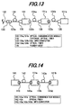
- FIG. 13 and FIG. 14 show modifications of this embodiment.
- the MPO connector 74 for the external optical fiber 76 can be attached to or detached from the front receptacle portion 75 of the optical communication module 71 .
- the modification is composed such that one end of optical fibers 134 , 134 a and 134 b is fixed to the inside of optical communication modules 131 , 131 a and 131 b . Furthermore, MPO connectors 133 a , 133 b and 133 c are attached to the other end of the optical fibers 134 , 134 a and 134 b.
- the MPO connector 133 a of the optical fiber 134 is connected to an MPO connector 133 of an external optical fiber 132 , one end of the optical fiber 134 is protected by a rubber boot 135 and fixed to the inside of the optical communication module 131 , such that it is optically connected to the front lens portion 8 .
- the optical communication modules 131 a and 131 b are arranged at appropriate intervals behind the optical communication module 131 .
- the MPO connector 133 b of the optical fiber 134 a is connected to the back side of the optical communication module 131 and one end of the optical fiber 134 a is protected by the rubber boot 135 and connected to the front side of the optical communication module 131 a .
- an MPO connector 133 c of the optical fiber 134 b is connected to the back side of the optical communication module 131 a and one end of the optical fiber 134 b is protected by the rubber boot 135 and connected to the front side of the optical communication module 131 b.
- optical communication modules 141 a and 141 b are arranged at appropriate intervals behind an optical communication module 141 .
- An MPO connector 143 of an optical fiber 142 is connected to the back side of the optical communication module 141 and an MPO connector 143 a at the other end of the optical fiber 142 is connected to the front side of the optical communication module 141 a .
- an MPO connector 143 c of an optical fiber 142 a is connected to the back side of the optical communication module 141 a and an MPO connector 143 d at the other end of the optical fiber 142 a is connected to the front side of the optical communication module 141 b.
- the plural optical communication modules may be optically connected in series using the optical fibers with the MPO connectors at both ends.
- the optical communication modules 131 and 141 can be serially connected via the optical fiber. Therefore, it is possible to freely arrange the optical communication modules on the optical communication board 81 (see FIG. 8 ).
- the MPO connector 74 for the external optical fiber 76 is attached to the top optical communication module 71 of the N optical communication modules 71 n mounted in tandem on an optical communication board 91 .
- the optical communication modules 71 in another row may be mounted on the optical communication board 91 and the external optical fiber 76 may be connected to the top of the optical communication modules 71 .
- one row of the optical communication modules 71 may be a group of optical transmitter modules and the other row may be a group of optical receiver modules.
- both rows of the optical communication modules 71 may be optical transmitter and receiver modules.
- an optical communication module 101 shown in FIG. 10 is composed of an optical package 2 , an optical filter 3 , an optical block 102 , a housing 103 , an in-housing circuit board 6 , and an electrical connector 7 .
- the housing 103 has a front receptacle portion 75 around the front lens portion 8 (see FIG. 1 ), where the front receptacle portion 75 is shaped such that it can hold the MPO connector 74 when engaged with the MPO connector 74 fitted thereinto. Furthermore, the housing 103 has a rear receptacle portion 104 around the rear lens portion 9 (see FIG. 1 ), where the rear receptacle portion 104 is shaped such that it can hold the MPO connector 74 when engaged with the MPO connector 74 fitted thereinto.
- the MPO connector 74 is also connected to the back side of the optical communication module 101 . Therefore, the optical communication module 101 operates such that light inputted from the side of the rear MPO connector 74 and light of a specific wavelength among light wavelengths emitted from the semiconductor optical device 2 in the optical communication module 101 are outputted to the side of the front MPO connector 74 .
- the optical communication modules 101 are mounted on an optical communication board 111 in an appropriate arrangement and at appropriate intervals.
- the N optical communication modules 101 are arranged in one row aligning so as to be the same front-back direction with a predetermined interval in a direction orthogonal to the front-back direction.
- the MPO connectors 74 attached to both ends of a relay optical fiber 112 are engaged with the rear receptacle portion 104 of the i-th optical communication module 101 and the front receptacle portion 75 of the i+1-th optical communication module 101 , respectively. As shown in FIG. 11 , the relay optical fiber 112 is wired being bent into an S between the two communication modules 101 .
- the rear lens portion 9 of the i-th optical communication module and the front lens portion 8 of the i+1-th optical communication module are optically connected via the relay optical fiber 112 .
- the reflection wavelength of the optical filter 3 of each optical communication module 101 is difference from each other.
- the MPO connector 74 with the external optical fiber 76 is attached to the front receptacle portion 75 of the first optical communication module 101 .
- light of different wavelengths outputted from the optical communication modules 101 is multiplexed and transmitted to the external optical fiber 76 .
- the optical communication modules 101 may be mounted on another space of the optical communication board 111 and the external optical fiber 76 may be connected to the top of the optical communication modules 101 .
Abstract
Description
- (1) According to one embodiment of the invention, an optical communication module comprises:
- (2) According to another embodiment of the invention, a method for using the optical communication module according to the embodiment (1) comprises:
Claims (15)
Applications Claiming Priority (2)
| Application Number | Priority Date | Filing Date | Title |
|---|---|---|---|
| JP2008-031598 | 2008-02-13 | ||
| JP2008031598A JP4872941B2 (en) | 2008-02-13 | 2008-02-13 | Optical communication module and method of using the same |
Publications (2)
| Publication Number | Publication Date |
|---|---|
| US20090202252A1 US20090202252A1 (en) | 2009-08-13 |
| US8401396B2 true US8401396B2 (en) | 2013-03-19 |
Family
ID=40938967
Family Applications (1)
| Application Number | Title | Priority Date | Filing Date |
|---|---|---|---|
| US12/230,950 Expired - Fee Related US8401396B2 (en) | 2008-02-13 | 2008-09-08 | Optical communication module and method for using the same |
Country Status (2)
| Country | Link |
|---|---|
| US (1) | US8401396B2 (en) |
| JP (1) | JP4872941B2 (en) |
Families Citing this family (9)
| Publication number | Priority date | Publication date | Assignee | Title |
|---|---|---|---|---|
| US9239440B2 (en) * | 2010-11-09 | 2016-01-19 | Corning Incorporated | Receptacle ferrules with monolithic lens system and fiber optic connectors using same |
| TWI530723B (en) * | 2012-03-20 | 2016-04-21 | 鴻海精密工業股份有限公司 | Optical transmission system |
| JP5958364B2 (en) * | 2013-01-28 | 2016-07-27 | 日立金属株式会社 | Optical module |
| WO2016048825A1 (en) | 2014-09-23 | 2016-03-31 | Corning Optical Communications LLC | Optical connectors and complimentary optical receptacles having magnetic attachment |
| WO2016114335A1 (en) * | 2015-01-15 | 2016-07-21 | コニカミノルタ株式会社 | Optical element and manufacturing method for optical element |
| CN107111008A (en) * | 2015-01-15 | 2017-08-29 | 柯尼卡美能达株式会社 | The manufacture method of optical element and optical element |
| KR102028193B1 (en) * | 2015-11-04 | 2019-10-04 | 한국전자통신연구원 | Single module bi-directional optical transmitting and receiving System |
| US9733438B2 (en) * | 2015-11-05 | 2017-08-15 | Sae Magnetics (H.K.) Ltd. | Optical connector for data transceiver modules and lens block for optical connectors |
| KR101825188B1 (en) * | 2016-04-19 | 2018-02-02 | 옵티시스 주식회사 | Sensor module having sensor package |
Citations (8)
| Publication number | Priority date | Publication date | Assignee | Title |
|---|---|---|---|---|
| JPH11149953A (en) | 1997-11-18 | 1999-06-02 | Mitsubishi Electric Corp | Electronic device |
| US6034821A (en) | 1997-09-05 | 2000-03-07 | Nec Research Institute, Inc. | Optomechanical components for use as optical interconnects |
| US6334716B1 (en) * | 1998-12-11 | 2002-01-01 | Fujitsu Limited | Optical transmit/receive module and method of fabricating the same |
| US20020176667A1 (en) * | 2001-05-23 | 2002-11-28 | Lutz Melchior | Module for optical signal transmission |
| US20030063844A1 (en) | 2001-09-28 | 2003-04-03 | Caracci Stephen J. | Optical signal device |
| US6722793B2 (en) * | 2000-08-03 | 2004-04-20 | Infineon Technologies Ag | Optical bidirectional transceiver module having a pin element with integrated WDM filter |
| US20040240805A1 (en) * | 2003-03-19 | 2004-12-02 | Daryoosh Vakhshoori | Assembly of optical components and method for assembling same |
| JP2005315992A (en) | 2004-04-27 | 2005-11-10 | Murata Mfg Co Ltd | Optical transceiver structure |
-
2008
- 2008-02-13 JP JP2008031598A patent/JP4872941B2/en not_active Expired - Fee Related
- 2008-09-08 US US12/230,950 patent/US8401396B2/en not_active Expired - Fee Related
Patent Citations (9)
| Publication number | Priority date | Publication date | Assignee | Title |
|---|---|---|---|---|
| US6034821A (en) | 1997-09-05 | 2000-03-07 | Nec Research Institute, Inc. | Optomechanical components for use as optical interconnects |
| JPH11149953A (en) | 1997-11-18 | 1999-06-02 | Mitsubishi Electric Corp | Electronic device |
| US6334716B1 (en) * | 1998-12-11 | 2002-01-01 | Fujitsu Limited | Optical transmit/receive module and method of fabricating the same |
| US6722793B2 (en) * | 2000-08-03 | 2004-04-20 | Infineon Technologies Ag | Optical bidirectional transceiver module having a pin element with integrated WDM filter |
| US20020176667A1 (en) * | 2001-05-23 | 2002-11-28 | Lutz Melchior | Module for optical signal transmission |
| US20030063844A1 (en) | 2001-09-28 | 2003-04-03 | Caracci Stephen J. | Optical signal device |
| WO2003029857A1 (en) | 2001-09-28 | 2003-04-10 | Corning Incorporated | Optical signal device |
| US20040240805A1 (en) * | 2003-03-19 | 2004-12-02 | Daryoosh Vakhshoori | Assembly of optical components and method for assembling same |
| JP2005315992A (en) | 2004-04-27 | 2005-11-10 | Murata Mfg Co Ltd | Optical transceiver structure |
Non-Patent Citations (1)
| Title |
|---|
| Notification of Reason(s) for Refusal dated Aug. 2, 2011, with English translation. |
Also Published As
| Publication number | Publication date |
|---|---|
| JP2009192683A (en) | 2009-08-27 |
| JP4872941B2 (en) | 2012-02-08 |
| US20090202252A1 (en) | 2009-08-13 |
Similar Documents
| Publication | Publication Date | Title |
|---|---|---|
| US8401396B2 (en) | Optical communication module and method for using the same | |
| US10215928B2 (en) | Unitary fiber optic ferrule and adapter therefor | |
| US10732353B2 (en) | Wavelength multiplexing optical module, wavelength demultiplexing optical module, and optical module | |
| JP4983703B2 (en) | Optical transmission system | |
| US10270531B2 (en) | Optical transceiver and method of manufacturing the same | |
| US20080226228A1 (en) | Optical system connection structure, optical component, and optical communication module | |
| US9588307B2 (en) | Parallel optical transceiver with top and bottom lenses | |
| EP2402804B1 (en) | Optical communication module and optical communication connector | |
| US20100008675A1 (en) | Integrated transceiver with lightpipe coupler | |
| US20080247713A1 (en) | Optical transmission module and optical patch cable | |
| US9097864B2 (en) | Fiber optic connector assemblies having a reverse optical fiber loop | |
| JP2012018363A (en) | Lens array and optical module comprising the same | |
| CN107209334B (en) | Optical receptacle and optical module | |
| CN108693607B (en) | Optical communication module and bidirectional optical communication module | |
| US20150098680A1 (en) | Optically connecting a chip package to an optical connector | |
| US9606305B1 (en) | Optical engine for data communication | |
| US8731347B2 (en) | Lens standoff and protection for optical communication systems | |
| US11415763B2 (en) | Rigid-plane optical jumper for pluggable optical transceivers | |
| US9977202B2 (en) | Optical multichannel transmission and/or reception module, in particular for high-bitrate digital optical signals | |
| WO2015153321A1 (en) | Substrate mounted optical receptacle | |
| US11409060B2 (en) | Optical module | |
| US20150381278A1 (en) | Low-profile optical transceiver system with top and bottom lenses | |
| CN112130263B (en) | High density optical transceiver assembly | |
| EP3546998A1 (en) | Optical module and manufacturing method for optical module | |
| JP2010122495A (en) | Optical communication module |
Legal Events
| Date | Code | Title | Description |
|---|---|---|---|
| AS | Assignment |
Owner name: HITACHI CABLE, LTD., JAPAN Free format text: ASSIGNMENT OF ASSIGNORS INTEREST;ASSIGNORS:SUNAGA, YOSHINORI;TAMURA, KENICHI;ISHIGAMI, YOSHIAKI;REEL/FRAME:022091/0294 Effective date: 20080925 |
|
| STCF | Information on status: patent grant |
Free format text: PATENTED CASE |
|
| FPAY | Fee payment |
Year of fee payment: 4 |
|
| AS | Assignment |
Owner name: HITACHI METALS, LTD., JAPAN Free format text: MERGER;ASSIGNOR:HITACHI CABLE, LTD.;REEL/FRAME:040424/0451 Effective date: 20130701 |
|
| FEPP | Fee payment procedure |
Free format text: MAINTENANCE FEE REMINDER MAILED (ORIGINAL EVENT CODE: REM.); ENTITY STATUS OF PATENT OWNER: LARGE ENTITY |
|
| LAPS | Lapse for failure to pay maintenance fees |
Free format text: PATENT EXPIRED FOR FAILURE TO PAY MAINTENANCE FEES (ORIGINAL EVENT CODE: EXP.); ENTITY STATUS OF PATENT OWNER: LARGE ENTITY |
|
| STCH | Information on status: patent discontinuation |
Free format text: PATENT EXPIRED DUE TO NONPAYMENT OF MAINTENANCE FEES UNDER 37 CFR 1.362 |
|
| FP | Lapsed due to failure to pay maintenance fee |
Effective date: 20210319 |