US8378486B2 - Semiconductor device and method of manufacturing semiconductor device - Google Patents
Semiconductor device and method of manufacturing semiconductor device Download PDFInfo
- Publication number
- US8378486B2 US8378486B2 US12/923,885 US92388510A US8378486B2 US 8378486 B2 US8378486 B2 US 8378486B2 US 92388510 A US92388510 A US 92388510A US 8378486 B2 US8378486 B2 US 8378486B2
- Authority
- US
- United States
- Prior art keywords
- resin layer
- conductive
- semiconductor device
- bump
- insulating resin
- Prior art date
- Legal status (The legal status is an assumption and is not a legal conclusion. Google has not performed a legal analysis and makes no representation as to the accuracy of the status listed.)
- Expired - Fee Related, expires
Links
Images


Classifications
-
- H10W72/012—
-
- H10W72/20—
-
- H10W72/90—
-
- H10W70/654—
-
- H10W72/01215—
-
- H10W72/01231—
-
- H10W72/01251—
-
- H10W72/01261—
-
- H10W72/221—
-
- H10W72/222—
-
- H10W72/223—
-
- H10W72/225—
-
- H10W72/234—
-
- H10W72/244—
-
- H10W72/245—
-
- H10W72/247—
-
- H10W72/248—
-
- H10W72/251—
-
- H10W72/253—
-
- H10W72/255—
-
- H10W72/29—
-
- H10W74/129—
Definitions
- the present invention relates to a semiconductor device having a bump in which a conductive film is formed on a bump core made of resin and a method of manufacturing the semiconductor device.
- a bump is formed in a semiconductor device in order to mount a semiconductor device on the mounting board.
- a circuit included in the semiconductor device is connected to an electrode such as the land of the mounting board through this bump.
- the core of the bump is formed of a resin, and the bump is formed by forming a conductive film on this core.
- Japanese Unexamined patent publication NO. 2007-201106 discloses a technique for dispersing conductive metal particles in a resin forming the bump core. According to this technique, it has been known that even when a crack or a fissure is generated in a conductive film, it is possible to suppress lowering of the reliability of the electrical connection between the bump and the electrode.
- the conductive metal particles are dispersed throughout the whole bump core.
- the bumps are brought into close contact with each other, the lower portions of the bump core are connected to each other.
- the conductive metal particles are dispersed throughout the whole bump core, the bumps adjacent to each other are short-circuited through the bump core.
- a semiconductor device including: a protective insulating film; an opening formed in the protective insulating film; an electrode pad located within the opening; a bump, formed over the protective insulating film, that includes a bump core and a conductive film formed over the bump core; and an interconnect that connects the conductive film of the bump and the electrode pad, wherein the bump core includes an insulating resin layer, and a conductive resin layer located over the insulating resin layer.
- a place in which a crack is generated in the conductive film forming the bump is a portion located on the upper portion of the bump core, for example, a portion located at a region of the boundary between the upper surface and the side of the bump core.
- the bump core has a configuration in which the conductive resin layer is laminated on the insulating resin layer. That is, the upper portion of the bump core is formed by the conductive resin layer. For this reason, even when a crack exists in the conductive film, electrical reliability of the bump is secured by a portion formed by the conductive resin layer in the bump core.
- the lower portions of the bump core of the adjacent bumps are formed to be connected to each other, the lower portions of the bump core are formed by the insulating resin layer, which results in suppression of electrical short-circuit of the adjacent bumps. Therefore, according to the invention, it is possible to make the bump pitch narrower without short-circuiting between the adjacent bumps, while suppressing lowering of the electrical reliability of the bump.
- a method of manufacturing a semiconductor device including forming a bump in a substrate including a protective insulating film, an opening formed in the protective insulating film, and an electrode pad exposed from the opening, the method including: forming an insulating resin layer over the protective insulating film; forming a conductive resin layer over the insulating resin layer; forming a bump core by selectively removing a laminated film of the insulating resin layer and the conductive resin layer; and forming the bump and an interconnect that connects the bump to the electrode pad by selectively forming a conductive film over the bump core, the protective insulating film, and the electrode pad.
- the semiconductor device having the bump with the bump core it is possible to make the bump pitch narrower without short-circuiting between the adjacent bumps, while suppressing lowering of the electrical reliability of the bump.
- FIGS. 1A and 1B are cross-sectional views illustrating a method of manufacturing a semiconductor device according to a first embodiment
- FIGS. 2A and 2B are cross-sectional views illustrating the method of manufacturing the semiconductor device according to the first embodiment
- FIGS. 3A and 3B are cross-sectional views illustrating the method of manufacturing the semiconductor device according to the first embodiment
- FIG. 4 is a plan view of the semiconductor device shown in FIG. 3A ;
- FIG. 5 is a cross-sectional view taken along the line B-B′ in FIG. 4 ;
- FIG. 6 is a diagram for explaining the operation and the effect of the first embodiment
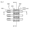
- FIG. 7 is a plan view illustrating the configuration of the semiconductor device according to a second embodiment.
- FIG. 8 is a cross-sectional view taken along the line B-B′ in FIG. 7 .
- FIG. 1A to FIG. 3B are cross-sectional views illustrating a method of manufacturing a semiconductor device according to a first embodiment.
- the method of manufacturing the semiconductor device includes a process of forming a bump in a substrate 100 having a protective insulating film 120 , an opening 122 formed in the protective insulating film 120 , and an electrode pad 130 exposed from the opening 122 .
- an insulating resin layer 212 is formed on the protective insulating film 120 .
- a conductive resin layer 214 is formed on the insulating resin layer 212 .
- a bump core 210 is formed by selectively removing the laminated film of the insulating resin layer 212 and the conductive resin layer 214 .
- a bump 200 and an interconnect 230 are formed by selectively forming a conductive film on the bump core 210 , the protective insulating film 120 , and the electrode pad 130 .
- The'interconnect 230 connects the bump 200 to the electrode pad 130 .
- elements such as a transistor, are formed on the substrate 100 , and a multilayered interconnect layer 110 is further formed on the substrate 100 .
- the electrode pad 130 is formed in an interconnect layer located at the uppermost layer of the multilayered interconnect layer 110 .
- the protective insulating film 120 is formed on the multilayered interconnect layer 110 .
- the opening 122 is formed by selectively removing the protective insulating film 120 .
- the opening 122 is located on the electrode pad 130 , and exposes the electrode pad 130 from the protective insulating film 120 .
- the insulating resin layer 212 is formed on the protective insulating film 120 and the electrode pad 130 .
- the insulating resin layer 212 is formed of, for example, a thermosetting resin such as a phenol resin, an epoxy resin, a polyimide resin, an amino resin, an unsaturated polyester resin, a silicon resin, or an allyl resin, or a photo-curable resin such as a silicone-based resin or an imide-based resin.
- the conductive resin layer 214 has a configuration in which conductive powder, for example, particles are mixed in an insulating base material.
- the base material of the conductive resin layer 214 is, for example, a thermosetting resin such as a phenol resin, an epoxy resin, a polyimide resin, an amino resin, an unsaturated polyester resin, a silicon resin, or an allyl resin, or a photo-curable resin such a silicone-based resin or an imide-based resin. It is preferable that the base material of the conductive resin layer 214 is the same resin as the resin forming the insulating resin layer 212 .
- the insulating resin layer 212 and the conductive resin layer 214 are exposed and developed. Thereby, the insulating resin layer 212 and the conductive resin layer 214 are selectively removed, and remain on the protective insulating film 120 in an island shape.
- the conductive resin layer 214 has a configuration in which conductive powder, for example, metallic powder are mixed in a photosensitive resin. As shown in FIG. 2A , in the state after selective removal thereof, the area of the conductive resin layer 214 , when seen in a plan view, is made smaller than that of the insulating resin layer 212 . In order to obtain such a configuration, there is a method of, for example', adjusting the type and quantity of a photosensitizing agent, a solvent, and an additive agent of the resin of each layer.
- the area of the conductive resin layer 214 is made smaller than that of the insulating resin layer 212 , it is possible to improve coatability of the conductive film with respect to the bump core 210 at the time of forming a conductive film 220 described later.
- the area of the conductive resin layer 214 may be the same as the area of the insulating resin layer 212 .
- the insulating resin layer 212 and the conductive resin layer 214 are cured.
- This process is a process of heat-treating the insulating resin layer 212 and the conductive resin layer 214 when the insulating resin layer 212 and the conductive resin layer 214 are thermosetting resins, and a process of irradiating the insulating resin layer 212 and the conductive resin layer 214 with light when the insulating resin layer 212 and the conductive resin layer 214 are photo-curable resins.
- the bump core 210 is formed on the protective insulating film 120 .
- the bump core 210 is formed by the insulating resin layer 212 and the conductive resin layer 214 .
- a conductive film for example, an Au film is formed on the bump core 210 , the protective insulating film 120 , and the electrode pad 130 by, for example, a sputtering method.
- a resist pattern (not shown) is formed on the conductive film, and the conductive film is etched using this resist pattern as a mask. Thereby, the conductive film is selectively removed, and the conductive film 220 for forming the bump 200 , and the interconnect 230 are formed.
- the bump 200 has a configuration in which the conductive film 220 is formed on the bump core 210 .
- the interconnect 230 is stretched from the conductive film 220 of the bump 200 onto the protective insulating film 120 , and connects the conductive film 220 of the bump 200 to the electrode pad 130 . After that, the resist pattern is removed.
- the semiconductor device thus formed includes the protective insulating film 120 , the opening 122 formed in the protective insulating film 120 , the electrode pad 130 located within the opening 122 , the bump 200 formed on the protective insulating film 120 , and the interconnect 230 .
- the bump 200 includes the bump core 210 and the conductive film 220 .
- the bump core 210 includes the insulating resin layer 212 , and the conductive resin layer 214 located on the insulating resin layer 212 .
- the conductive film 220 is formed on at least the upper surface of the bump core 210 .
- the interconnect 230 connects the conductive film 220 of the bump 200 and the electrode pad 130 .
- the thickness of the conductive resin layer 214 is equal to or greater than the thickness of the conductive film 220 . In addition, it is preferable that the thickness of the conductive resin layer 214 is equal to or less than 90% of the height h 1 (see FIG. 5 ) of the bump core 210 . These reasons will be described.
- the thickness of the conductive resin layer 214 is at least the thickness of the conductive film 220 in the vicinity of the vertex portion of the bump 200 .
- the thickness of the conductive resin layer 214 is equal to or less than 90% of the height h 1 of the bump core 210 . Meanwhile, there may be a case where it is necessary to make the thickness of the conductive resin layer 214 smaller, for example, to set the thickness thereof to be equal to or less than 50% of the height h 1 of the bump core 210 , due to the swelling characteristics of the resin or the mounting pressure.
- chip on glass (COG) mounting or chip on film (COF) mounting of the semiconductor device in a mounting board 300 is performed.
- the semiconductor device is a liquid crystal driver
- the mounting board 300 is a glass substrate.
- the bump 200 of the semiconductor device is connected to an electrode 310 of the mounting board 300 .
- the electrode 310 is, for example a land, but is not limited to the land.
- FIG. 4 is a plan view of the semiconductor device shown in FIG. 3A
- FIG. 5 is a cross-sectional view taken along the line B-B′ in FIG. 4
- FIG. 3A is a cross-sectional view taken along the line A-A′ in FIG. 4
- a plurality of bumps 200 is disposed along a first direction (vertical direction in the drawings).
- the interconnect 230 is stretched in a second direction different from the first direction, for example, a direction (horizontal direction in the drawings) perpendicular to the first direction.
- a plurality of bumps 200 is separated from each other, but is disposed close to each other.
- the conductive film 220 of the bump 200 is not formed in a portion directed in the above-mentioned first direction among the sides of the bump core 210 .
- the conductive film 220 may be formed in a region which is formed by the conductive resin layer 214 among these sides.
- a crack 232 is easily generated at a portion located on the upper portion of the bump core 210 , for example, a portion located in a region of a boundary between the upper surface and the side of the bump core 210 , in the conductive film 220 forming the bump 200 .
- the upper portion of the bump core 210 is formed by the conductive resin layer 214 .
- the lower portion of the bump core 210 is formed by the insulating resin layer 212 . For this reason, even when a plurality of bumps 200 is disposed close to each other, and the adjacent bump cores 210 are connected to each other at the lower portion at the time of forming the bump core 210 , electrical conduction between the bumps 200 adjacent to each other through the bump cores 210 is suppressed.
- FIG. 7 is a plan view illustrating the configuration of the semiconductor device according to a second embodiment
- FIG. 8 is a cross-sectional view taken along the B-B′ in FIG. 7 .
- the cross section of the line A-A′ in FIG. 7 is the same as that shown in FIGS. 3A and 3B in the first embodiment.
- the semiconductor device according to the embodiment is the same as the semiconductor device according to the first embodiment, with the exception that a plurality of bumps 200 is close to each other, and at least the lower portions of the insulating resin layer 212 of the bump core 210 are connected to each other.
- a method of manufacturing this semiconductor device is the same as that of the first embodiment.
- the thickness of the conductive resin layer 214 is equal to or greater than the thickness of the conductive film 220 . In addition, it is preferable that the thickness of the conductive resin layer 214 is equal to or less than 90% of the height h 2 of the vertex portion of the bump core 210 based on the segregation point of the adjacent bump cores 210 .
- the semiconductor device can be made smaller.
Landscapes
- Internal Circuitry In Semiconductor Integrated Circuit Devices (AREA)
Abstract
Description
Claims (20)
Applications Claiming Priority (2)
| Application Number | Priority Date | Filing Date | Title |
|---|---|---|---|
| JP2009246813A JP5386302B2 (en) | 2009-10-27 | 2009-10-27 | Semiconductor device and manufacturing method of semiconductor device |
| JP2009-246813 | 2009-10-27 |
Publications (2)
| Publication Number | Publication Date |
|---|---|
| US20110095420A1 US20110095420A1 (en) | 2011-04-28 |
| US8378486B2 true US8378486B2 (en) | 2013-02-19 |
Family
ID=43897690
Family Applications (1)
| Application Number | Title | Priority Date | Filing Date |
|---|---|---|---|
| US12/923,885 Expired - Fee Related US8378486B2 (en) | 2009-10-27 | 2010-10-13 | Semiconductor device and method of manufacturing semiconductor device |
Country Status (3)
| Country | Link |
|---|---|
| US (1) | US8378486B2 (en) |
| JP (1) | JP5386302B2 (en) |
| CN (1) | CN102054789B (en) |
Families Citing this family (1)
| Publication number | Priority date | Publication date | Assignee | Title |
|---|---|---|---|---|
| US9728517B2 (en) * | 2013-12-17 | 2017-08-08 | Taiwan Semiconductor Manufacturing Company Ltd. | Semiconductor device and manufacturing method thereof |
Citations (4)
| Publication number | Priority date | Publication date | Assignee | Title |
|---|---|---|---|---|
| US4813129A (en) * | 1987-06-19 | 1989-03-21 | Hewlett-Packard Company | Interconnect structure for PC boards and integrated circuits |
| US20060237842A1 (en) * | 2003-10-09 | 2006-10-26 | Seiko Epson Corporation | Semiconductor device including an under electrode and a bump electrode |
| US20060288572A1 (en) * | 2005-06-28 | 2006-12-28 | Seiko Epson Corporation | Method of manufacturing semiconductor device |
| JP2007201106A (en) | 2006-01-25 | 2007-08-09 | Fujitsu Ltd | Semiconductor element connection bump and semiconductor device |
Family Cites Families (5)
| Publication number | Priority date | Publication date | Assignee | Title |
|---|---|---|---|---|
| JP2833996B2 (en) * | 1994-05-25 | 1998-12-09 | 日本電気株式会社 | Flexible film and semiconductor device having the same |
| US6284563B1 (en) * | 1995-10-31 | 2001-09-04 | Tessera, Inc. | Method of making compliant microelectronic assemblies |
| JP3450238B2 (en) * | 1999-11-04 | 2003-09-22 | Necエレクトロニクス株式会社 | Semiconductor device and manufacturing method thereof |
| JP3938128B2 (en) * | 2003-09-30 | 2007-06-27 | セイコーエプソン株式会社 | SEMICONDUCTOR DEVICE AND ITS MANUFACTURING METHOD, CIRCUIT BOARD, ELECTRO-OPTICAL DEVICE, AND ELECTRONIC DEVICE |
| JP4151634B2 (en) * | 2004-09-24 | 2008-09-17 | セイコーエプソン株式会社 | SEMICONDUCTOR DEVICE AND ITS MANUFACTURING METHOD, CIRCUIT BOARD, ELECTRO-OPTICAL DEVICE, AND ELECTRONIC DEVICE |
-
2009
- 2009-10-27 JP JP2009246813A patent/JP5386302B2/en not_active Expired - Fee Related
-
2010
- 2010-10-13 US US12/923,885 patent/US8378486B2/en not_active Expired - Fee Related
- 2010-10-20 CN CN201010516547.9A patent/CN102054789B/en not_active Expired - Fee Related
Patent Citations (4)
| Publication number | Priority date | Publication date | Assignee | Title |
|---|---|---|---|---|
| US4813129A (en) * | 1987-06-19 | 1989-03-21 | Hewlett-Packard Company | Interconnect structure for PC boards and integrated circuits |
| US20060237842A1 (en) * | 2003-10-09 | 2006-10-26 | Seiko Epson Corporation | Semiconductor device including an under electrode and a bump electrode |
| US20060288572A1 (en) * | 2005-06-28 | 2006-12-28 | Seiko Epson Corporation | Method of manufacturing semiconductor device |
| JP2007201106A (en) | 2006-01-25 | 2007-08-09 | Fujitsu Ltd | Semiconductor element connection bump and semiconductor device |
Also Published As
| Publication number | Publication date |
|---|---|
| CN102054789A (en) | 2011-05-11 |
| JP2011096729A (en) | 2011-05-12 |
| CN102054789B (en) | 2014-12-24 |
| US20110095420A1 (en) | 2011-04-28 |
| JP5386302B2 (en) | 2014-01-15 |
Similar Documents
| Publication | Publication Date | Title |
|---|---|---|
| CN1118088C (en) | Semiconductor apparatus and method for fabricating the same | |
| TWI609467B (en) | Package structure and method of forming package structure | |
| CN2585416Y (en) | Semiconductor chip and wiring substrate, semiconductor wafer, semiconductor device, wire substrate and electronic machine | |
| US8304905B2 (en) | Semiconductor device | |
| CN107993987B (en) | Package-to-board interconnect structure with built-in reference plane structure | |
| US20130127048A1 (en) | Device | |
| KR20020052223A (en) | Semiconductor module | |
| US20080169555A1 (en) | Anchor structure for an integrated circuit | |
| EP2229694A2 (en) | Under bump routing layer method and apparatus | |
| CN1211835C (en) | Method for forming buffer pad, semiconductor device and making method, circuit substrate and electronic equipment | |
| JP5243735B2 (en) | Circuit board and semiconductor device | |
| JP5272729B2 (en) | Semiconductor package and semiconductor package manufacturing method | |
| US20060115927A1 (en) | Attachment of flip chips to substrates | |
| US7382057B2 (en) | Surface structure of flip chip substrate | |
| US20110133338A1 (en) | Conductor bump method and apparatus | |
| CN1193417C (en) | Method for manufacturing a circuit device | |
| US20050148165A1 (en) | Conductive pattern producing method and its applications | |
| US8378486B2 (en) | Semiconductor device and method of manufacturing semiconductor device | |
| US9408313B2 (en) | Packaging substrate and method of fabricating the same | |
| JP2020077696A (en) | Wiring board and semiconductor device using the same | |
| US20110059606A1 (en) | Method of manufacturing semiconductor device and mask | |
| US20240170432A1 (en) | Semiconductor device | |
| US11917756B2 (en) | Printed wiring board and method for manufacturing printed wiring board | |
| KR20080043068A (en) | Semiconductor device having chip on film structure and manufacturing method | |
| US20250168984A1 (en) | Printed circuit board and semiconductor package including the same |
Legal Events
| Date | Code | Title | Description |
|---|---|---|---|
| AS | Assignment |
Owner name: RENESAS ELECTRONICS CORPORATION, JAPAN Free format text: ASSIGNMENT OF ASSIGNORS INTEREST;ASSIGNOR:BEKKU, FUMIHIRO;REEL/FRAME:025194/0700 Effective date: 20100916 |
|
| STCF | Information on status: patent grant |
Free format text: PATENTED CASE |
|
| FPAY | Fee payment |
Year of fee payment: 4 |
|
| AS | Assignment |
Owner name: RENESAS ELECTRONICS CORPORATION, JAPAN Free format text: CHANGE OF ADDRESS;ASSIGNOR:RENESAS ELECTRONICS CORPORATION;REEL/FRAME:044928/0001 Effective date: 20150806 |
|
| FEPP | Fee payment procedure |
Free format text: MAINTENANCE FEE REMINDER MAILED (ORIGINAL EVENT CODE: REM.); ENTITY STATUS OF PATENT OWNER: LARGE ENTITY |
|
| LAPS | Lapse for failure to pay maintenance fees |
Free format text: PATENT EXPIRED FOR FAILURE TO PAY MAINTENANCE FEES (ORIGINAL EVENT CODE: EXP.); ENTITY STATUS OF PATENT OWNER: LARGE ENTITY |
|
| STCH | Information on status: patent discontinuation |
Free format text: PATENT EXPIRED DUE TO NONPAYMENT OF MAINTENANCE FEES UNDER 37 CFR 1.362 |
|
| FP | Lapsed due to failure to pay maintenance fee |
Effective date: 20210219 |