US8344366B2 - Organic thin film transistor and method of forming the same - Google Patents
Organic thin film transistor and method of forming the same Download PDFInfo
- Publication number
- US8344366B2 US8344366B2 US12/858,868 US85886810A US8344366B2 US 8344366 B2 US8344366 B2 US 8344366B2 US 85886810 A US85886810 A US 85886810A US 8344366 B2 US8344366 B2 US 8344366B2
- Authority
- US
- United States
- Prior art keywords
- forming
- gate dielectric
- electrode
- recess region
- gate
- Prior art date
- Legal status (The legal status is an assumption and is not a legal conclusion. Google has not performed a legal analysis and makes no representation as to the accuracy of the status listed.)
- Expired - Fee Related, expires
Links
Images


Classifications
-
- H—ELECTRICITY
- H10—SEMICONDUCTOR DEVICES; ELECTRIC SOLID-STATE DEVICES NOT OTHERWISE PROVIDED FOR
- H10K—ORGANIC ELECTRIC SOLID-STATE DEVICES
- H10K10/00—Organic devices specially adapted for rectifying, amplifying, oscillating or switching; Organic capacitors or resistors having potential barriers
- H10K10/80—Constructional details
- H10K10/82—Electrodes
- H10K10/84—Ohmic electrodes, e.g. source or drain electrodes
-
- H—ELECTRICITY
- H10—SEMICONDUCTOR DEVICES; ELECTRIC SOLID-STATE DEVICES NOT OTHERWISE PROVIDED FOR
- H10K—ORGANIC ELECTRIC SOLID-STATE DEVICES
- H10K10/00—Organic devices specially adapted for rectifying, amplifying, oscillating or switching; Organic capacitors or resistors having potential barriers
- H10K10/40—Organic transistors
- H10K10/46—Field-effect transistors, e.g. organic thin-film transistors [OTFT]
- H10K10/462—Insulated gate field-effect transistors [IGFETs]
- H10K10/466—Lateral bottom-gate IGFETs comprising only a single gate
-
- H—ELECTRICITY
- H10—SEMICONDUCTOR DEVICES; ELECTRIC SOLID-STATE DEVICES NOT OTHERWISE PROVIDED FOR
- H10K—ORGANIC ELECTRIC SOLID-STATE DEVICES
- H10K10/00—Organic devices specially adapted for rectifying, amplifying, oscillating or switching; Organic capacitors or resistors having potential barriers
- H10K10/40—Organic transistors
- H10K10/46—Field-effect transistors, e.g. organic thin-film transistors [OTFT]
- H10K10/462—Insulated gate field-effect transistors [IGFETs]
- H10K10/468—Insulated gate field-effect transistors [IGFETs] characterised by the gate dielectrics
-
- H—ELECTRICITY
- H10—SEMICONDUCTOR DEVICES; ELECTRIC SOLID-STATE DEVICES NOT OTHERWISE PROVIDED FOR
- H10K—ORGANIC ELECTRIC SOLID-STATE DEVICES
- H10K71/00—Manufacture or treatment specially adapted for the organic devices covered by this subclass
- H10K71/10—Deposition of organic active material
- H10K71/12—Deposition of organic active material using liquid deposition, e.g. spin coating
- H10K71/13—Deposition of organic active material using liquid deposition, e.g. spin coating using printing techniques, e.g. ink-jet printing or screen printing
- H10K71/135—Deposition of organic active material using liquid deposition, e.g. spin coating using printing techniques, e.g. ink-jet printing or screen printing using ink-jet printing
-
- H—ELECTRICITY
- H10—SEMICONDUCTOR DEVICES; ELECTRIC SOLID-STATE DEVICES NOT OTHERWISE PROVIDED FOR
- H10K—ORGANIC ELECTRIC SOLID-STATE DEVICES
- H10K71/00—Manufacture or treatment specially adapted for the organic devices covered by this subclass
- H10K71/60—Forming conductive regions or layers, e.g. electrodes
- H10K71/611—Forming conductive regions or layers, e.g. electrodes using printing deposition, e.g. ink jet printing
Definitions
- the present invention disclosed herein relates to a transistor and a method of forming the same, and more particularly, to an organic thin film transistor and a method of forming the same.
- the organic semiconductor layer is formed in various and flexible synthesis methods and it is formed at relatively low cost. Moreover, since the organic semiconductor layer may be easily formed in a printing process, it may be applied to large-area devices. Because of these features, attempts are being continuously made for applying the organic semiconductor layer to electronic products such as flexible displays and Radio Frequency Identification (RFID) tags.
- RFID Radio Frequency Identification
- Typical organic thin film transistors may operate at a high operating voltage, for example, 20 V or higher. This is caused by the thickness of a gate dielectric, which may commonly have a large thickness of 100 nm or more.
- Embodiments of the present invention provide a method of forming organic thin film transistor including: forming a gate electrode on a substrate; forming a gate dielectric, which covers the gate electrode and includes a recess region at an upper portion, on the substrate; forming a source electrode and a drain electrode in the recess region; and forming an organic semiconductor layer between the source electrode and the drain electrode in the recess region.
- the forming of a gate dielectric may include: forming an auxiliary gate dielectric on the substrate; and performing an imprinting process with a mold having a convex portion to form the recess region at an upper portion of the auxiliary gate dielectric.
- the forming of a gate dielectric may further include curing the auxiliary gate dielectric after forming the recess region.
- the forming of a gate dielectric may include: forming a first gate dielectric between the gate electrode and the recess region; and forming a second gate dielectric between the substrate and the recess region, wherein a thickness of the first gate dielectric may be thinner than a thickness of the second gate dielectric, and a thickness of the auxiliary gate dielectric is thicker than a thickness of the second gate dielectric.
- the auxiliary gate dielectric may be formed of an organic insulator.
- the forming of a source electrode and a drain electrode may include: forming a conductive layer in the recess region; and curing a conductive layer which is formed at both sides of the gate electrode.
- the curing of a conductive layer may include performing an exposure process on the conductive layer by using the gate electrode as a mask.
- the gate dielectric may be formed of an ultraviolet-transmissive insulating material.
- the source electrode and the drain electrode may be formed so as to be self-aligned with the gate electrode.
- the conductive layer may be formed of an ink of conductivity.
- the conductive layer may be formed in an inkjet printing process.
- the forming of the source electrode and the drain electrode may further include removing the conductive layer between the source electrode and the drain electrode after curing the conductive layer.
- the organic semiconductor layer may be formed so as to be self-aligned with the source electrode and the drain electrode.
- the organic semiconductor layer may be formed in an inkjet printing process.
- an organic thin film transistor includes: a gate electrode on a substrate; a gate dielectric covering the gate electrode and including a recess region at an upper portion, on the substrate; a source electrode and a drain electrode disposed in the recess region; and an organic semiconductor layer disposed between the source electrode and the drain electrode in the recess region.
- lower surfaces of the source electrode, the drain electrode and the organic semiconductor layer may be parallel to an upper surface of the substrate.
- the gate dielectric may include: a first gate dielectric disposed between the gate electrode and the organic semiconductor layer; a second gate dielectric disposed between the source electrode and the substrate and between the drain electrode and the substrate; and a third gate dielectric on the substrate, and including an upper surface having the same height as height of upper surfaces of the source electrode and drain electrode.
- a thickness of the third gate dielectric may be the same as a sum of a thickness of the source electrode or drain electrode, a thickness of the first gate dielectric and a thickness of the gate electrode.
- the source electrode and the drain electrode may be self-aligned with the gate electrode and disposed.
- the organic semiconductor layer may be disposed so as to be self-aligned with the source electrode and the drain electrode.
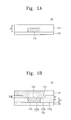
- FIGS. 1A to 1E are views for describing a method of forming organic thin film transistor according to an embodiment of the present invention
- FIG. 2 is a diagram for describing a method of forming organic thin film transistor in a roll-to-roll process according to another embodiment of the present invention.
- FIG. 3 is a diagram for describing an organic thin film transistor according to an embodiment of the present invention.
- a gate electrode 110 is formed on the substrate 100 .
- the substrate 100 may be formed as a glass substrate or a plastic substrate.
- the plastic substrate may be formed of a polymer compound such as polyimide, polyethylenenaphthalate (PEN) or polyethylene terephthalate (PET).
- the gate electrode 110 is formed by forming and patterning a conductive layer (not shown) on the substrate 100 , or it is formed in a process that covers the substrate 100 with a patterned mask and forms the conductive layer.
- the gate electrode 110 may be formed in any one of a thermal evaporation process, an E-beam evaporation process, a sputtering process, a micro contact printing process or a nano imprinting process.
- the gate electrode 110 may be formed of metal material such as aluminum (Al), chrome (Cr), molybdenum (Mo), copper (Cu), titanium (Ti) or tantalum (Ta), or it may be formed of non-metal material having conductivity.
- auxiliary gate dielectric 112 covering the gate electrode 110 is formed on the substrate 100 .
- the auxiliary gate dielectric 112 may be formed with a dispenser in a dispensing process. The dispensing process may be useful when the organic thin film transistor is formed in a roll-to-roll process. Alternatively, the auxiliary gate dielectric 112 may be formed in a spin coating process.
- the auxiliary gate dielectric 112 may substantially include a planar upper surface.
- the auxiliary gate dielectric 112 may be formed of an insulating material capable of transmitting ultraviolet.
- the auxiliary gate dielectric 112 may be formed of a material such as poly-4-vinylphenol (PVP), polyimide, polyvinylalcohol (PVA) or polystyrene (PS).
- the auxiliary gate dielectric 112 may be formed of an inorganic/organic hybrid insulating material such as Al 2 O 3 /PS.
- a recess region 105 may be formed at the upper portion of the auxiliary gate dielectric 112 by using a mold 125 including a convex portion 122 .
- a process of forming the recess region 105 may be called an imprinting process.
- the auxiliary gate dielectric 112 may have liquidity so that the recess region 105 may be formed. That is, in a state where the auxiliary gate dielectric 112 has liquidity so that a shape may be changed by the mold 125 , the shape of the convex portion 122 of the mold 125 may be carved in the auxiliary gate dielectric 112 .
- a gate dielectric 120 is formed by curing the auxiliary gate dielectric 112 .
- the gate dielectric 120 may be formed in a thermal curing process.
- the thermal curing process may be performed at a temperature lower than 200° C. Since the thermal curing process is performed at a relatively low temperature, the damage of the substrate 100 can be minimized Alternatively, the gate dielectric 120 may be cured using ultraviolet.
- the first gate dielectric 120 a is an element that determines the operating voltage of the organic thin film transistor. Since the first gate dielectric 120 a is formed to have a relatively thin thickness, the operating voltage of the organic thin film transistor can be reduced. That is, the auxiliary gate dielectric 112 is recessed, and thus the first gate dielectric 120 a having a thin thickness may be formed.
- a conductive layer 132 may be formed in the recess region 105 .
- the conductive layer 132 may be formed of an ultraviolet (UV)-curable conductive material.
- the conductive layer 132 may be formed of a paste or an ink where conductive powders such as argentums (Ag), aurum (Au), zinc (Zn), Cu, carbon nano tube and polymer are dispersed in a UV-curing resin.
- the UV-curing resin may contain a photoinitiator that reacts on UV energy.
- the conductive layer 132 is formed of a conductive ink, it may be formed in an inkjet printing process.
- the uncured conductive layer 132 is removed.
- the conductive layer 132 may be removed by a developer in a development process.
- An organic semiconductor layer 140 is formed between the source electrode 130 S and the drain electrode 130 D in the recess region 105 .
- the organic semiconductor layer 140 may be formed of any one of Tips-Pentacene[6,13-bis(triisopropylsilylethynyl)pentacene], P3HT [poly(3-hexylthiophene)], F8T2[poly (9,9-dioctylfluoreneco-bithiophene)], PQT-12[poly(3,3-didodecylquarter-thiophene) or PBTTT[poly(2,5-bis(3-tetradecylthiophen-2yl)thieno[3,2-b]thiophene).
- the organic semiconductor layer 140 may be formed in an inkjet printing process.
- the organic semiconductor layer 140 may be formed so as to be self-aligned with the source electrode 130 S and the drain electrode 130 D that have been formed in advance.
- the gate dielectric 120 (particularly, the first gate dielectric 120 a ) of the organic thin film transistor is thinly formed, thereby decreasing the operating voltage. Moreover, since the source electrode 130 S, the drain electrode 130 D and the organic semiconductor layer 140 are formed to be self-aligned, a forming process can be simplified and electrical characteristics can be improved. Since the source electrode 130 S, the drain electrode 130 D and the organic semiconductor layer 140 are formed in the recess region 105 , the entire thickness of the organic thin film transistor can be reduced and the scaling down of the device is enabled. Furthermore, the gate dielectric 120 can be thinly formed in a simple imprinting process.
- FIG. 2 is a diagram for describing a method of forming organic thin film transistor in a roll-to-roll process according to another embodiment of the present invention. Except for a difference in that an organic thin film transistor is formed in a roll-to-roll process, this embodiment is similar to the preceding embodiment. For conciseness, accordingly, a repetitive description on the same technical features will be omitted.
- S 1 , S 2 , S 3 , S 4 and S 5 indicate the processes that have been described above with reference to FIGS. 1A to 1E , respectively.
- reference numeral is omitted, and a description will be made below by referencing the reference numerals of FIGS. 1A to 1E .
- an organic thin film transistor is formed in a roll-to-roll process.
- all processes may be performed in a state where the substrate 100 is continuously conveyed.
- the substrate 100 is prepared on a roller device 50 that includes a feed roller 52 and a feed plate 54 .
- the gate electrode 110 is formed on the substrate 100 .
- the substrate 100 is conveyed by the roller device 50 , and thereby the gate dielectric 120 is formed.
- the gate dielectric 120 may be formed in a dispensing process.
- the gate dielectric 120 may be formed by forming the recess region 105 with the mold 125 (see FIG. 1B ) and being cured.
- the substrate 100 is conveyed by the roller device 50 , and the conductive layer 132 is formed in the recess region 105 of the gate dielectric 120 .
- the conductive layer 132 may be formed in an inkjet printing process.
- the conductive layer 132 is continuously exposed to UV and cured, and thereby the source electrode 130 S and the drain electrode 130 D may be self-aligned with the gate electrode 110 .
- the organic semiconductor layer 140 may be formed 105 between the source electrode 130 S and the drain electrode 130 D in the recess region.
- the organic thin film transistor can be easily formed in the roll-to-roll process, thereby saving the cost.
- FIG. 3 is a diagram for describing an organic thin film transistor according to an embodiment of the present invention.
- the gate electrode 110 is disposed on the substrate 100 .
- the substrate 100 may be a glass substrate or a plastic substrate.
- the plastic substrate may be formed of a polymer compound such as polyimide, polyethylenenaphthalate (PEN) or polyethylene terephthalate (PET).
- the gate electrode 110 may be formed of metal material such as aluminum (Al), chrome (Cr), molybdenum (Mo), copper (Cu), titanium (Ti) or tantalum (Ta), or it may be formed of non-metal material having conductivity.
- the source electrode 130 S and the drain electrode 130 D are disposed in the recess region 105 of the gate dielectric 120 .
- the source electrode 130 S and the drain electrode 130 D may include a paste, an ink or conductive materials such as argentums (Ag), aurum (Au), zinc (Zn), Cu, carbon nano tube and polymer.
- the organic semiconductor layer 140 is formed in the recess region 105 between the source electrode 130 S and the drain electrode 130 D.
- the organic semiconductor layer 140 may be formed of any one of Tips-Pentacene[6,13-bis(triisopropylsilylethynyl)pentacene], P3HT[poly(3-hexylthiophene)], F8T2[poly (9,9-dioctylfluoreneco-bithiophene)], PQT-12[poly(3,3-didodecylquarter-thiophene) or PBTTT[poly(2,5-bis(3-tetradecylthiophen-2yl)thieno[3,2-b]thiophene).
- the gate dielectric 120 may include the first gate dielectric 120 a between the gate electrode 110 and the organic semiconductor layer 140 , the second gate dielectric 120 b between the substrate 100 and the source electrode 130 S and between the substrate 100 and the drain electrode 130 D, and the third gate dielectric 120 c that is disposed on the substrate 100 and includes an upper surface having the same height as that of upper surfaces of the source electrode 130 S and drain electrode 130 D.
- a thickness t 1 of the first gate dielectric 120 a may be thinner than a thickness t 2 of the second gate dielectric 120 b.
- the first gate dielectric 120 a is an element that determines the operating voltage of the organic thin film transistor. Since the first gate dielectric 120 a is formed to have a relatively thin thickness, the operating voltage of the organic thin film transistor can be reduced. That is, the auxiliary gate dielectric 112 is recessed, and thus the first gate dielectric 120 a having a thin thickness may be disposed.
Landscapes
- Engineering & Computer Science (AREA)
- Manufacturing & Machinery (AREA)
- Thin Film Transistor (AREA)
Abstract
Description
Claims (14)
Applications Claiming Priority (2)
| Application Number | Priority Date | Filing Date | Title |
|---|---|---|---|
| KR10-2010-0015052 | 2010-02-19 | ||
| KR1020100015052A KR101309263B1 (en) | 2010-02-19 | 2010-02-19 | Organic thin film transistor and method of forming the same |
Publications (2)
| Publication Number | Publication Date |
|---|---|
| US20110204334A1 US20110204334A1 (en) | 2011-08-25 |
| US8344366B2 true US8344366B2 (en) | 2013-01-01 |
Family
ID=44464786
Family Applications (1)
| Application Number | Title | Priority Date | Filing Date |
|---|---|---|---|
| US12/858,868 Expired - Fee Related US8344366B2 (en) | 2010-02-19 | 2010-08-18 | Organic thin film transistor and method of forming the same |
Country Status (3)
| Country | Link |
|---|---|
| US (1) | US8344366B2 (en) |
| KR (1) | KR101309263B1 (en) |
| CN (1) | CN102163693A (en) |
Families Citing this family (5)
| Publication number | Priority date | Publication date | Assignee | Title |
|---|---|---|---|---|
| US9282647B2 (en) * | 2012-02-28 | 2016-03-08 | Eastman Kodak Company | Method of making micro-channel structure for micro-wires |
| CN103165471A (en) * | 2013-02-19 | 2013-06-19 | 京东方科技集团股份有限公司 | Thin film transistor and manufacture method and display device thereof |
| CN104183648B (en) * | 2014-07-25 | 2017-06-27 | 京东方科技集团股份有限公司 | A kind of thin film transistor (TFT) and preparation method thereof, array base palte and display device |
| CN105355664A (en) * | 2015-12-17 | 2016-02-24 | 深圳市华星光电技术有限公司 | Oxide thin-film transistor and manufacturing method thereof |
| EP3514822B1 (en) * | 2016-09-16 | 2023-04-26 | Toray Industries, Inc. | Method for manufacturing field effect transistor and method for manufacturing wireless communication device |
Citations (6)
| Publication number | Priority date | Publication date | Assignee | Title |
|---|---|---|---|---|
| US6207472B1 (en) | 1999-03-09 | 2001-03-27 | International Business Machines Corporation | Low temperature thin film transistor fabrication |
| KR20060078007A (en) | 2004-12-30 | 2006-07-05 | 엘지.필립스 엘시디 주식회사 | Manufacturing method of organic thin film transistor element |
| US20060284181A1 (en) * | 2005-06-21 | 2006-12-21 | Lg.Philips Lcd Co., Ltd. | Fabricating method for thin film transistor substrate and thin film transistor substrate using the same |
| KR100678771B1 (en) | 2003-09-30 | 2007-02-02 | 학교법인연세대학교 | Organic thin film transistor and its manufacturing method |
| US20080135836A1 (en) | 2004-11-09 | 2008-06-12 | Koninklijke Philips Electronics, N.V. | Self-Aligned Process To Manufacture Organic Transistors |
| KR20090045884A (en) | 2008-07-23 | 2009-05-08 | 한국기계연구원 | Self-aligned organic thin film transistor and its manufacturing method |
Family Cites Families (1)
| Publication number | Priority date | Publication date | Assignee | Title |
|---|---|---|---|---|
| KR100832873B1 (en) * | 2007-07-02 | 2008-06-02 | 한국기계연구원 | Self-aligned organic thin film transistor and its manufacturing method |
-
2010
- 2010-02-19 KR KR1020100015052A patent/KR101309263B1/en not_active Expired - Fee Related
- 2010-08-18 US US12/858,868 patent/US8344366B2/en not_active Expired - Fee Related
- 2010-08-24 CN CN2010102672255A patent/CN102163693A/en active Pending
Patent Citations (6)
| Publication number | Priority date | Publication date | Assignee | Title |
|---|---|---|---|---|
| US6207472B1 (en) | 1999-03-09 | 2001-03-27 | International Business Machines Corporation | Low temperature thin film transistor fabrication |
| KR100678771B1 (en) | 2003-09-30 | 2007-02-02 | 학교법인연세대학교 | Organic thin film transistor and its manufacturing method |
| US20080135836A1 (en) | 2004-11-09 | 2008-06-12 | Koninklijke Philips Electronics, N.V. | Self-Aligned Process To Manufacture Organic Transistors |
| KR20060078007A (en) | 2004-12-30 | 2006-07-05 | 엘지.필립스 엘시디 주식회사 | Manufacturing method of organic thin film transistor element |
| US20060284181A1 (en) * | 2005-06-21 | 2006-12-21 | Lg.Philips Lcd Co., Ltd. | Fabricating method for thin film transistor substrate and thin film transistor substrate using the same |
| KR20090045884A (en) | 2008-07-23 | 2009-05-08 | 한국기계연구원 | Self-aligned organic thin film transistor and its manufacturing method |
Non-Patent Citations (2)
| Title |
|---|
| Leszek Artur Majewski et al., "One Volt Organic Transistor", Advanced Materials, vol. 17, No. 2, pp. 192-196, 2005. |
| M. Halik et al., "Low-voltage organic transistors with an amorphous molecular gate dielectric", Nature Publishing Group, vol. 431, pp. 963-966, Oct. 21, 2004. |
Also Published As
| Publication number | Publication date |
|---|---|
| KR20110095530A (en) | 2011-08-25 |
| CN102163693A (en) | 2011-08-24 |
| KR101309263B1 (en) | 2013-09-17 |
| US20110204334A1 (en) | 2011-08-25 |
Similar Documents
| Publication | Publication Date | Title |
|---|---|---|
| US20100176379A1 (en) | Self-aligned organic thin film transistor and fabrication method thereof | |
| US7652339B2 (en) | Ambipolar transistor design | |
| US8853014B2 (en) | Method of fabricating a thin-film transistor | |
| EP2264803B1 (en) | Organic rectifier circuit | |
| US20130009161A1 (en) | Semiconductor device and method of manufacturing the same, and method of manufacturing image display device | |
| US8344366B2 (en) | Organic thin film transistor and method of forming the same | |
| US9508806B2 (en) | Electronic device, image display device and sensor, and method for manufacturing electronic device | |
| EP3276692B1 (en) | Field-effect transistor and method for the production thereof | |
| CN102779949B (en) | Thin-film component assembly | |
| US20170221968A1 (en) | Thin-film transistor array and method of manufacturing the same | |
| WO2010034815A1 (en) | Method for forming self-aligned electrodes | |
| JP5870502B2 (en) | Organic semiconductor device and manufacturing method thereof | |
| JP2007201056A (en) | Thin film transistor and manufacturing method thereof | |
| JP5098159B2 (en) | Thin film transistor manufacturing method | |
| CN101283461B (en) | Electronic devices | |
| WO2015004847A1 (en) | Electronic device and manufacturing method therefor and image display apparatus and substrate for constituting image display apparatus | |
| JP2006269476A (en) | Thin film transistor manufacturing method | |
| JP2007150030A (en) | Thin film transistor and manufacturing method thereof | |
| JP2006269475A (en) | Thin film transistor manufacturing method |
Legal Events
| Date | Code | Title | Description |
|---|---|---|---|
| AS | Assignment |
Owner name: ELECTRONICS AND TELECOMMUNICATIONS RESEARCH INSTIT Free format text: ASSIGNMENT OF ASSIGNORS INTEREST;ASSIGNORS:KIM, KANG DAE;YOU, IN-KYU;KOO, JAE BON;AND OTHERS;REEL/FRAME:024855/0313 Effective date: 20100518 |
|
| FEPP | Fee payment procedure |
Free format text: PAYOR NUMBER ASSIGNED (ORIGINAL EVENT CODE: ASPN); ENTITY STATUS OF PATENT OWNER: SMALL ENTITY |
|
| STCF | Information on status: patent grant |
Free format text: PATENTED CASE |
|
| FPAY | Fee payment |
Year of fee payment: 4 |
|
| MAFP | Maintenance fee payment |
Free format text: PAYMENT OF MAINTENANCE FEE, 8TH YR, SMALL ENTITY (ORIGINAL EVENT CODE: M2552); ENTITY STATUS OF PATENT OWNER: SMALL ENTITY Year of fee payment: 8 |
|
| FEPP | Fee payment procedure |
Free format text: MAINTENANCE FEE REMINDER MAILED (ORIGINAL EVENT CODE: REM.); ENTITY STATUS OF PATENT OWNER: SMALL ENTITY |
|
| LAPS | Lapse for failure to pay maintenance fees |
Free format text: PATENT EXPIRED FOR FAILURE TO PAY MAINTENANCE FEES (ORIGINAL EVENT CODE: EXP.); ENTITY STATUS OF PATENT OWNER: SMALL ENTITY |
|
| STCH | Information on status: patent discontinuation |
Free format text: PATENT EXPIRED DUE TO NONPAYMENT OF MAINTENANCE FEES UNDER 37 CFR 1.362 |
|
| FP | Lapsed due to failure to pay maintenance fee |
Effective date: 20250101 |