US8334559B2 - Semiconductor storage device and manufacturing method - Google Patents
Semiconductor storage device and manufacturing method Download PDFInfo
- Publication number
- US8334559B2 US8334559B2 US12/780,612 US78061210A US8334559B2 US 8334559 B2 US8334559 B2 US 8334559B2 US 78061210 A US78061210 A US 78061210A US 8334559 B2 US8334559 B2 US 8334559B2
- Authority
- US
- United States
- Prior art keywords
- floating gate
- storage device
- control gate
- semiconductor storage
- dielectric layer
- Prior art date
- Legal status (The legal status is an assumption and is not a legal conclusion. Google has not performed a legal analysis and makes no representation as to the accuracy of the status listed.)
- Expired - Fee Related, expires
Links
- 239000004065 semiconductor Substances 0.000 title claims abstract description 103
- 238000004519 manufacturing process Methods 0.000 title claims abstract description 8
- 238000007667 floating Methods 0.000 claims abstract description 99
- 229910052751 metal Inorganic materials 0.000 claims abstract description 94
- 239000002184 metal Substances 0.000 claims abstract description 94
- 229910021420 polycrystalline silicon Inorganic materials 0.000 claims abstract description 83
- 229920005591 polysilicon Polymers 0.000 claims abstract description 81
- 239000000758 substrate Substances 0.000 claims abstract description 23
- 239000011810 insulating material Substances 0.000 claims abstract description 13
- 238000000034 method Methods 0.000 claims description 17
- WFKWXMTUELFFGS-UHFFFAOYSA-N tungsten Chemical compound [W] WFKWXMTUELFFGS-UHFFFAOYSA-N 0.000 claims description 3
- 229910052721 tungsten Inorganic materials 0.000 claims description 3
- 239000010937 tungsten Substances 0.000 claims description 3
- 238000002955 isolation Methods 0.000 claims 7
- 238000005516 engineering process Methods 0.000 description 19
- 230000008878 coupling Effects 0.000 description 18
- 238000010168 coupling process Methods 0.000 description 18
- 238000005859 coupling reaction Methods 0.000 description 18
- 230000008569 process Effects 0.000 description 8
- 239000003989 dielectric material Substances 0.000 description 7
- 238000009413 insulation Methods 0.000 description 7
- 125000006850 spacer group Chemical group 0.000 description 7
- 210000000352 storage cell Anatomy 0.000 description 6
- 210000004027 cell Anatomy 0.000 description 5
- 230000009467 reduction Effects 0.000 description 4
- 230000008901 benefit Effects 0.000 description 3
- 150000004767 nitrides Chemical class 0.000 description 3
- 238000002347 injection Methods 0.000 description 2
- 239000007924 injection Substances 0.000 description 2
- 239000000463 material Substances 0.000 description 2
- 238000000926 separation method Methods 0.000 description 2
- 230000005689 Fowler Nordheim tunneling Effects 0.000 description 1
- VYPSYNLAJGMNEJ-UHFFFAOYSA-N Silicium dioxide Chemical compound O=[Si]=O VYPSYNLAJGMNEJ-UHFFFAOYSA-N 0.000 description 1
- 230000015572 biosynthetic process Effects 0.000 description 1
- 239000003990 capacitor Substances 0.000 description 1
- 239000002800 charge carrier Substances 0.000 description 1
- 238000013500 data storage Methods 0.000 description 1
- 230000001419 dependent effect Effects 0.000 description 1
- 230000008021 deposition Effects 0.000 description 1
- 230000001627 detrimental effect Effects 0.000 description 1
- 230000005684 electric field Effects 0.000 description 1
- 239000012777 electrically insulating material Substances 0.000 description 1
- 239000007943 implant Substances 0.000 description 1
- 238000002513 implantation Methods 0.000 description 1
- 230000006872 improvement Effects 0.000 description 1
- 230000010354 integration Effects 0.000 description 1
- 230000007246 mechanism Effects 0.000 description 1
- 238000010295 mobile communication Methods 0.000 description 1
- 238000000059 patterning Methods 0.000 description 1
- 230000002265 prevention Effects 0.000 description 1
- 229910021332 silicide Inorganic materials 0.000 description 1
- 229910052710 silicon Inorganic materials 0.000 description 1
- 239000010703 silicon Substances 0.000 description 1
- 229910052814 silicon oxide Inorganic materials 0.000 description 1
- 230000005641 tunneling Effects 0.000 description 1
Images


Classifications
-
- H—ELECTRICITY
- H10—SEMICONDUCTOR DEVICES; ELECTRIC SOLID-STATE DEVICES NOT OTHERWISE PROVIDED FOR
- H10D—INORGANIC ELECTRIC SEMICONDUCTOR DEVICES
- H10D30/00—Field-effect transistors [FET]
- H10D30/60—Insulated-gate field-effect transistors [IGFET]
- H10D30/68—Floating-gate IGFETs
- H10D30/6891—Floating-gate IGFETs characterised by the shapes, relative sizes or dispositions of the floating gate electrode
-
- H—ELECTRICITY
- H10—SEMICONDUCTOR DEVICES; ELECTRIC SOLID-STATE DEVICES NOT OTHERWISE PROVIDED FOR
- H10D—INORGANIC ELECTRIC SEMICONDUCTOR DEVICES
- H10D30/00—Field-effect transistors [FET]
- H10D30/60—Insulated-gate field-effect transistors [IGFET]
- H10D30/68—Floating-gate IGFETs
- H10D30/681—Floating-gate IGFETs having only two programming levels
Definitions
- the present invention relates to a semiconductor storage device comprising a semiconductor substrate having a first region of a first conductivity type in between respective regions of an opposite conductivity type, at least the first region being covered by a first dielectric layer, and a polysilicon floating gate placed on the first dielectric layer over the first region.
- the present invention further relates to manufacturing such a semiconductor storage device.
- Such a storage device typically also comprises a control gate for controlling the storage device in read and write mode.
- a disadvantage of the known device is that its applicability in deep sub-micron technologies is expected to be limited because of the design rules imposed on the spacing of polysilicon structures therein, which imposes a lower limit on the size of such a device. Also, this approach requires the separation of multiple poly-Si layers by special dielectrics as well as the careful alignment of the various layers, thus adding to the cost of such a device.
- a semiconductor storage device comprising a semiconductor substrate having a first region of a first conductivity type in between respective regions of an opposite conductivity type, at least the first region being covered by a first dielectric layer; a polysilicon floating gate placed on the first dielectric layer over the first region, said floating gate being surrounded by an insulating material; and a metal control gate structure adjacent to the polysilicon floating gate, the metal control gate structure being capacitively coupled to the floating gate.
- CMOS complementary metal-oxide-semiconductor
- the required minimum distance between a metal and polysilicon structure as dictated by the design rules is smaller than the required minimum distance between respective polysilicon structures.
- the voltage required to program the semiconductor storage device i.e. migrate charges from and to the floating gate, is inversely related to the amount of capacitive coupling between the floating gate and the control gate. For this reason, it can be advantageous to maximize the capacitive coupling between these gates. This may be achieved by maximizing the surface area of each gate that is exposed to the other gate. This may for instance be achieved by interdigitating the control gate and the floating gate.
- the metal control gate structure is higher than the polysilicon floating gate. This further increases the capacitive coupling between the control gate structure and the floating gate due to the fact that the top part of the polysilicon floating gate exhibits a fringing capacitive coupling with the taller metal control gate.
- the metal control gate structure comprises a local interconnect line.
- Such a structure is also suitable for achieving a significant capacitive coupling with the floating gate.
- the metal control gate structure is formed as a single structure.
- the metal control gate structure comprises a plurality of metal portions separated from each other by a further insulating material. This has the advantage that such a metal control gate structure may be used in technologies that do not allow the use of local interconnect lines or metal bars.
- the semiconductor storage device further comprises a second region of the first conductivity type in between one of said respective regions and a further region of the opposite conductivity type, at least said second region being covered by a further dielectric layer; and a further gate placed on the further dielectric layer over the second region.
- the semiconductor storage device is a two-transistor cell in which the further gate is the gate of access or enable transistor for enabling access to storage transistor formed by the floating gate, control gate and underlying active regions.
- the respective dielectric layers underneath the floating gate and the further gate may be the same layers.
- the semiconductor substrate comprises a plurality of electrically insulated wells, with the respective regions of the first and opposite conductivity types being located within a single one of said wells.
- the metal control gate structure is separated from the semiconductor substrate by a second dielectric layer.
- This layer may be formed from the same dielectric material as the first dielectric layer.
- the second dielectric layer may have a different thickness than the first dielectric layer, which has the advantage that tunneling of charge carriers to the control gate is avoided.
- the metal control gate structure partially covers the insulating material. This can be advantageous in deep sub-micron technologies in which the design rules specify a width of the insulating spacer surrounding the floating gate that is larger than the minimum distance between a metal and polysilicon structure. Consequently, a further increase in the capacitive coupling between the control gate and the floating gate is achieved, thus further reducing the required voltage for programming the semiconductor storage device.
- the semiconductor storage device typically comprises a metal layer for contacting respective active regions of the semiconductor storage device.
- the metal layer and the metal control gate structure are formed of the same metal. This simplifies the manufacturing process of the semiconductor storage device.
- An example of a suitable metal for forming the control gate structure is tungsten.
- the disclosed semiconductor storage device may be an embedded device included in an electronic device such as a mobile communications device, a consumer electronic device, a medical device, an automotive device and so on. At least part of the electronic circuitry of the electronic device may be formed on the same semiconductor substrate on which the semiconductor storage device is formed. Alternatively, the electronic circuitry of the electronic device may be entirely formed on a separate semiconductor substrate with the respective semiconductor substrates for instance being mounted on a suitable carrier such as a printed circuit board, a system in package, a multichip module and so on.
- a suitable carrier such as a printed circuit board, a system in package, a multichip module and so on.
- a method of manufacturing a semiconductor storage device comprising providing a semiconductor substrate having a first region of a first conductivity type in between respective regions of an opposite conductivity type; covering at least the first region with a first dielectric layer; forming a polysilicon floating on the first dielectric layer over the first region, surrounding said floating gate by an insulating material; and forming a metal control gate structure adjacent to the polysilicon floating gate at a distance such that the metal control gate structure is capacitively coupled to the floating gate.
- Such a method is suitable for manufacturing semiconductor storage devices in deep sub-micron technologies such as deep sub-micron CMOS.
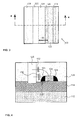
- FIGS. 1 and 2 schematically depict different design aspects of a part of a prior art semiconductor storage device
- FIGS. 3 and 4 schematically depict different design aspects of a part of a semiconductor storage device in accordance with an embodiment of the present disclosure
- FIG. 5 schematically depicts another view of a semiconductor storage device of FIG. 4 ;
- FIG. 6 schematically depicts a semiconductor storage device according to an embodiment that comprises multiple storage elements
- FIG. 7-9 schematically depict various views of parts of a semiconductor storage device in accordance with another embodiment.
- FIG. 10 schematically depicts a part of a semiconductor storage device in accordance with yet another embodiment.
- the present disclosure reflects a realization that in the design rules of most semiconductor technologies such as most CMOS processes, the minimum allowable space between a metal contact to a polysilicon line is smaller than the minimum allowable space between two polysilicon lines. For instance, in a 45 nm CMOS technology, the minimum allowable space between two polysilicon lines is defined at 100 nm whereas the minimum allowable space between a metal contact and a polysilicon line is 40 nm only. Similarly, in a 140 nm CMOS technology (CMOS14), the minimum allowable space between two polysilicon lines is 200 nm, whereas the minimum allowable space between a metal contact and a polysilicon line is only 120 nm.
- CMOS14 CMOS14
- a metal contact in the form of a metal contact line, which is sometimes referred to as a contact bar or a local interconnect line (LIL).
- LIL local interconnect line
- the minimum allowable space between a local interconnect line and a polysilicon line is comparable to the minimum allowable distance between a single contact and a polysilicon line; a typical example of such an allowable distance may be 120 nm in a 140 nm CMOS technology.
- FIG. 1 a top view of a part of a prior art semiconductor storage device 10 , a multiple-times programmable (MTP) non-volatile memory (NVM) cell, is shown.
- FIG. 2 shows a cross-section of the prior art semiconductor storage device 10 along the line 2 - 2 .
- the prior art semiconductor storage device 10 works as follows.
- a small polysilicon floating gate 22 is crossing an active line (not shown) formed in the semiconductor substrate 12 , which extends on to shallow trench insulation 14 .
- the active line typically comprises a channel region of a first conductivity type in between source and drain regions of an opposite conductivity type.
- the polysilicon floating gate 22 is typically arranged over the channel region and surrounded by nitride spacers 24 .
- a polysilicon control gate 26 which is also surrounded by nitride spaces 24 , is placed on shallow trench insulation 14 as close as possible to the floating gate 22 , i.e. at the minimum distance according to the design rules.
- the polysilicon control gate 26 surrounds the floating gate 22 as much as possible to maximize the capacitive coupling between these gate structures.
- the parallel run length between the control gate 26 and the floating gate 22 is chosen to be large enough to ensure that the capacitance formed by the control gate 26 , the floating gate 22 , and the oxide 28 in between these gates is about 10 times higher than the capacitance between the floating gate 22 and the semiconductor substrate 12 . This ensures that the memory for instance can be programmed by a Fowler-Nordheim tunneling mechanism.
- a high positive voltage may be applied to the control gate 26 with the substrate voltage maintained at 0V.
- the voltage of the floating gate 22 will rise to almost the control gate voltage; 10/11 ⁇ 0.9 of the control gate voltage. Consequently, a large voltage drop will be present across the tunnel oxide (not shown) of the floating gate 22 such that when the electric field is sufficiently large (roughly 10 MV/cm), electrons start to tunnel from the semiconductor substrate 12 to the floating gate 22 .
- V T threshold voltage
- Data erasing can be invoked in the same way by applying a negative voltage on the control gate 26 , thus causing electrons to tunnel back from the floating gate 22 to the semiconductor substrate 12 .
- FIG. 3 a top view of a part of a semiconductor storage device 100 in accordance with an embodiment of the present disclosure is shown.
- FIG. 4 shows a cross-section of a part of the semiconductor storage device 100 along the line 4 - 4 .
- a polysilicon floating gate 122 is crossing an active line (not shown) formed in the semiconductor substrate 112 , which extends on to shallow trench insulation 114 .
- the active line typically comprises a channel region of a first conductivity type in between source and drain regions of an opposite conductivity type.
- the active line, or at least the channel region is typically covered by a dielectric material such as a gate or tunnel oxide (not shown).
- the polysilicon floating gate 122 is typically arranged on top of this dielectric material over the channel region and surrounded by spacers 124 of a suitable material such as nitride and embedded in an electrically insulating material 128 , such as an oxide or another suitable insulating material.
- the spacers 124 are used for conventional CMOS process reasons such as the prevention of silicide bridge formation and the separation of light and heavily doped drain implants and are not essential.
- a metal control gate 126 for instance a tungsten control gate 126 , is also placed on the shallow trench insulation 114 as close as possible to the polysilicon floating gate 122 , i.e. at the minimum distance according to the design rules in the relevant semiconductor technology. Similar to the prior art device, the metal control gate 126 also surrounds the polysilicon floating gate 122 as much as possible to maximize the capacitive coupling between these gate structures.
- the distance 130 between the metal control gate 126 and the polysilicon floating gate 122 is significantly smaller than the minimum allowable distance 30 between the polysilicon control gate 26 and floating gate 22 in the prior art device 10 .
- the semiconductor storage device 100 further comprises fringe capacitances 132 ′ and 132 ′′ in addition to the lateral capacitance 132 formed by the metal control gate 126 , insulating material 128 , the spacer 124 and the polysilicon floating gate 122 , which further increases the capacitive coupling between these gate structures.
- the semiconductor storage device 100 compared to the prior art semiconductor storage device 10 will now be explained in more detail by means of an example semiconductor technology, for which a 140 nm CMOS process has been chosen.
- the minimum allowable distance between two polysilicon lines may for instance be chosen to be 200 nm, whereas the minimum allowable distance between a metal structure such as a LIL and a polysilicon line may be chosen to be 120 nm.
- these design rule values are given as non-limiting examples only since it will be apparent to the skilled person that such values may be varied within certain limits.
- the oxide layer 128 has a dielectric constant of ⁇ ox 4.2.
- This ratio may be further improved by ensuring that the height of the control gate 126 is much larger than the height of the polysilicon floating gate 122 such that the aforementioned fringe capacitance 132 ′ also contribute to the overall capacitance. Moreover, because in practice the metal control gate 126 will penetrate the shallow trench insulation 114 by at least a few tens of nm, an additional fringe capacitance 132 ′′ will further increase the overall capacitance of the storage cell of the semiconductor storage device 100 .
- the metal control gate 126 does not suffer from poly depletion issues that contribute to the EOT and has normally a detrimental effect on, i.e. Increases, the program or erase voltage of such a storage cell.
- a metal control gate 126 has a much lower sheet resistance, which improves the read-out speed of the semiconductor storage device 100 .
- FIG. 4 is a simplified representation of such a semiconductor storage device.
- additional structures such as additional dielectric layers located on top of the polysilicon floating gate 122 may be present without departing from the teachings of the present disclosure.
- the storage cell the semiconductor storage device 100 comprises a metal control gate 126 shaped as a metal contact bar or LIL as shown in FIG. 5 .
- the metal control gate 126 is shaped such that this gate partially surrounds the polysilicon floating gate 122 to maximize the capacitive coupling between these gates.
- FIG. 5 is an example of a 2-transistor (2T) cell according to an embodiment in which an access or selection transistor is placed next to the memory transistor and used as an enable device.
- FIG. 5 shows the polysilicon gate 150 of this access transistor.
- the first metal layer 160 which provides the interconnect structure to the respective contact pads 142 (to a source region), 144 (to a drain region), 146 (to the metal control gate 126 ) and 152 (to the polysilicon gate 150 of the access transistor) can be shaped to cover a large area of the floating gate 122 .
- the access transistor comprising the polysilicon gate 150 as well as the storage transistor comprising the polysilicon floating gate 126 is located in a single well 110 in the semiconductor substrate 112 .
- the semiconductor storage device 100 will comprise a plurality of such wells.
- the single well 110 may be an N-type well or a P-type well depending on the conductivity type of the storage transistor (and access transistor if present).
- the storage transistor (and access transistor if present) may be realized as a PMOS or as an NMOS transistor, amongst others.
- FIG. 5 gives a non-limiting example only of a possible storage cell layout, and many different layouts are suitable to achieve an improved capacitive coupling coefficient between the metal control gate 126 and the polysilicon floating gate 122 .
- FIG. 6 depicts a part of a semiconductor storage device in accordance with an embodiment in which a memory array comprising a storage cell 170 is shown, which comprises a comb-like or interdigitated metal control gate 126 and polysilicon floating gate 122 to maximize the capacitive coupling between these gates.
- FIG. 6 is a memory array in which the 2-T memory cells 170 , as is apparent from the presence of the polysilicon gate 150 of the access transistor, share a common source structure that is periodically connected by source contacts 142 .
- Such a configuration is commonly known as a NOR configuration. It is pointed out that alternative configurations, such as an AND configuration in which different rows of the memory array have their own source lines, are equally feasible.
- FIG. 7 a top view of a part of a semiconductor storage device 200 in accordance with another embodiment is shown.
- FIG. 8 shows a cross-section of a part of the semiconductor storage device 200 along the line 8 - 8
- FIG. 9 shows a cross-section of a part of the semiconductor storage device 200 along the line 9 - 9 .
- the continuous metal control gate structure 126 is replaced by a metal control gate structure formed by a row of multiple contacts 226 .
- each metal portion 226 is connected to the first metal layer 160 .
- FIG. 10 a cross-section of a part of a semiconductor storage device 300 in accordance with yet another embodiment is shown.
- a metal control gate structure 326 e.g. a metal LIL or contact bar, partially overlaps the spacer 124 that surrounds the polysilicon floating gate 122 .
- This embodiment is of particular relevance in advanced semiconductor technology generations such as a 45 nm CMOS process, in which the minimum allowable space between a metal contact and a polysilicon structure may be chosen to be as low as 40 nm, and wherein the width of the spacers 124 can easily exceed this distance.
- the capacitive coupling between the metal control gate structure 326 and the polysilicon floating gate 122 will be further improved, thanks to the fact that the dielectric medium between the metal control gate structure 326 and the polysilicon floating gate 122 is mainly formed by nitride materials which have a k-value of around 7.
- the semiconductor storage device of the various disclosed embodiments may be programmed in any suitable way, such as by Fowler-Nordheim tunnelling. This tunnelling principle is well-known to the skilled person and will not be further explained for reasons of brevity only. Alternative lower voltage programming and erasing methods such as Channel Hot Electron-injection and Punch-through Assisted Hot Hole Injection requiring the use of an additional MOS enable transistor for selecting the storage transistor to be programmed or erased are also feasible.
- a suitable method for manufacturing a semiconductor storage device in accordance with one of the aforementioned embodiments typically includes the steps of providing a semiconductor substrate having a first region of a first conductivity type in between respective regions of an opposite conductivity type, covering at least the first region with a first dielectric layer, forming a polysilicon floating gate on the first dielectric layer over the first region, embedding said floating gate in an insulating material; and forming a metal control gate structure adjacent to the polysilicon floating gate at a distance such that the metal control gate structure is capacitively coupled to the floating gate.
- the first conductivity type may be N-type or P-type with the opposite conductivity type being P-type or N-type respectively.
- the respective regions typically comprise a source region and a drain region, which may be formed by conventional implantation steps.
- the first dielectric layer e.g. a tunnel oxide layer, may be grown and patterned in any suitable way and the polysilicon floating gate 122 may be formed on top of this first dielectric layer using any suitable step such as the deposition and subsequent patterning of a polysilicon layer. Spacers may be grown around the gate in any suitable way and the resulting structure may be embedded in any suitable dielectric medium such as silicon oxide.
- the metal control gate structure for instance control gate structure 126 may be formed in any suitable way, e.g.
Landscapes
- Semiconductor Memories (AREA)
- Non-Volatile Memory (AREA)
Abstract
Description
C poly-poly=(∈ox h.L)/EOT poly-poly
where EOTpoly-poly is the equivalent oxide thickness with EOTpoly-poly=(2*60)* ∈ox/∈N+80=152 nm.
C metal-poly=(∈ox h.L)/EOT metal-poly
where EOTmetal-poly=(60)*∈ox/∈N+60=96 nm.
Claims (19)
Applications Claiming Priority (3)
| Application Number | Priority Date | Filing Date | Title |
|---|---|---|---|
| EP09160221 | 2009-05-14 | ||
| EP09160221.9A EP2251907B1 (en) | 2009-05-14 | 2009-05-14 | Semiconductor Storage Device and Manufacturing Method |
| EP09160221.9 | 2009-05-14 |
Publications (2)
| Publication Number | Publication Date |
|---|---|
| US20100308394A1 US20100308394A1 (en) | 2010-12-09 |
| US8334559B2 true US8334559B2 (en) | 2012-12-18 |
Family
ID=41076869
Family Applications (1)
| Application Number | Title | Priority Date | Filing Date |
|---|---|---|---|
| US12/780,612 Expired - Fee Related US8334559B2 (en) | 2009-05-14 | 2010-05-14 | Semiconductor storage device and manufacturing method |
Country Status (4)
| Country | Link |
|---|---|
| US (1) | US8334559B2 (en) |
| EP (1) | EP2251907B1 (en) |
| CN (1) | CN101901812A (en) |
| TW (1) | TWI405328B (en) |
Cited By (1)
| Publication number | Priority date | Publication date | Assignee | Title |
|---|---|---|---|---|
| US8772108B1 (en) * | 2013-02-25 | 2014-07-08 | Globalfoundries Singapore Pte. Ltd. | Multi-time programmable non-volatile memory |
Families Citing this family (5)
| Publication number | Priority date | Publication date | Assignee | Title |
|---|---|---|---|---|
| CN102709290B (en) * | 2012-05-22 | 2016-08-03 | 上海华虹宏力半导体制造有限公司 | Memorizer and forming method thereof |
| KR101978450B1 (en) * | 2012-12-21 | 2019-05-14 | 에스케이하이닉스 주식회사 | Nonvolatile memory device and method of fabricating the same |
| TWI608583B (en) * | 2016-12-14 | 2017-12-11 | 台灣半導體股份有限公司 | Common source package structure |
| TWI755943B (en) | 2020-11-23 | 2022-02-21 | 力晶積成電子製造股份有限公司 | Non-volatile memory device and method for manufacturing the same |
| CN119173036B (en) * | 2024-11-22 | 2025-03-11 | 合肥晶合集成电路股份有限公司 | A multi-time programmable device and electronic equipment |
Citations (5)
| Publication number | Priority date | Publication date | Assignee | Title |
|---|---|---|---|---|
| WO1990011621A1 (en) | 1989-03-27 | 1990-10-04 | Hughes Aircraft Company | Floating gate transistor and process for making it |
| US5394357A (en) | 1993-03-01 | 1995-02-28 | Yu; Shih-Chiang | Non-volatile semiconductor memory device |
| US20060176736A1 (en) | 2002-10-28 | 2006-08-10 | Eliyahou Harari | Flash Memory Cell Arrays Having Dual Control Gates Per Memory Cell Charge Storage Element |
| US7276759B1 (en) | 2004-03-11 | 2007-10-02 | Nanostar Corporation | Non-volatile electrically alterable semiconductor memory with control and floating gates and side-wall coupling |
| US20080291728A1 (en) | 2007-04-24 | 2008-11-27 | Esin Terzioglu | Single-Poly Non-Volatile Memory Cell |
Family Cites Families (6)
| Publication number | Priority date | Publication date | Assignee | Title |
|---|---|---|---|---|
| JP4222675B2 (en) * | 1999-03-29 | 2009-02-12 | 三洋電機株式会社 | Nonvolatile semiconductor memory device |
| KR100511598B1 (en) * | 2003-09-24 | 2005-08-31 | 동부아남반도체 주식회사 | Method of fabricating a flash memory |
| KR100688575B1 (en) * | 2004-10-08 | 2007-03-02 | 삼성전자주식회사 | Nonvolatile Semiconductor Memory Devices |
| US7176084B2 (en) * | 2005-06-09 | 2007-02-13 | Taiwan Semiconductor Manufacturing Co., Ltd. | Self-aligned conductive spacer process for sidewall control gate of high-speed random access memory |
| CN101236928A (en) * | 2007-01-30 | 2008-08-06 | 力晶半导体股份有限公司 | Method for manufacturing non-volatile memory |
| JP5106022B2 (en) * | 2007-09-28 | 2012-12-26 | ルネサスエレクトロニクス株式会社 | Nonvolatile semiconductor memory device and manufacturing method thereof |
-
2009
- 2009-05-14 EP EP09160221.9A patent/EP2251907B1/en active Active
-
2010
- 2010-05-14 CN CN2010101807927A patent/CN101901812A/en active Pending
- 2010-05-14 US US12/780,612 patent/US8334559B2/en not_active Expired - Fee Related
- 2010-05-14 TW TW099115410A patent/TWI405328B/en not_active IP Right Cessation
Patent Citations (5)
| Publication number | Priority date | Publication date | Assignee | Title |
|---|---|---|---|---|
| WO1990011621A1 (en) | 1989-03-27 | 1990-10-04 | Hughes Aircraft Company | Floating gate transistor and process for making it |
| US5394357A (en) | 1993-03-01 | 1995-02-28 | Yu; Shih-Chiang | Non-volatile semiconductor memory device |
| US20060176736A1 (en) | 2002-10-28 | 2006-08-10 | Eliyahou Harari | Flash Memory Cell Arrays Having Dual Control Gates Per Memory Cell Charge Storage Element |
| US7276759B1 (en) | 2004-03-11 | 2007-10-02 | Nanostar Corporation | Non-volatile electrically alterable semiconductor memory with control and floating gates and side-wall coupling |
| US20080291728A1 (en) | 2007-04-24 | 2008-11-27 | Esin Terzioglu | Single-Poly Non-Volatile Memory Cell |
Non-Patent Citations (1)
| Title |
|---|
| Search Report and Written Opinion dated Oct. 5, 2009 issued by the European Patent Office in European Application No. 09160221.9, 7 pages. |
Cited By (1)
| Publication number | Priority date | Publication date | Assignee | Title |
|---|---|---|---|---|
| US8772108B1 (en) * | 2013-02-25 | 2014-07-08 | Globalfoundries Singapore Pte. Ltd. | Multi-time programmable non-volatile memory |
Also Published As
| Publication number | Publication date |
|---|---|
| TWI405328B (en) | 2013-08-11 |
| EP2251907A1 (en) | 2010-11-17 |
| CN101901812A (en) | 2010-12-01 |
| EP2251907B1 (en) | 2015-12-02 |
| US20100308394A1 (en) | 2010-12-09 |
| TW201104844A (en) | 2011-02-01 |
Similar Documents
| Publication | Publication Date | Title |
|---|---|---|
| US8344443B2 (en) | Single poly NVM devices and arrays | |
| JP6092315B2 (en) | Highly scalable single poly nonvolatile memory cell | |
| US7889553B2 (en) | Single-poly non-volatile memory cell | |
| CN104517966B (en) | Single-layer polysilicon non-volatile memory unit | |
| JP2817500B2 (en) | Nonvolatile semiconductor memory device | |
| US20160260727A1 (en) | Nonvolatile memory cell structure with assistant gate and memory array thereof | |
| CN106952923B (en) | Non-volatile memory cell structure and array structure and manufacturing method | |
| US20100027347A1 (en) | Three-Terminal Single Poly NMOS Non-Volatile Memory Cell | |
| TW201426913A (en) | Non-volatile memory structure and its preparation method | |
| US8334559B2 (en) | Semiconductor storage device and manufacturing method | |
| US8587036B2 (en) | Non-volatile memory and fabricating method thereof | |
| JP3987247B2 (en) | Flash memory cell and manufacturing method thereof | |
| US7759720B2 (en) | Non-volatile semiconductor memory device and method of manufacturing the same | |
| US7531864B2 (en) | Nonvolatile memory device | |
| US8344440B2 (en) | Three-terminal single poly NMOS non-volatile memory cell with shorter program/erase times | |
| US10446568B2 (en) | Semiconductor memory and semiconductor memory manufacturing method | |
| US10388660B2 (en) | Semiconductor device and method for manufacturing the same | |
| US7633115B2 (en) | Electrically erasable programmable read only memory (EEPROM) cell | |
| US20070237004A1 (en) | Method of erasing an EEPROM device | |
| US8390052B2 (en) | Nonvolatile semiconductor memory device | |
| JPWO2009096083A1 (en) | Floating gate type nonvolatile memory device and manufacturing method thereof | |
| KR960014471B1 (en) | Nonvolatile semiconductor memory device and manufacturing method thereof | |
| CN120936030A (en) | Nonvolatile memory cell with single polysilicon floating gate and contact control gate | |
| TWI438869B (en) | Memory structure and fabricating method thereof | |
| US20060003516A1 (en) | Flash memory devices on silicon carbide |
Legal Events
| Date | Code | Title | Description |
|---|---|---|---|
| AS | Assignment |
Owner name: TAIWAN SEMICONDUCTOR MANUFACTURING COMPANY, LTD., Free format text: ASSIGNMENT OF ASSIGNORS INTEREST;ASSIGNORS:AKIL, NADER;VAN DUUREN, MICHIEL J.;SIGNING DATES FROM 20100728 TO 20100729;REEL/FRAME:024886/0021 |
|
| ZAAA | Notice of allowance and fees due |
Free format text: ORIGINAL CODE: NOA |
|
| ZAAB | Notice of allowance mailed |
Free format text: ORIGINAL CODE: MN/=. |
|
| STCF | Information on status: patent grant |
Free format text: PATENTED CASE |
|
| FPAY | Fee payment |
Year of fee payment: 4 |
|
| MAFP | Maintenance fee payment |
Free format text: PAYMENT OF MAINTENANCE FEE, 8TH YEAR, LARGE ENTITY (ORIGINAL EVENT CODE: M1552); ENTITY STATUS OF PATENT OWNER: LARGE ENTITY Year of fee payment: 8 |
|
| FEPP | Fee payment procedure |
Free format text: MAINTENANCE FEE REMINDER MAILED (ORIGINAL EVENT CODE: REM.); ENTITY STATUS OF PATENT OWNER: LARGE ENTITY |
|
| LAPS | Lapse for failure to pay maintenance fees |
Free format text: PATENT EXPIRED FOR FAILURE TO PAY MAINTENANCE FEES (ORIGINAL EVENT CODE: EXP.); ENTITY STATUS OF PATENT OWNER: LARGE ENTITY |
|
| STCH | Information on status: patent discontinuation |
Free format text: PATENT EXPIRED DUE TO NONPAYMENT OF MAINTENANCE FEES UNDER 37 CFR 1.362 |
|
| FP | Lapsed due to failure to pay maintenance fee |
Effective date: 20241218 |