US8330093B2 - Apparatus and method for preventing charge pumping in series connected diode stacks - Google Patents
Apparatus and method for preventing charge pumping in series connected diode stacks Download PDFInfo
- Publication number
- US8330093B2 US8330093B2 US12/692,874 US69287410A US8330093B2 US 8330093 B2 US8330093 B2 US 8330093B2 US 69287410 A US69287410 A US 69287410A US 8330093 B2 US8330093 B2 US 8330093B2
- Authority
- US
- United States
- Prior art keywords
- switch
- stack
- bias voltage
- diode stack
- diode
- Prior art date
- Legal status (The legal status is an assumption and is not a legal conclusion. Google has not performed a legal analysis and makes no representation as to the accuracy of the status listed.)
- Expired - Fee Related, expires
Links
- 238000000034 method Methods 0.000 title claims description 20
- 238000005086 pumping Methods 0.000 title claims description 15
- 230000000737 periodic effect Effects 0.000 claims description 12
- 230000007704 transition Effects 0.000 claims description 12
- 230000001052 transient effect Effects 0.000 claims description 11
- 230000005684 electric field Effects 0.000 claims description 8
- 230000000630 rising effect Effects 0.000 claims description 7
- 230000003068 static effect Effects 0.000 claims description 4
- 238000005259 measurement Methods 0.000 description 10
- 238000010586 diagram Methods 0.000 description 9
- 239000004973 liquid crystal related substance Substances 0.000 description 8
- 239000011521 glass Substances 0.000 description 7
- 238000005286 illumination Methods 0.000 description 6
- 230000008901 benefit Effects 0.000 description 4
- 239000000463 material Substances 0.000 description 4
- 230000005540 biological transmission Effects 0.000 description 3
- 230000001419 dependent effect Effects 0.000 description 3
- 238000004519 manufacturing process Methods 0.000 description 3
- 239000011159 matrix material Substances 0.000 description 3
- 230000003071 parasitic effect Effects 0.000 description 3
- 230000002441 reversible effect Effects 0.000 description 3
- 238000012935 Averaging Methods 0.000 description 2
- 230000000694 effects Effects 0.000 description 2
- 230000010354 integration Effects 0.000 description 2
- 238000012986 modification Methods 0.000 description 2
- 230000004048 modification Effects 0.000 description 2
- 230000008569 process Effects 0.000 description 2
- 239000010409 thin film Substances 0.000 description 2
- 230000009286 beneficial effect Effects 0.000 description 1
- 230000015556 catabolic process Effects 0.000 description 1
- 230000008878 coupling Effects 0.000 description 1
- 238000010168 coupling process Methods 0.000 description 1
- 238000005859 coupling reaction Methods 0.000 description 1
- 238000006731 degradation reaction Methods 0.000 description 1
- 230000001627 detrimental effect Effects 0.000 description 1
- 238000001914 filtration Methods 0.000 description 1
- 230000004313 glare Effects 0.000 description 1
- 230000007246 mechanism Effects 0.000 description 1
- 230000003287 optical effect Effects 0.000 description 1
- 229910021420 polycrystalline silicon Inorganic materials 0.000 description 1
- 230000009467 reduction Effects 0.000 description 1
- 239000000758 substrate Substances 0.000 description 1
Images


Classifications
-
- G—PHYSICS
- G01—MEASURING; TESTING
- G01J—MEASUREMENT OF INTENSITY, VELOCITY, SPECTRAL CONTENT, POLARISATION, PHASE OR PULSE CHARACTERISTICS OF INFRARED, VISIBLE OR ULTRAVIOLET LIGHT; COLORIMETRY; RADIATION PYROMETRY
- G01J1/00—Photometry, e.g. photographic exposure meter
- G01J1/42—Photometry, e.g. photographic exposure meter using electric radiation detectors
- G01J1/44—Electric circuits
-
- G—PHYSICS
- G01—MEASURING; TESTING
- G01J—MEASUREMENT OF INTENSITY, VELOCITY, SPECTRAL CONTENT, POLARISATION, PHASE OR PULSE CHARACTERISTICS OF INFRARED, VISIBLE OR ULTRAVIOLET LIGHT; COLORIMETRY; RADIATION PYROMETRY
- G01J1/00—Photometry, e.g. photographic exposure meter
- G01J1/10—Photometry, e.g. photographic exposure meter by comparison with reference light or electric value provisionally void
- G01J1/20—Photometry, e.g. photographic exposure meter by comparison with reference light or electric value provisionally void intensity of the measured or reference value being varied to equalise their effects at the detectors, e.g. by varying incidence angle
- G01J1/28—Photometry, e.g. photographic exposure meter by comparison with reference light or electric value provisionally void intensity of the measured or reference value being varied to equalise their effects at the detectors, e.g. by varying incidence angle using variation of intensity or distance of source
- G01J1/30—Photometry, e.g. photographic exposure meter by comparison with reference light or electric value provisionally void intensity of the measured or reference value being varied to equalise their effects at the detectors, e.g. by varying incidence angle using variation of intensity or distance of source using electric radiation detectors
- G01J1/32—Photometry, e.g. photographic exposure meter by comparison with reference light or electric value provisionally void intensity of the measured or reference value being varied to equalise their effects at the detectors, e.g. by varying incidence angle using variation of intensity or distance of source using electric radiation detectors adapted for automatic variation of the measured or reference value
-
- G—PHYSICS
- G01—MEASURING; TESTING
- G01J—MEASUREMENT OF INTENSITY, VELOCITY, SPECTRAL CONTENT, POLARISATION, PHASE OR PULSE CHARACTERISTICS OF INFRARED, VISIBLE OR ULTRAVIOLET LIGHT; COLORIMETRY; RADIATION PYROMETRY
- G01J1/00—Photometry, e.g. photographic exposure meter
- G01J1/42—Photometry, e.g. photographic exposure meter using electric radiation detectors
- G01J1/4204—Photometry, e.g. photographic exposure meter using electric radiation detectors with determination of ambient light
Definitions
- the present invention relates to light sensor circuits and, more particularly, to an apparatus and method for reducing average noise currents in series connected diode stacks of light sensor circuits used in display systems.
- FIG. 1 shows a simplified cross-section of a typical transmissive active-matrix liquid crystal display (AMLCD).
- the backlight 10 serves as a light source for illumination of the display.
- the transmission of light through the display, from the backlight 10 to the viewer 20 is controlled by the use of electronic circuits made from thin film transistors (TFTs).
- TFTs thin film transistors
- These TFTs are fabricated on a glass substrate (known as the TFT glass 30 ) and are operated in conjunction with a ‘counter-electrode’ 40 so as to vary the local electric field appearing across the liquid crystal (LC) layer 50 .
- the local electric field dictates the optical properties of the LC material, and thus permits selective transmission of light from the backlight 10 through to the viewer 20 .
- an electric field of non-zero mean is maintained over the LC material, it will suffer degradation.
- the transmission of light through the LC material is dictated by the magnitude of the applied field, rather than its polarity, it is acceptable to periodically invert the polarity of the field so as to achieve a zero mean.
- this inversion is accomplished by varying both the voltages present on the TFT glass 30 and that present on the common counter-electrode 40 .
- the counter-electrode 40 is typically driven with a square wave of several volts. The counter-electrode 40 signal may therefore act as a source of electrical interference to any other circuits integrated within the display.
- the signal supplied to the counter-electrode 40 is generated by electronics incorporated into the display module.
- An integrated circuit (IC) in the host product for example the mobile phone or portable computer which contains the display) generates further necessary display signals, such as HSYNC, CK and RGB. Examples of these signals can be found in FIG. 2 .
- An ambient light sensor is used for this purpose, and there are advantages to integrating the ALS onto the TFT glass 30 (termed ‘monolithic integration’). These advantages include reduction of the product's size, weight and manufacturing costs.
- a typical ambient light sensor system as shown in FIG. 3 , contains the following elements:
- the photodetection device used must be compatible with the TFT process employed in the manufacture of the TFT glass 30 .
- a well-known photodetection device compatible with the standard TFT process is the lateral thin-film poly-silicon P-I-N diode: a two terminal device having a cathode 100 and an anode 110 , whose circuit representation is shown in FIG. 4 .
- the current flowing in the P-I-N diode is a function of three quantities: temperature, the amount of illumination incident upon the diode, and the potential difference which appears across its terminals (the ‘bias voltage’).
- the asymmetric relationship between diode current (Iac) and applied bias voltage (Vac) is shown in FIG. 5 (for the case of zero illumination).
- the current which flows on account of a non-zero bias voltage is detrimental to the operation of an ambient light sensor, as it cannot be distinguished from that which flows due to incident illumination. This component of the diode current is termed the ‘dark current’, and may be significantly temperature dependent.
- FIG. 6 shows a series connected photodiode stack, as described in WO2008/044749A1, finding use in an ALS circuit.
- the stack of n series connected photodiodes 120 is connected to bias generating and current measurement circuitry 70 .
- the bias generating and current measurement circuitry 70 measures diode current whilst maintaining a constant (and ideally zero) bias voltage across the diode stack 120 .
- Any residual bias voltage, VB, appearing across the diode stack 120 is divided between the individual devices, such that each photodiode experiences a lesser bias of VB/n. Dark current from the photodiode is therefore reduced.
- series connected diodes have a disadvantage when employed within an electrically noisy environment.
- electrical interference from the counter-electrode 130 will couple to points within the diode stack 120 , via parasitic coupling capacitances 140 .
- the effect of electrical interference in sensor circuits may be reduced by techniques such as low pass filtering or averaging of the sensor output.
- the asymmetric conduction characteristic of the diode, shown in FIG. 5 may cause a net forward current to flow in the presence of electrical interference. This net forward current cannot be cancelled out by time-averaging or integration, and cannot be separated from the light dependent diode current.
- the cathode end diode 150 When an equally sized falling edge appears on the counter-electrode 130 , introducing negative voltage steps within the series connected diode stack 120 , the cathode end diode 150 will be reverse biased, and will pass little current. However, the anode end diode 160 will now be forward biased, and will allow a net forward current to pass into the stack 120 .
- capacitance may be present between nodes within the diode stack and ground (or other dc voltage sources). This is shown in FIG. 9 .
- the size of the voltage perturbations within the diode stack may vary along its length. Such uneven voltage perturbations may increase the transient forward bias voltages across diodes within the stack, raising the charge pumping current.
- the ‘charge pumping’ problem can be lessened by fabrication of a conductive shield layer 180 above the diode stack 120 . Electrically, this appears as shown in FIG. 10 . Although the conductive shield 180 is still capacitively coupled to the counter-electrode 130 , it is also grounded via a low resistance path 190 , minimizing the voltage perturbations which occur on it. The waveform appearing on the shield 180 may then resemble that shown in FIG. 11 . Only small voltage steps will therefore appear within the diode stack 120 on account of the counter-electrode waveform. As the current flowing in a forward biased diode is strongly dependent upon the magnitude of that forward bias voltage, smaller voltage perturbations within the stack 120 yield a lower charge pumping current. Nonetheless, it may not be possible to reduce the shield resistance to zero and hence the voltage perturbations sufficiently, and so the residual charge pumping current may still be unacceptable.
- the charge pumping problem can be eliminated by adoption of a display architecture whereby the counter-electrode voltage is constant.
- a display architecture whereby the counter-electrode voltage is constant.
- such architectures periodically invert the polarity of the voltages present on the TFT glass 30 , relative to that present on the counter-electrode 130 .
- higher absolute voltages must be generated on the TFT glass 30 of such displays, increasing complexity of the drive circuits.
- the bezel area (the non-display region which houses circuits surrounding the pixel matrix) may also be larger in displays of this architecture.
- the present invention provides an apparatus and method that reduces the average charge pumping current by periodically disconnecting the series connected diode stack from one or more of the bias voltages to which it is connected.
- This concept is shown in FIG. 12 , where an anode-end switch 210 and cathode-end switch 220 have been added to the series connected diode stack 120 . Disconnection of the diode stack is performed whenever interference sources cause transient internal voltages to be generated. Whilst disconnected from the bias source, transient voltages are generated uniformly at every point within the diode stack 120 , and equally at the endmost nodes 230 and 240 . For this reason no diode experiences a potential difference across its terminals, and no charge pumping current flows. Once the interference spike has passed, and voltages within the stack have returned to their original values, the stack may be reconnected to its bias source.
- the device and method in accordance with the present invention may also be applicable to cases where the diode stack is biased with a fixed forward current, and the resultant forward bias voltage is measured. Under these circumstances the charge pumping problem assists forward conduction through the stack, and so reduces the forward bias voltage measured under a given forward bias current.
- the apparatus and method in accordance with the present invention are able to suppress charge pumping without requiring adoption of an alternative display architecture, where the counter-electrode voltage remains static.
- an ambient light sensor includes: a first diode stack including at least two photodiodes, wherein a cathode of one of the at least two photodiodes is electrically connected to an anode of another of the at least two photodiodes; a bias source for providing a bias voltage to the first diode stack; and at least one switch electrically connected to the first stack, said at least one switch operative to selectively apply the bias voltage to and remove the bias voltage from the first diode stack.
- the at least one switch comprises a first switch and a second switch, and wherein the first switch is electrically connected between an end-most anode of the first diode stack and signal common, and the second switch is electrically connected between an end-most cathode of the first diode stack and the bias source.
- the ALS further includes at least one additional diode stack including at least two photodiodes, wherein a cathode of one of the at least two photodiodes is electrically coupled to an anode of another of the at least two photodiodes, and wherein the first diode stack and the at least one additional diode stack are electrically connected to one another in a series connection.
- the at least one switch comprises a plurality of switches, and one of the plurality of switches electrically couples the first stack to the at least one additional stack.
- the at least one switch comprises a plurality of switches, and one of the plurality of switches electrically couples the cathode of the one photodiode of the first stack to the anode of the another photodiode of the first stack.
- another of the plurality of switches electrically couples the cathode of the one photodiode of the additional diode stack to the anode of the another photodiode of the additional diode stack.
- the at least one switch comprises at least one of an n-channel transistor or a p-channel transistor.
- the ALS further includes a controller for controlling an open and closed state of the at least one switch.
- a display module includes: the ALS as set forth herein; and a counter-electrode for varying a local electric field, the counter-electrode capacitively coupled to the first stack and subjected to a first electrical waveform, wherein the controller is configured to open and close the at least one switch to correspond with transitions in the first electrical waveform.
- the controller is configured to open and close the at least one switch to correspond with a period of the first electrical waveform.
- the controller is configured to close the at least one switch during high or low half cycles of the first electrical waveform.
- the controller is configured to close the at least one switch once every second high pulse or every second low pulse of the first electrical waveform.
- the controller is configured to open the at least one switch during at least one of rising or falling edges of the first electrical waveform.
- the display module further includes a shield layer capacitively coupled to the first stack, said shield layer subjected to a second electrical waveform different from the first electrical waveform, wherein the controller is configured to close the at least one switch following each transition of the first electrical waveform.
- the second waveform is derived from the first waveform.
- the display module further includes a shield layer capacitively coupled to the first stack, said shield layer subjected to a second electrical waveform different from the first electrical waveform, wherein the controller is configured to close the at least one switch following each second transition of the first electrical waveform.
- the controller is configured to open the at least one switch before a new transition of the first electrical waveform.
- the at least one switch is electrically connected between an end-most cathode of the first diode stack and the bias source, and wherein the controller is configured to open the at least one switch every low half cycle of the first electrical waveform.
- the at least one switch is electrically connected between an end-most anode of the first diode stack and signal common, and wherein the controller opens the at least one switch every high half cycle of the first electrical waveform.
- the controller is configured to close the at least one switch only when the first electrical waveform is static.
- the display module further includes a backlight.
- a method for preventing charge pumping in a series connected diode stack of a display device's ambient light sensor is provided, wherein the diode stack includes at least two photodiodes, and a cathode of one of the at least two photodiodes is electrically connected to an anode of another of the at least two photodiodes, the ALS including a bias source for generating a bias voltage for the diode stack, and the display device including a counter electrode for generating an electric field.
- the method includes selectively applying the bias voltage to and removing the bias voltage from the diode stack based on transient voltages on the counter electrode.
- selectively applying the bias voltage to and removing the bias voltage from the diode stack includes using a switch to apply the bias voltage to and remove the bias voltage from the diode stack.
- selectively applying the bias voltage to and removing the bias voltage from the diode stack includes applying and removing the bias voltage based on a periodic waveform applied to the counter-electrode.
- selectively removing the bias voltage includes removing the bias voltage from the stack with each rising or falling edge of the periodic waveform.
- selectively removing the bias voltage includes removing the bias voltage every second high or low pulse of the periodic waveform.
- the at least one switch is electrically connected between an end-most cathode of the diode stack and the bias source, and wherein selectively removing the bias voltage includes opening the at least one switch on a low pulse of the periodic waveform.
- the at least one switch is electrically connected between an end-most anode of the diode stack and signal common, and wherein selectively removing the bias voltage includes opening the at least one switch on a high pulse of the periodic waveform.
- the display device includes a shield layer capacitively coupled to the diode stack, and wherein selectively applying the bias voltage to the diode stack includes applying the bias voltage following each transient on the counter electrode.
- FIG. 1 is a cross section of a typical transmissive active matrix liquid crystal display (AMLCD).
- AMLCD transmissive active matrix liquid crystal display
- FIG. 2 illustrates exemplary display signals that may be used in a display system.
- FIG. 3 is a schematic diagram representing a simple ALS, built around an integrator and employing a single photodiode as a photosensitive element.
- FIG. 4 is the circuit symbol used for a photodiode.
- FIG. 5 is a graph showing a simplified current vs. voltage characteristic for a photodiode, when no light is present.
- FIG. 6 is a schematic diagram showing an ALS of the type depicted by FIG. 3 , yet which employs a stack of series connected photodiodes.
- FIG. 7 is a schematic diagram showing the mechanism by which electrical interference couples to nodes within the series connected diode stack.
- FIG. 8 is a schematic diagram illustrating how the endmost diodes of FIG. 7 become forward biased in the presence of electrical interference.
- FIG. 9 is a schematic diagram illustrating how capacitance may also exist between the diode stack and ground (or another DC voltage).
- FIG. 10 is a schematic diagram showing how a grounded shield may be used to minimize the electrical interference which couples to the stack of series connected photodiodes.
- FIG. 11 is a graph showing the voltage waveforms which may be expected to arise on the counter-electrode and the shield.
- FIG. 12 is a schematic diagram which shows periodic disconnection of the series connected photodiodes from the bias generating and current measurement circuitry in accordance with an embodiment of the present invention.
- FIG. 13 is a graph showing the variation of the counter-electrode voltage with time, together with a proposed timing for the switches in accordance with an embodiment of the invention.
- FIG. 14 is a graph showing the variation of the counter-electrode voltage with time, together with a proposed timing for the switches in accordance with an embodiment of the invention.
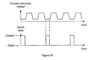
- FIG. 15 is a graph showing the variation of the counter-electrode voltage with time, together with an alternative timing for the switches in accordance with an embodiment of the invention.
- FIG. 16 is a graph showing the variation of the counter-electrode voltage with time, together with a corresponding variation in the shield voltage with time, and a proposed timing for the switches in accordance with an embodiment of the invention.
- FIG. 17 is a graph showing the variation of the counter-electrode voltage with time, together with a corresponding variation in the shield voltage with time, and an alternative timing for the switches in accordance with an embodiment of the invention.
- FIG. 18 is a schematic showing a diode stacks connected to a single switch.
- the diode stack is permanently connected to the bias generation and current measurement circuitry in accordance with an embodiment of the invention.
- FIG. 19 is a schematic showing a diode stack connected to a single switch, wherein the diode stack is permanently connected to ground in accordance with an embodiment of the invention.
- FIG. 20 shows two diode stacks, separated by a switch, and having switches at each end, wherein one terminal of one endmost switch is connected to the bias circuitry, whilst one terminal of the other endmost switch is connected to ground in accordance with an embodiment of the invention.
- FIG. 21 is a schematic diagram which shows a switch within the diode stack in accordance with an embodiment of the present invention.
- FIG. 12 is a schematic diagram showing a stack 120 of at least two series connected photodiodes, arranged such that the cathode of one is connected to the anode of the next.
- the end-most anode 230 is connected to one terminal of a simple two terminal switch 210 , the other terminal of this switch being connected to ground.
- the end-most cathode 240 is connected to one terminal of a second two terminal switch 220 , the other end of this switch being connected to terminal ‘A’ of bias and current measurement circuitry 245 .
- This bias generating and current measurement circuitry 245 is embodied in the form of an integrator 70 as shown in FIG. 3 , and described in WO2008/044749A1.
- the switches 210 and 220 are controlled via a controller 225 , which commands the switches to open and close using known techniques.
- the controller 225 is operatively coupled to the counter-electrode 130 and/or shield layer 180 , and commands the switches based on the electrical waveforms present on the counter-electrode and/or shield layer.
- the switches 210 and 220 may be implemented as either n-channel transistors, p-channel transistors, or an appropriate combination of the two.
- the switches 210 and 220 are operated as shown in FIG.
- FIG. 13 shows the counter-electrode voltage rising and falling as a periodic square wave, having finite rise and fall time.
- the switches are closed during one half-period of each cycle of the counter-electrode waveform, and are open during rising or falling edges of the counter-electrode waveform.
- the switches are closed when voltages developed within the series connected diode stack 120 are sufficiently small (i.e., small enough to reduce the average noise current to an acceptable level for the sensor circuit). This will be the case as soon as the counter-electrode signal has settled to its new value.
- FIG. 13 shows the switches being closed during the low half-cycle of the counter-electrode voltage, they may instead be closed during the high half-cycle.
- the signals required to drive switch 210 and switch 220 may easily be generated by the controller IC in the display module which generates the V COM signal. The manner in which these signals may be generated will be evident to those skilled in the art.
- FIGS. 12 and 15 show a device in accordance with a second embodiment of the invention, whereby the switches 210 and 220 are operated as shown in FIG. 15 .
- the switches close only when the counter-electrode voltage is static, as was shown in FIG. 13 .
- the switches close once every second low pulse or once every second high pulse of the counter-electrode waveform, rather than once every period. This may be advantageous, as it reduces the rate at which the switches are being operated and hence reduces the frequency of noise which couples from the switch signals themselves to other parts of the circuitry (such as to the bias generation and current measurement circuitry 245 ).
- FIGS. 12 and 16 show a device in accordance with a third and preferred embodiment of the invention, whereby switches 210 and 220 are operated in the manner shown in FIG. 16 .
- the third embodiment is used when a shield layer 180 is present above the diode stack 120 .
- FIG. 16 shows that the switches are closed following each transition of the counter-electrode voltage and once the voltage upon the conductive shield layer has settled. A short delay is utilized between each transition ending and the switches being closed, allowing time for transient voltages within the diode stack to decay to levels which will not produce a significant charge pumping current.
- the switches are opened before a new transition of the counter-electrode voltage occurs, as this will be accompanied by transient voltages within the stack.
- This embodiment is preferred because the switches may be opened more frequently than other embodiments. This is beneficial when the diode stack current must be determined within a short time.
- FIGS. 12 and 17 show a device in accordance with a fourth embodiment of the invention, applicable in cases where a conductive shield layer is fabricated above the diode stack, as previously described.
- FIG. 17 shows that switches 210 and 220 are operated following decay of transient voltage present within the diode stack 120 , in a manner similar to that previously shown in FIG. 16 .
- the switches are only closed once every two transitions of the counter-electrode voltage. This may be advantageous, as it reduces the rate at which the switches are being operated and hence reduces the frequency of noise which couples from the switch signals themselves to other parts of the circuitry (such as to the bias generation and current measurement circuitry 245 ).
- FIGS. 18 and 13 show a device in accordance with a fifth embodiment of the invention, whereby only one switch 280 is employed, and this switch is connected between the bias circuitry and the cathode end of the series connected diode stack 285 .
- the switch 280 is operated according to FIG. 13 .
- This embodiment is advantageous in that fewer components are required, relative to the first embodiment.
- the switch is now opened only on the low half-cycle of the counter-electrode voltage, and not on the high half-cycle. This ensures that only positive voltages are developed within the diode stack 285 , ensuring that the diode 288 at the anode end of the stack is never forward biased even though its anode is permanently connected to ground.
- FIGS. 19 and 14 show a device in accordance with a sixth embodiment of the invention, whereby only one switch 290 is employed, and this switch is connected between ground and the anode end of the series connected diode stack 295 .
- the switch 290 is operated as shown in FIG. 14 .
- This embodiment is advantageous in that fewer components are required, relative to the first embodiment.
- the switch is opened only on the high half-cycle of the counter-electrode voltage, and not on the low half-cycle. This ensures that only negative voltages are developed within the diode stack 295 , ensuring that the diode 298 at the cathode end of the stack is never forward biased even though its cathode is permanently connected to the dc bias voltage.
- FIG. 20 shows a device in accordance with a seventh embodiment of the invention, in which two series connected diode stacks 300 and 310 , of the kind previously described, are connected in series yet separated by a switch 320 .
- the stacks are connected such that the anode end of stack 300 is connected to one terminal of the switch 320 , the other terminal of the switch 320 being connected to the cathode of the remaining stack 310 .
- the anode of the stack 310 is connected to the first terminal of a switch 330 , whose second terminal is connected to ground.
- the cathode of the stack 300 is connected to the first terminal of a switch 340 , whose second terminal is connected to the bias circuitry.
- switches within the diode stack By including switches within the diode stack, charge pumping is further reduced in the case when unequal transient voltage perturbations are generated throughout the stack.
- the switches When the stack has a conductive shield layer, the switches may be operated as shown in FIGS. 16 and 17 .
- the switches When the stack does not have a conductive shield layer, the switches may be operated as shown in FIG. 13 , 14 or 15 .
- FIG. 21 shows a device in accordance with an eighth embodiment of the invention.
- the embodiment of FIG. 21 is similar to the embodiment shown in FIG. 12 , except that the diode stack 350 includes at least one switch 360 electrically coupled between two photodiodes of the stack.
- the switches When the stack has a conductive shield layer, the switches may be operated as shown in FIGS. 16 and 17 . When the stack does not have a conductive shield layer, the switches may be operated as shown in FIG. 13 , 14 or 15 .
- FIG. 21 shows switches at the ends of the stack and within the stack, it is possible that switches be provided only within the stack (between photodiodes of the stack). In such configuration, the ends of the stack may be directly coupled to the bias source.
- the anode end of the series connected diode stack shown connected to ground, may equally be connected to a dc voltage source.
Landscapes
- Physics & Mathematics (AREA)
- General Physics & Mathematics (AREA)
- Spectroscopy & Molecular Physics (AREA)
- Life Sciences & Earth Sciences (AREA)
- Sustainable Development (AREA)
- Control Of Indicators Other Than Cathode Ray Tubes (AREA)
- Liquid Crystal Display Device Control (AREA)
Abstract
Description
-
- (a) A photodetection element (or elements) capable of converting incoming light to electrical current. An example of such a photodetection element is a
photodiode 60. - (b) Voltage bias generating and current measurement circuitry to control the photodetection element(s) and sense the photo-generated
current 70. This circuitry will typically take the form of an integrator. - (c)
Output circuitry 80 to supply an output signal (analog or digital) representing the measured ambient light level. - (d) A means of adjusting the
display operation 90 based on the measured ambient light level, for example by controlling the intensity of thebacklight 10.
The operation of such components is described in WO2008/044749A1.
- (a) A photodetection element (or elements) capable of converting incoming light to electrical current. An example of such a photodetection element is a
Claims (29)
Priority Applications (3)
| Application Number | Priority Date | Filing Date | Title |
|---|---|---|---|
| US12/692,874 US8330093B2 (en) | 2009-11-17 | 2010-01-25 | Apparatus and method for preventing charge pumping in series connected diode stacks |
| PCT/JP2010/070636 WO2011062246A1 (en) | 2009-11-17 | 2010-11-12 | Ambient light sensor, display module and method for preventing charge pumping in series connected diode stacks |
| CN201080051598.7A CN102668129B (en) | 2009-11-17 | 2010-11-12 | Ambient light sensor, display module and method for preventing charge pumping in series connected diode stacks |
Applications Claiming Priority (2)
| Application Number | Priority Date | Filing Date | Title |
|---|---|---|---|
| US26188009P | 2009-11-17 | 2009-11-17 | |
| US12/692,874 US8330093B2 (en) | 2009-11-17 | 2010-01-25 | Apparatus and method for preventing charge pumping in series connected diode stacks |
Publications (2)
| Publication Number | Publication Date |
|---|---|
| US20110114824A1 US20110114824A1 (en) | 2011-05-19 |
| US8330093B2 true US8330093B2 (en) | 2012-12-11 |
Family
ID=44010605
Family Applications (1)
| Application Number | Title | Priority Date | Filing Date |
|---|---|---|---|
| US12/692,874 Expired - Fee Related US8330093B2 (en) | 2009-11-17 | 2010-01-25 | Apparatus and method for preventing charge pumping in series connected diode stacks |
Country Status (3)
| Country | Link |
|---|---|
| US (1) | US8330093B2 (en) |
| CN (1) | CN102668129B (en) |
| WO (1) | WO2011062246A1 (en) |
Families Citing this family (2)
| Publication number | Priority date | Publication date | Assignee | Title |
|---|---|---|---|---|
| CN110752838B (en) * | 2019-11-11 | 2023-10-31 | 上海联影医疗科技股份有限公司 | series diode circuit |
| EP3839930A1 (en) * | 2019-12-19 | 2021-06-23 | STMicroelectronics (Research & Development) Limited | Method and device for ambient light measurement |
Citations (7)
| Publication number | Priority date | Publication date | Assignee | Title |
|---|---|---|---|---|
| US5323068A (en) * | 1992-11-17 | 1994-06-21 | National Semiconductor Corporation | Low power low temperature ECL output driver circuit |
| US20020070790A1 (en) * | 2000-12-12 | 2002-06-13 | Westerman Stephen J. | Expandable multiport transfer switch |
| US20050122138A1 (en) * | 2003-12-09 | 2005-06-09 | Intel Corporation | Power supplies noise detector for integrated circuits |
| US20050258341A1 (en) | 2004-05-21 | 2005-11-24 | Sanyo Electric Co., Ltd. | Light quantity detection circuit and display panel using the same |
| WO2008044749A1 (en) | 2006-10-04 | 2008-04-17 | Sharp Kabushiki Kaisha | Photosensor and ambient light sensor |
| US20080290259A1 (en) | 2005-05-27 | 2008-11-27 | Alan Mathewson | Photon Counting Apparatus |
| US20110043284A1 (en) * | 2009-08-19 | 2011-02-24 | Qualcomm Incorporated | Stacked amplifier with diode-based biasing |
Family Cites Families (7)
| Publication number | Priority date | Publication date | Assignee | Title |
|---|---|---|---|---|
| JP2004357158A (en) * | 2003-05-30 | 2004-12-16 | Toshiba Corp | Optical receiver |
| JP2005283279A (en) * | 2004-03-29 | 2005-10-13 | Victor Co Of Japan Ltd | Photoelectric conversion circuit |
| CN1699936A (en) * | 2004-05-21 | 2005-11-23 | 三洋电机株式会社 | Light quantity detection circuit and display panel using the same |
| JP4192880B2 (en) * | 2004-10-12 | 2008-12-10 | セイコーエプソン株式会社 | Electro-optical device and electronic apparatus |
| WO2007013534A1 (en) * | 2005-07-27 | 2007-02-01 | Semiconductor Energy Laboratory Co., Ltd. | Semiconductor device |
| KR100824855B1 (en) * | 2006-12-27 | 2008-04-23 | 삼성에스디아이 주식회사 | Ambient light sensing circuit and flat panel display device having the same |
| JP5305387B2 (en) * | 2007-12-25 | 2013-10-02 | セイコーインスツル株式会社 | Photodetection device and image display device |
-
2010
- 2010-01-25 US US12/692,874 patent/US8330093B2/en not_active Expired - Fee Related
- 2010-11-12 CN CN201080051598.7A patent/CN102668129B/en not_active Expired - Fee Related
- 2010-11-12 WO PCT/JP2010/070636 patent/WO2011062246A1/en not_active Ceased
Patent Citations (11)
| Publication number | Priority date | Publication date | Assignee | Title |
|---|---|---|---|---|
| US5323068A (en) * | 1992-11-17 | 1994-06-21 | National Semiconductor Corporation | Low power low temperature ECL output driver circuit |
| US20020070790A1 (en) * | 2000-12-12 | 2002-06-13 | Westerman Stephen J. | Expandable multiport transfer switch |
| US6867635B2 (en) * | 2000-12-12 | 2005-03-15 | Agilent Technologies, Inc. | Expandable multiport transfer switch |
| US20050122138A1 (en) * | 2003-12-09 | 2005-06-09 | Intel Corporation | Power supplies noise detector for integrated circuits |
| US7157947B2 (en) * | 2003-12-09 | 2007-01-02 | Intel Corporation | Power supplies noise detector for integrated circuits |
| US20050258341A1 (en) | 2004-05-21 | 2005-11-24 | Sanyo Electric Co., Ltd. | Light quantity detection circuit and display panel using the same |
| JP2006013407A (en) | 2004-05-21 | 2006-01-12 | Sanyo Electric Co Ltd | Light amount detection circuit and display panel using the same |
| US20080290259A1 (en) | 2005-05-27 | 2008-11-27 | Alan Mathewson | Photon Counting Apparatus |
| JP2008542706A (en) | 2005-05-27 | 2008-11-27 | センスル・テクノロジーズ・リミテッド | Photon counting device |
| WO2008044749A1 (en) | 2006-10-04 | 2008-04-17 | Sharp Kabushiki Kaisha | Photosensor and ambient light sensor |
| US20110043284A1 (en) * | 2009-08-19 | 2011-02-24 | Qualcomm Incorporated | Stacked amplifier with diode-based biasing |
Non-Patent Citations (1)
| Title |
|---|
| International Search Report for corresponding International Application No. PCT/JP2010/070636 mailed Mar. 1, 2011. |
Also Published As
| Publication number | Publication date |
|---|---|
| US20110114824A1 (en) | 2011-05-19 |
| WO2011062246A1 (en) | 2011-05-26 |
| CN102668129A (en) | 2012-09-12 |
| CN102668129B (en) | 2015-02-25 |
Similar Documents
| Publication | Publication Date | Title |
|---|---|---|
| CN101680803B (en) | Optical sensor and display device provided with the same | |
| KR100997977B1 (en) | Optical sensor and display device using same | |
| CN101256296B (en) | Semiconductor device, display device, and electronic equipment having same | |
| US10198990B2 (en) | Device for temperature detection and device for compensating for temperature of display panel | |
| CN101600985B (en) | Display device | |
| CN101611499B (en) | Display device | |
| CN101611340B (en) | Display device | |
| JP4868425B2 (en) | Display device, electronic apparatus having the same, and optical sensor device | |
| JP2007279093A (en) | Liquid crystal display | |
| US7414601B2 (en) | Driving circuit for liquid crystal display device and method of driving the same | |
| CN101615384B (en) | Liquid crystal display | |
| US8330093B2 (en) | Apparatus and method for preventing charge pumping in series connected diode stacks | |
| JP2007205902A (en) | Light detecting circuit, electro-optical device, and electronic equipment | |
| KR100996573B1 (en) | Analog buffer and its driving method | |
| US7928972B2 (en) | Display device | |
| CN112967654A (en) | GIP circuit and driving method | |
| JP2007140106A (en) | Display apparatus | |
| US20090289915A1 (en) | Display device with optical sensors | |
| KR20100006022A (en) | Liquid crystal display device and method for driving the same | |
| JP2008026688A (en) | Display device | |
| JP2011128628A (en) | Display device | |
| KR101428634B1 (en) | Sensor circuit and driving circuit for LCD backlight and driving method thereof | |
| JP2008209556A (en) | Electro-optical device, semiconductor device, display device and electronic equipment having the same | |
| KR20050034768A (en) | Scan voltage generation apparatus and liquid crystal display using the same | |
| JP2007114260A (en) | Liquid crystal display |
Legal Events
| Date | Code | Title | Description |
|---|---|---|---|
| AS | Assignment |
Owner name: SHARP KABUSHIKI KAISHA, JAPAN Free format text: ASSIGNMENT OF ASSIGNORS INTEREST;ASSIGNORS:COULSON, MICHAEL P.;WASHIO, HAJIME;HADWEN, BENJAMIN J.;AND OTHERS;SIGNING DATES FROM 20091023 TO 20091126;REEL/FRAME:023889/0955 |
|
| ZAAA | Notice of allowance and fees due |
Free format text: ORIGINAL CODE: NOA |
|
| ZAAB | Notice of allowance mailed |
Free format text: ORIGINAL CODE: MN/=. |
|
| STCF | Information on status: patent grant |
Free format text: PATENTED CASE |
|
| FEPP | Fee payment procedure |
Free format text: PAYOR NUMBER ASSIGNED (ORIGINAL EVENT CODE: ASPN); ENTITY STATUS OF PATENT OWNER: LARGE ENTITY |
|
| FPAY | Fee payment |
Year of fee payment: 4 |
|
| MAFP | Maintenance fee payment |
Free format text: PAYMENT OF MAINTENANCE FEE, 8TH YEAR, LARGE ENTITY (ORIGINAL EVENT CODE: M1552); ENTITY STATUS OF PATENT OWNER: LARGE ENTITY Year of fee payment: 8 |
|
| FEPP | Fee payment procedure |
Free format text: MAINTENANCE FEE REMINDER MAILED (ORIGINAL EVENT CODE: REM.); ENTITY STATUS OF PATENT OWNER: LARGE ENTITY |
|
| LAPS | Lapse for failure to pay maintenance fees |
Free format text: PATENT EXPIRED FOR FAILURE TO PAY MAINTENANCE FEES (ORIGINAL EVENT CODE: EXP.); ENTITY STATUS OF PATENT OWNER: LARGE ENTITY |
|
| STCH | Information on status: patent discontinuation |
Free format text: PATENT EXPIRED DUE TO NONPAYMENT OF MAINTENANCE FEES UNDER 37 CFR 1.362 |
|
| FP | Lapsed due to failure to pay maintenance fee |
Effective date: 20241211 |