US8324648B2 - Semiconductor light emitting device package - Google Patents
Semiconductor light emitting device package Download PDFInfo
- Publication number
- US8324648B2 US8324648B2 US12/939,180 US93918010A US8324648B2 US 8324648 B2 US8324648 B2 US 8324648B2 US 93918010 A US93918010 A US 93918010A US 8324648 B2 US8324648 B2 US 8324648B2
- Authority
- US
- United States
- Prior art keywords
- light emitting
- emitting device
- semiconductor light
- reflective
- nanometer
- Prior art date
- Legal status (The legal status is an assumption and is not a legal conclusion. Google has not performed a legal analysis and makes no representation as to the accuracy of the status listed.)
- Expired - Fee Related, expires
Links
Images


Classifications
-
- H—ELECTRICITY
- H10—SEMICONDUCTOR DEVICES; ELECTRIC SOLID-STATE DEVICES NOT OTHERWISE PROVIDED FOR
- H10H—INORGANIC LIGHT-EMITTING SEMICONDUCTOR DEVICES HAVING POTENTIAL BARRIERS
- H10H20/00—Individual inorganic light-emitting semiconductor devices having potential barriers, e.g. light-emitting diodes [LED]
- H10H20/80—Constructional details
- H10H20/85—Packages
- H10H20/855—Optical field-shaping means, e.g. lenses
- H10H20/856—Reflecting means
-
- H—ELECTRICITY
- H10—SEMICONDUCTOR DEVICES; ELECTRIC SOLID-STATE DEVICES NOT OTHERWISE PROVIDED FOR
- H10H—INORGANIC LIGHT-EMITTING SEMICONDUCTOR DEVICES HAVING POTENTIAL BARRIERS
- H10H20/00—Individual inorganic light-emitting semiconductor devices having potential barriers, e.g. light-emitting diodes [LED]
- H10H20/80—Constructional details
- H10H20/85—Packages
- H10H20/855—Optical field-shaping means, e.g. lenses
-
- H—ELECTRICITY
- H10—SEMICONDUCTOR DEVICES; ELECTRIC SOLID-STATE DEVICES NOT OTHERWISE PROVIDED FOR
- H10H—INORGANIC LIGHT-EMITTING SEMICONDUCTOR DEVICES HAVING POTENTIAL BARRIERS
- H10H20/00—Individual inorganic light-emitting semiconductor devices having potential barriers, e.g. light-emitting diodes [LED]
- H10H20/80—Constructional details
- H10H20/84—Coatings, e.g. passivation layers or antireflective coatings
- H10H20/841—Reflective coatings, e.g. dielectric Bragg reflectors
-
- H—ELECTRICITY
- H10—SEMICONDUCTOR DEVICES; ELECTRIC SOLID-STATE DEVICES NOT OTHERWISE PROVIDED FOR
- H10H—INORGANIC LIGHT-EMITTING SEMICONDUCTOR DEVICES HAVING POTENTIAL BARRIERS
- H10H20/00—Individual inorganic light-emitting semiconductor devices having potential barriers, e.g. light-emitting diodes [LED]
- H10H20/80—Constructional details
- H10H20/882—Scattering means
-
- H—ELECTRICITY
- H10—SEMICONDUCTOR DEVICES; ELECTRIC SOLID-STATE DEVICES NOT OTHERWISE PROVIDED FOR
- H10W—GENERIC PACKAGES, INTERCONNECTIONS, CONNECTORS OR OTHER CONSTRUCTIONAL DETAILS OF DEVICES COVERED BY CLASS H10
- H10W90/00—Package configurations
- H10W90/701—Package configurations characterised by the relative positions of pads or connectors relative to package parts
- H10W90/751—Package configurations characterised by the relative positions of pads or connectors relative to package parts of bond wires
- H10W90/756—Package configurations characterised by the relative positions of pads or connectors relative to package parts of bond wires between a chip and a stacked lead frame, conducting package substrate or heat sink
Definitions
- the disclosure relates generally to semiconductor technology, and more particularly to a semiconductor light emitting device package.
- LEDs light emitting diodes
- OLEDs organic light emitting diodes
- LDs laser diodes
- Semiconductor light emitting device packages provide a reflector to accommodate the light field of the semiconductor light emitting devices.
- the reflector is polyphthalamide (PPA) or polypropylene (PP), having limited reflection due to luminous absorption that results in light extraction reduction. What is needed, therefore, is a semiconductor light emitting device package which can overcome the described limitations.
- FIG. 1 is a cross section of a semiconductor light emitting device package in accordance with a first embodiment of the disclosure.
- FIG. 2 is an enlarged view of a circled portion II of FIG. 1 , showing a cross section of a plurality of first reflective nanometer-structures of the semiconductor light emitting device package of FIG. 1 .
- FIG. 3 is a top view of the semiconductor light emitting device package in accordance with the first embodiment of FIG. 1 .
- FIGS. 4A to 4F are cross sections of a plurality of first nanometer-reflective structures with modified structures.
- FIG. 5 is a cross section of a semiconductor light emitting device package in accordance with a second embodiment of the disclosure.
- FIG. 6 is an enlarged view of a circled portion VI of FIG. 5 , showing a cross section of a plurality of second reflective nanometer-structures of the semiconductor light emitting device package of FIG. 5 .
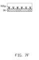
- FIGS. 7A to 7F are cross sections of a plurality of second nanometer-reflective structures with modified structures.
- the disclosure provides a first embodiment of a semiconductor light emitting device package 1 , comprising a semiconductor light emitting device 10 , a lead frame 20 and a reflector 30 .
- the lead frame 20 comprises a carrier 201 and a connection 202 , electrically disconnected from each other.
- the semiconductor light emitting device 10 is disposed on the carrier 201 and is electrically connected to the connection 202 by conductive wire 40 .
- a portion of the lead frame 20 is encapsulated by the reflector 30 .
- the semiconductor light emitting device 10 is capable of emitting light of at least one wavelength.
- the semiconductor light emitting device 10 is a III-V or II-VI compound semiconductor able to emit visible or invisible light such as that of ultraviolet, blue, green or multiple wavelengths.
- the semiconductor light emitting device 10 can be a light emitting diode (LED), organic light emitting diodes (OLED), or laser diode (LD).
- the semiconductor light emitting device 10 can comprise multiple devices able to emit different light of varied wavelengths respectively.
- the semiconductor light emitting device package 1 also provides a cover layer 50 encapsulating the semiconductor light emitting device 10 and a portion of the lead frame 20 .
- the cover layer 50 is silicon oxide, epoxy or any transparent material.
- the cover layer 50 can comprise diffusers for enhancing light extraction from the cover layer 50 .
- the wavelength converting element 60 is doped into the cover layer 50 .
- the wavelength converting element 60 is excited by light emitted from the semiconductor light emitting device 10 , thereafter, converted light is emitted from the wavelength converting element 60 to mix with other light from the semiconductor light emitting device 10 to generate white or mixed light.
- the wavelength converting element 60 is YAG, TAG, silicate, nitride, nitrogen oxides, phosphide, sulfide or combination thereof.
- the reflector 30 is allocated on the lead frame 20 , comprising a first reflective surface 31 surrounding the semiconductor light emitting device 10 .
- the reflector 30 is plastic, ceramic, silicon or metal.
- the first reflective surface 31 has a plurality of first reflective nanometer-structures 311 arranged separately, wherein every pitch between each first reflective nanometer-structure 311 has a first interval P 0 shorter than half the wavelength of the visible light.
- the first interval P 0 is about 90 to 130 nm.
- each of the plurality of first reflective nanometer-structures 311 has a first depth H 0 , wherein the ratio of the first depth H 0 over the first interval P 0 is not less than 2.
- the disclosure provides emitted light reorganized from reaction of the first reflective nanometer-structures 311 and the emitted light, whereby reflective efficiency of the reflector 30 is enhanced.
- the plurality of first reflective nanometer-structures 311 is aluminum or titanium formed by E-beam or etching. Additionally, refractive index of the plurality of first reflective nanometer-structures 311 exceeds the refractive index of the reflector 30 , whereby reflective efficiency of the reflector 30 is enhanced.
- the top view of the first reflective nanometer-structures 311 are multiple rectangles surrounding the semiconductor light emitting device 10 . However, the top view of the first reflective nanometer-structures 311 is not limited thereto and can have any structure sufficient to the same purpose.
- each first reflective nanometer-structure 311 is rectangular. Alternatively, they also can be trapezoid, semicircular, inverse-trapezoid, pyramided, elliptic, inverse-pyramided or irregular, as shown in FIGS. 4A-4F .
- the disclosure also provides a second embodiment of a semiconductor light emitting device package 2 , differing from the first embodiment only in the presence of a second surface 32 located on the top surface of the lead frame 20 .
- the second surface 32 comprises a plurality of second reflective nanometer-structures 312 configured as a plurality of grooves, wherein the plurality of second reflective nanometer-structures 312 is aluminum or titanium formed by E-beam or etching.
- a plurality of protrusions 21 extend upwardly from the top surface of the lead frame 20 .
- Each groove 22 is defined between two neighboring protrusions 21 and the corresponding second reflective nanometer-structures 312 formed thereon.
- Every pitch between each second reflective nanometer-structure 312 has a second interval P 1 , shorter than half the wavelength of the visible light.
- the second interval P 1 is about 90 to 130 nm.
- each of the plurality of second reflective nanometer-structures 312 has a second depth H 1 , wherein the ratio of the second depth H 1 over the second interval P 1 is not less than 2.
- the cross section of each of the plurality of second reflective nanometer-structures 312 is rectangular. Alternatively, they may also be trapezoid, semicircular, inverse-trapezoid, pyramided, elliptic, or inverse-pyramided or irregular, as shown in FIGS. 7A ⁇ 7F .
- top view of the second reflective nanometer-structures 312 shows multiple rectangles surrounding the semiconductor light emitting device 10 (not shown)
- the top view of the plurality of second reflective nanometer-structures 312 is not limited thereto and can have any structure sufficient to the same purpose.
- the plurality of second reflective nanometer-structures 312 formed upon the lead frame 20 reflective efficiency of the lead frame 20 is enhanced.
- the plurality of reflective nanometer-structures is formed on the reflective surface of the semiconductor light emitting device package and enhances light emitting efficiency and centralize light to a desired direction. Additionally, while the plurality of second reflective nanometer-structures is formed on the lead frame, the superficial surface and thermal-dissipative efficiency of the lead frame are increased simultaneously.
Landscapes
- Led Device Packages (AREA)
Abstract
A plurality of reflective nanometer-structures formed on the reflective surface of a semiconductor light emitting device package increases light emitting efficiency. Every pitch between each reflective nanometer-structure has an interval P shorter than the half wavelength of the visible light. Moreover, each of the plurality of reflective nanometer-structures has a depth H, wherein the ratio of the depth H over the interval P is not less than 2.
Description
1. Technical Field
The disclosure relates generally to semiconductor technology, and more particularly to a semiconductor light emitting device package.
2. Description of the Related Art
With progress in semiconductor light emitting device development, light emitting diodes (LEDs), organic light emitting diodes (OLEDs), and laser diodes (LDs) are becoming increasingly popular, due to longer lifetime, lower power consumption, less heat generation, and compact size. Semiconductor light emitting device packages provide a reflector to accommodate the light field of the semiconductor light emitting devices. Generally, the reflector is polyphthalamide (PPA) or polypropylene (PP), having limited reflection due to luminous absorption that results in light extraction reduction. What is needed, therefore, is a semiconductor light emitting device package which can overcome the described limitations.
Exemplary embodiments of the disclosure will now be described with reference to the accompanying drawings.
As shown in FIG. 1 , the disclosure provides a first embodiment of a semiconductor light emitting device package 1, comprising a semiconductor light emitting device 10, a lead frame 20 and a reflector 30.
The lead frame 20 comprises a carrier 201 and a connection 202, electrically disconnected from each other. The semiconductor light emitting device 10 is disposed on the carrier 201 and is electrically connected to the connection 202 by conductive wire 40. In the disclosure, a portion of the lead frame 20 is encapsulated by the reflector 30.
The semiconductor light emitting device 10 is capable of emitting light of at least one wavelength. Specifically, the semiconductor light emitting device 10 is a III-V or II-VI compound semiconductor able to emit visible or invisible light such as that of ultraviolet, blue, green or multiple wavelengths. Alternatively, the semiconductor light emitting device 10 can be a light emitting diode (LED), organic light emitting diodes (OLED), or laser diode (LD). Moreover, the semiconductor light emitting device 10 can comprise multiple devices able to emit different light of varied wavelengths respectively.
The semiconductor light emitting device package 1 also provides a cover layer 50 encapsulating the semiconductor light emitting device 10 and a portion of the lead frame 20. In the disclosure, the cover layer 50 is silicon oxide, epoxy or any transparent material. Alternatively, the cover layer 50 can comprise diffusers for enhancing light extraction from the cover layer 50.
To obtain white or mixed light emitted from the semiconductor light emitting device package 1, at least one wavelength converting element 60 is doped into the cover layer 50. When the wavelength converting element 60 is excited by light emitted from the semiconductor light emitting device 10, thereafter, converted light is emitted from the wavelength converting element 60 to mix with other light from the semiconductor light emitting device 10 to generate white or mixed light. In the disclosure, the wavelength converting element 60 is YAG, TAG, silicate, nitride, nitrogen oxides, phosphide, sulfide or combination thereof.
The reflector 30 is allocated on the lead frame 20, comprising a first reflective surface 31 surrounding the semiconductor light emitting device 10. In the disclosure, the reflector 30 is plastic, ceramic, silicon or metal. Referring to FIG. 2 , the first reflective surface 31 has a plurality of first reflective nanometer-structures 311 arranged separately, wherein every pitch between each first reflective nanometer-structure 311 has a first interval P0 shorter than half the wavelength of the visible light. Specifically, the first interval P0 is about 90 to 130 nm. Moreover, each of the plurality of first reflective nanometer-structures 311 has a first depth H0, wherein the ratio of the first depth H0 over the first interval P0 is not less than 2. Accordingly, the disclosure provides emitted light reorganized from reaction of the first reflective nanometer-structures 311 and the emitted light, whereby reflective efficiency of the reflector 30 is enhanced. In the disclosure, the plurality of first reflective nanometer-structures 311 is aluminum or titanium formed by E-beam or etching. Additionally, refractive index of the plurality of first reflective nanometer-structures 311 exceeds the refractive index of the reflector 30, whereby reflective efficiency of the reflector 30 is enhanced. Referring to FIG. 3 , the top view of the first reflective nanometer-structures 311 are multiple rectangles surrounding the semiconductor light emitting device 10. However, the top view of the first reflective nanometer-structures 311 is not limited thereto and can have any structure sufficient to the same purpose. Referring to FIG. 2 , the cross section of each first reflective nanometer-structure 311 is rectangular. Alternatively, they also can be trapezoid, semicircular, inverse-trapezoid, pyramided, elliptic, inverse-pyramided or irregular, as shown in FIGS. 4A-4F .
As shown in FIG. 5 , the disclosure also provides a second embodiment of a semiconductor light emitting device package 2, differing from the first embodiment only in the presence of a second surface 32 located on the top surface of the lead frame 20. Referring to FIG. 6 , the second surface 32 comprises a plurality of second reflective nanometer-structures 312 configured as a plurality of grooves, wherein the plurality of second reflective nanometer-structures 312 is aluminum or titanium formed by E-beam or etching. A plurality of protrusions 21 extend upwardly from the top surface of the lead frame 20. Each groove 22 is defined between two neighboring protrusions 21 and the corresponding second reflective nanometer-structures 312 formed thereon. Every pitch between each second reflective nanometer-structure 312 has a second interval P1, shorter than half the wavelength of the visible light. Specifically, the second interval P1 is about 90 to 130 nm. Moreover, each of the plurality of second reflective nanometer-structures 312 has a second depth H1, wherein the ratio of the second depth H1 over the second interval P1 is not less than 2. Referring to FIG. 6 , the cross section of each of the plurality of second reflective nanometer-structures 312 is rectangular. Alternatively, they may also be trapezoid, semicircular, inverse-trapezoid, pyramided, elliptic, or inverse-pyramided or irregular, as shown in FIGS. 7A˜7F . Moreover, while the top view of the second reflective nanometer-structures 312 shows multiple rectangles surrounding the semiconductor light emitting device 10 (not shown), the top view of the plurality of second reflective nanometer-structures 312 is not limited thereto and can have any structure sufficient to the same purpose. By the plurality of second reflective nanometer-structures 312 formed upon the lead frame 20, reflective efficiency of the lead frame 20 is enhanced.
According to the disclosure, the plurality of reflective nanometer-structures is formed on the reflective surface of the semiconductor light emitting device package and enhances light emitting efficiency and centralize light to a desired direction. Additionally, while the plurality of second reflective nanometer-structures is formed on the lead frame, the superficial surface and thermal-dissipative efficiency of the lead frame are increased simultaneously.
It is to be understood, however, that even though numerous characteristics and advantages of the disclosure have been set forth in the foregoing description, together with details of the structure and function of the embodiments, the disclosure is illustrative only, and changes may be made in detail, especially in matters of shape, size, and arrangement of parts within the principles of the disclosure to the full extent indicated by the broad general meaning of the terms in which the appended claims are expressed.
Claims (18)
1. A semiconductor light emitting device package, comprising:
a lead frame, comprising a carrier and a connection which are electrically disconnected from each other;
a semiconductor light emitting device, disposed on the carrier and electrically connecting to the connection; and
a reflector, surrounding the semiconductor light emitting device, comprising a reflective surface having a plurality of first reflective nanometer-structures;
wherein a plurality of protrusions extend upwardly from a top surface of the lead frame, a second reflective nanometer-structure is formed on each protrusion, a groove is defined between each two neighboring protrusions and corresponding second reflective nanometer-structures formed thereon.
2. The semiconductor light emitting device package as claimed in claim 1 , wherein every interval between each of the first and second reflective nanometer-structures is shorter than half the wavelength of the visible light.
3. The semiconductor light emitting device package as claimed in claim 2 , wherein the every interval is between 90 and 130 nanometer.
4. The semiconductor light emitting device package as claimed in claim 2 , wherein each of the first and second reflective nanometer-structures has a depth, and the ratio of the depth over the every interval is not less than 2.
5. The semiconductor light emitting device package as claimed in claim 1 , wherein each of the first and second reflective nanometer-structures is trapezoid, inverted trapezoid, elliptical, semicircular, rectangular, pyramidical or inverted pyramidical.
6. The semiconductor light emitting device package as claimed in claim 1 , wherein each of the first and second reflective nanometer-structures is aluminum or titanium.
7. The semiconductor light emitting device package as claimed in claim 1 , wherein the reflector is plastic, ceramic, silicon or metal.
8. The semiconductor light emitting device package as claimed in claim 1 , wherein the refractive index of the first nanometer-reflective structure exceeds the refractive index of the reflector.
9. The semiconductor light emitting device package as claimed in claim 1 , wherein a cover layer encapsulates the semiconductor light emitting device and a portion of the lead frame.
10. The semiconductor light emitting device package as claimed in claim 9 , wherein the cover layer comprises at least one wavelength converting element.
11. A semiconductor light emitting device package, comprising:
a reflector, comprising a first reflective surface having a plurality of first reflective nanometer-structures;
a lead frame, encapsulated within the reflector, comprising a second reflective surface having a plurality of second reflective nanometer-structures; and
a semiconductor light emitting device, disposing and electrically connecting on/to the lead frame;
wherein a plurality of protrusions extend upwardly from a top surface of the lead frame, each of the second reflective nanometer-structures is formed on a corresponding protrusion, the second reflective nanometer-structures together form the second reflective surface, and a groove is defined between each two neighboring protrusions and corresponding second reflective nanometer-structures formed thereon.
12. The semiconductor light emitting device package as claimed in claim 11 , wherein the semiconductor light emitting device is surrounded by the first reflective surface.
13. The semiconductor light emitting device package as claimed in claim 11 , wherein the lead frame comprises a carrier and a connection which are electrically disconnected from each other, and the semiconductor light emitting device is disposed on the carrier and electrically connecting to the connection.
14. The semiconductor light emitting device package as claimed in claim 11 , wherein every interval between each of the first and second reflective nanometer-structures is shorter than half wavelength of the visible light.
15. The semiconductor light emitting device package as claimed in claim 14 , wherein the every interval is between 90 and 130 nanometer.
16. The semiconductor light emitting device package as claimed in claim 14 , wherein each of the first and second reflective nanometer-structures has a depth, and the ratio of the depth over the every interval is not less than 2.
17. The semiconductor light emitting device package as claimed in claim 11 , wherein each of the first and second reflective nanometer-structures is trapezoid, inverted trapezoid, elliptical, semicircular, rectangular, pyramidical or inverted pyramidical.
18. The semiconductor light emitting device package as claimed in claim 11 , wherein the refractive index of the first nanometer-reflective structure exceeds the refractive index of the reflector.
Applications Claiming Priority (3)
| Application Number | Priority Date | Filing Date | Title |
|---|---|---|---|
| TW99102580 | 2010-01-29 | ||
| TW99102580A | 2010-01-29 | ||
| TW099102580A TWI394298B (en) | 2010-01-29 | 2010-01-29 | Semiconductor light emitting device package structure |
Publications (2)
| Publication Number | Publication Date |
|---|---|
| US20110186891A1 US20110186891A1 (en) | 2011-08-04 |
| US8324648B2 true US8324648B2 (en) | 2012-12-04 |
Family
ID=44340849
Family Applications (1)
| Application Number | Title | Priority Date | Filing Date |
|---|---|---|---|
| US12/939,180 Expired - Fee Related US8324648B2 (en) | 2010-01-29 | 2010-11-04 | Semiconductor light emitting device package |
Country Status (2)
| Country | Link |
|---|---|
| US (1) | US8324648B2 (en) |
| TW (1) | TWI394298B (en) |
Cited By (3)
| Publication number | Priority date | Publication date | Assignee | Title |
|---|---|---|---|---|
| US20110186888A1 (en) * | 2010-02-03 | 2011-08-04 | Advanced Optoelectronic Technology, Inc. | Semiconductor lighting module package |
| US20130292727A1 (en) * | 2012-05-01 | 2013-11-07 | Nitto Denko Corporation | Lead frame for optical semiconductor device and optical semiconductor device using the same |
| US20160320004A1 (en) * | 2015-04-30 | 2016-11-03 | Cree, Inc. | Solid state lighting components |
Families Citing this family (3)
| Publication number | Priority date | Publication date | Assignee | Title |
|---|---|---|---|---|
| KR101806550B1 (en) * | 2011-06-14 | 2017-12-07 | 엘지이노텍 주식회사 | Light emitting device package |
| CN104885235B (en) * | 2013-01-10 | 2018-06-22 | 亮锐控股有限公司 | For the LED of the growth substrates with forming of side transmitting |
| JP6197696B2 (en) * | 2014-02-28 | 2017-09-20 | 日亜化学工業株式会社 | LIGHT EMITTING DEVICE MANUFACTURING METHOD AND LIGHT EMITTING DEVICE |
Citations (9)
| Publication number | Priority date | Publication date | Assignee | Title |
|---|---|---|---|---|
| US6642547B2 (en) * | 2001-03-30 | 2003-11-04 | Sumitomo Electric Industries, Ltd. | Light emitting device |
| US6674096B2 (en) * | 2001-06-08 | 2004-01-06 | Gelcore Llc | Light-emitting diode (LED) package and packaging method for shaping the external light intensity distribution |
| US20060097366A1 (en) * | 2003-07-19 | 2006-05-11 | Ns Electronics Bangkok (1993) Ltd. | Semiconductor package including leadframe roughened with chemical etchant to prevent separation between leadframe and molding compound |
| US20060170335A1 (en) * | 2005-01-31 | 2006-08-03 | Samsung Electronics Co., Ltd. | LED device having diffuse reflective surface |
| US20060285804A1 (en) * | 2003-11-14 | 2006-12-21 | Harison Toshiba Lighting Corporation | Package For Light Emitting Element And Manufacturing Method Thereof |
| US7294912B2 (en) * | 2004-08-06 | 2007-11-13 | Denso Corporation | Semiconductor device |
| US20090244903A1 (en) * | 2008-03-27 | 2009-10-01 | Avago Technologies Ecbu Ip (Singapore) Pte. Ltd. | Illumination Assembly With Diffusive Reflector Cup |
| US20090267104A1 (en) * | 2008-04-28 | 2009-10-29 | Lighthouse Technology Co., Ltd | Light-emitting diode package |
| US20110186888A1 (en) * | 2010-02-03 | 2011-08-04 | Advanced Optoelectronic Technology, Inc. | Semiconductor lighting module package |
Family Cites Families (2)
| Publication number | Priority date | Publication date | Assignee | Title |
|---|---|---|---|---|
| US6670648B2 (en) * | 2001-07-19 | 2003-12-30 | Rohm Co., Ltd. | Semiconductor light-emitting device having a reflective case |
| TWI381549B (en) * | 2008-04-28 | 2013-01-01 | 隆達電子股份有限公司 | LED package |
-
2010
- 2010-01-29 TW TW099102580A patent/TWI394298B/en not_active IP Right Cessation
- 2010-11-04 US US12/939,180 patent/US8324648B2/en not_active Expired - Fee Related
Patent Citations (9)
| Publication number | Priority date | Publication date | Assignee | Title |
|---|---|---|---|---|
| US6642547B2 (en) * | 2001-03-30 | 2003-11-04 | Sumitomo Electric Industries, Ltd. | Light emitting device |
| US6674096B2 (en) * | 2001-06-08 | 2004-01-06 | Gelcore Llc | Light-emitting diode (LED) package and packaging method for shaping the external light intensity distribution |
| US20060097366A1 (en) * | 2003-07-19 | 2006-05-11 | Ns Electronics Bangkok (1993) Ltd. | Semiconductor package including leadframe roughened with chemical etchant to prevent separation between leadframe and molding compound |
| US20060285804A1 (en) * | 2003-11-14 | 2006-12-21 | Harison Toshiba Lighting Corporation | Package For Light Emitting Element And Manufacturing Method Thereof |
| US7294912B2 (en) * | 2004-08-06 | 2007-11-13 | Denso Corporation | Semiconductor device |
| US20060170335A1 (en) * | 2005-01-31 | 2006-08-03 | Samsung Electronics Co., Ltd. | LED device having diffuse reflective surface |
| US20090244903A1 (en) * | 2008-03-27 | 2009-10-01 | Avago Technologies Ecbu Ip (Singapore) Pte. Ltd. | Illumination Assembly With Diffusive Reflector Cup |
| US20090267104A1 (en) * | 2008-04-28 | 2009-10-29 | Lighthouse Technology Co., Ltd | Light-emitting diode package |
| US20110186888A1 (en) * | 2010-02-03 | 2011-08-04 | Advanced Optoelectronic Technology, Inc. | Semiconductor lighting module package |
Cited By (7)
| Publication number | Priority date | Publication date | Assignee | Title |
|---|---|---|---|---|
| US20110186888A1 (en) * | 2010-02-03 | 2011-08-04 | Advanced Optoelectronic Technology, Inc. | Semiconductor lighting module package |
| US9065020B2 (en) | 2010-02-03 | 2015-06-23 | Advanced Optoelectronic Technology, Inc. | Semiconductor lighting module package |
| US20130292727A1 (en) * | 2012-05-01 | 2013-11-07 | Nitto Denko Corporation | Lead frame for optical semiconductor device and optical semiconductor device using the same |
| US9029894B2 (en) * | 2012-05-01 | 2015-05-12 | Nitto Denko Corporation | Lead frame for optical semiconductor device and optical semiconductor device using the same |
| US20160320004A1 (en) * | 2015-04-30 | 2016-11-03 | Cree, Inc. | Solid state lighting components |
| US10683971B2 (en) * | 2015-04-30 | 2020-06-16 | Cree, Inc. | Solid state lighting components |
| US10962199B2 (en) * | 2015-04-30 | 2021-03-30 | Cree, Inc. | Solid state lighting components |
Also Published As
| Publication number | Publication date |
|---|---|
| US20110186891A1 (en) | 2011-08-04 |
| TWI394298B (en) | 2013-04-21 |
| TW201126753A (en) | 2011-08-01 |
Similar Documents
| Publication | Publication Date | Title |
|---|---|---|
| CN102751422B (en) | Light emitting device package and lighting device with light emitting device package | |
| US20110089815A1 (en) | Light-emitting device | |
| US8324648B2 (en) | Semiconductor light emitting device package | |
| JP2012529176A (en) | Solid state light emitting device | |
| KR100982989B1 (en) | Light emitting diode package | |
| JP2008172239A (en) | LED package | |
| CN102074642B (en) | Light emitting device package, lighting module and illuminator | |
| US20150243861A1 (en) | Semiconductor lighting module package | |
| US8461609B2 (en) | Light emitting device package | |
| JP2009182085A (en) | Light emitting device | |
| US8952398B2 (en) | LED lighting module | |
| KR20140004351A (en) | Light emitting diode package | |
| KR20140078250A (en) | Light emitting device, method for fabricating the same, and lighting system | |
| KR101740484B1 (en) | Light emitting device package and method of manufacturing the light emitting device package | |
| KR20130014755A (en) | Light emitting device package and lighting system | |
| US8270444B2 (en) | Side emitting semiconductor package | |
| KR100731677B1 (en) | LED package manufacturing method having surface-treated resin encapsulant and package manufactured by | |
| US10720559B2 (en) | Light-emitting diode device and manufacturing method thereof | |
| KR20100079273A (en) | Light emitting diode package | |
| CN102194960A (en) | Packaging structure of semiconductor light-emitting assembly | |
| KR102142718B1 (en) | Light emitting device and light apparatus having thereof | |
| KR101155033B1 (en) | Led package | |
| CN101740688A (en) | Luminous source packaging body | |
| CN102194961A (en) | Semiconductor light-emitting component packaging structure | |
| KR20110045596A (en) | The light- |
Legal Events
| Date | Code | Title | Description |
|---|---|---|---|
| AS | Assignment |
Owner name: ADVANCED OPTOELECTRONIC TECHNOLOGY, INC., TAIWAN Free format text: ASSIGNMENT OF ASSIGNORS INTEREST;ASSIGNOR:CHIEN, KO-WEI;REEL/FRAME:025245/0133 Effective date: 20101102 |
|
| CC | Certificate of correction | ||
| REMI | Maintenance fee reminder mailed | ||
| LAPS | Lapse for failure to pay maintenance fees | ||
| STCH | Information on status: patent discontinuation |
Free format text: PATENT EXPIRED DUE TO NONPAYMENT OF MAINTENANCE FEES UNDER 37 CFR 1.362 |
|
| STCH | Information on status: patent discontinuation |
Free format text: PATENT EXPIRED DUE TO NONPAYMENT OF MAINTENANCE FEES UNDER 37 CFR 1.362 |
|
| FP | Lapsed due to failure to pay maintenance fee |
Effective date: 20161204 |