CROSS REFERENCE TO RELATED APPLICATIONS
This application is based upon and claims the benefit of priority of the prior Japanese Patent Application No. 2009-096220, filed on Apr. 10, 2009, the entire contents of which are incorporated herein by reference.
FIELD
The embodiment discussed herein is related to an optical transmission system that transmits optical signals.
BACKGROUND
Typically, in transmitters used in communication systems, signal noise ratio (SNR) is maintained by increasing the power of the output signal. Transmitters used in optical transmission systems include those that direct modulation laser light and those that use an external modulator. For optical transmitters that use external modulators, the optical power output by a laser diode (LD) serving as a light source, loss at the external modulator, loss through connections to passive devices such as fibers, etc. determine the power of the output signal. Further, wavelength lockers that stabilize the wavelength of light output from LDs used as light sources have been propose such as that disclosed in Japanese Laid-Open Patent Publication No. 2008-53555.
Such conventional technology, however, has a problem in that SNR maintenance for a signal is complicated because reductions in insertion loss at modulators have nearly reached their limits and because of constraints in increasing the power of light output from LDs and in reliability. For example, if schemes such as Dual
Polarization Quadrature Phase Shift Keying (DP-QPSK) are adopted, loss from multiplexing and demultiplexing LD light is great.
For example, if DP-QPSK is adopted, since LD light is branched into two to generate polarized optical signals, optical power of the signal drops by at least 3 dB. Further, compared to QPSK, the power of the output signal drops by the amount of the excess loss from the splitter that branches the output from the light source.
Whereas, providing plural LDs on the transmission side to generate polarized optical signals may stabilize the power of the output polarized optical signals, nonetheless, a problem arises in that reception of the polarized optical signals becomes complicated since respective phases and wavelengths of the light output from each of the LDs are not completely identical.
Meanwhile, for example, a homodyne receiver having optical phase locked loops (OPLLs) for each polarized beam may be considered. Nonetheless, problems of increased apparatus size and cost arise as a result of having, on the receiving side, OPLLs that respectively correspond to the LDs on the transmitting side.
SUMMARY
According to an aspect of an embodiment, an optical transmission system includes an optical transmitter and an optical receiver, where the optical transmitter includes a first and a second light source, a first phase modulator that modulates light from the first light source, a second phase modulator that modulates light from the second light source, and a polarized beam combiner that combines the light output from the first phase modulator and the light output from the second phase modulator into an optical signal and outputs the optical signal; and the optical receiver includes a local oscillator, a polarization beam splitter that splits, according to polarization, the optical signal transmitted from the optical transmitter, and a first and a second digital coherent receiver respectively corresponding to the first phase modulator and the second phase modulator, and including a frontend that mixes light from the oscillator and the optical signal split according to polarization by the polarization beam splitter to output an electrical signal of a real part and an imaginary part, an analog-digital converting unit that converts the electrical signal of the real part and the imaginary part output from the frontend to a digital signal, and a digital signal processing unit that performs phase estimation with respect to the digital signal and extracts a signal.
The object and advantages of the invention will be realized and attained by means of the elements and combinations particularly pointed out in the claims.
It is to be understood that both the foregoing general description and the following detailed description are exemplary and explanatory and are not restrictive of the invention, as claimed.
BRIEF DESCRIPTION OF DRAWINGS
FIG. 1 is a diagram depicting a configuration an optical transmission system according to an embodiment.
FIG. 2 is a block diagram of a first example of the optical receiver depicted in FIG. 1.
FIG. 3 is a block diagram of a second example of the optical receiver.
FIG. 4 is a block diagram of a third example of the optical receiver.
FIG. 5 is a flowchart of one example of frequency control at a digital signal processing unit depicted in FIG. 4.
FIG. 6 is a block diagram of a fourth example of the optical receiver.
FIG. 7 is a block diagram of a fifth example of the optical receiver.
FIG. 8 is a functional diagram of phase difference estimation at the digital signal processing unit.
FIG. 9 is a block diagram of a first example of another configuration of the optical transmitter depicted in FIG. 1.
FIG. 10 is a block diagram of a second example of another configuration of the optical transmitter depicted in FIG. 1.
FIG. 11 is a block diagram of a third example of another configuration of the optical transmitter depicted in FIG. 1.
FIG. 12 is a block diagram of a fourth example of another configuration of the optical transmitter depicted in FIG. 1.
FIG. 13 is a block diagram of a fifth example of another configuration of the optical transmitter depicted in FIG. 1.
FIG. 14 is a block diagram of a sixth example of another configuration of the optical transmitter depicted in FIG. 1.
FIG. 15 is a block diagram of a seventh example of another configuration of the optical transmitter depicted in FIG. 1.
FIG. 16 is a block diagram of an eighth example of another configuration of the optical transmitter depicted in FIG. 1.
FIG. 17 is a block diagram of a ninth example of another configuration of the optical transmitter depicted in FIG. 1.
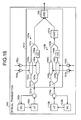
FIG. 18 is a block diagram of a tenth example of another configuration of the optical transmitter depicted in FIG. 1.
FIG. 19 is a block diagram of an eleventh example of another configuration of the optical transmitter depicted in FIG. 1.
FIG. 20 is a block diagram of a twelfth example of another configuration of the optical transmitter depicted in FIG. 1.
DESCRIPTION OF EMBODIMENTS
Preferred embodiments of the present invention will be explained with reference to the accompanying drawings. An optical transmission system according an embodiment improves SNR of polarized optical signals by a disposal of plural LDs on the transmission side, and compensates phase shifting occurring among the LDs by executing digital coherent detection that includes phase estimation for each polarization on the receiving side.
FIG. 1 is a diagram depicting a configuration an optical transmission system according to the embodiment. As depicted in FIG. 1, an optical transmission system 10 includes an optical transmitter 100 and an optical receiver 200. The optical transmitter 100 transmits optical signals through an optical transmission path 11 to the optical receiver 200. With reference to FIG. 1, configuration of the optical transmitter 100 will be described, while configuration of the optical receiver 200 will be described hereinafter (for example, with reference to FIGS. 2, and 9 to 20).
The optical transmitter 100 includes an LD 110 a (first light source), an optical branching unit 121 a, a wavelength locker 122 a, a polarization adjusting unit 130 a, a phase modulator 140 a (first phase modulator), a driving unit 151 a, a driving unit 152 a, an LD 110 b (second light source), an optical branching unit 121 b, a wavelength locker 122 b, a polarization adjusting unit 130 b, a phase modulator 140 b (second phase modulator), a driving unit 151 b, a driving unit 152 b, and a polarized beam combiner (PBC) 160.
The LD 110 a, the optical branching unit 121 a, the wavelength locker 122 a, the polarization adjusting unit 130 a, the phase modulator 140 a, the driving unit 151 a, and the driving unit 152 a generate light of a polarization X. LD 110 b, the optical branching unit 121 b, the wavelength locker 122 b, the polarization adjusting unit 130 b, the phase modulator 140 b, the driving unit 151 b, and the driving unit 152 b generate light of a polarization Y. Here, the polarization X and the polarization Y are orthogonal to one another.
The LD 110 a generates and outputs light to the optical branching unit 121 a. The LD 110 a also changes the wavelength of the light generated, under the control of the wavelength locker 122 a. The optical branching unit 121 a branches the light output from the LD 110 a and outputs the branched light to the wavelength locker 122 a and the polarization adjusting unit 130 a. The wavelength locker 122 a (WL) monitors the wavelength of the light output from the optical branching unit 121 a and controls the LD 110 a to keep the monitored wavelength constant.
The polarization adjusting unit 130 a (polarization controller (PC)) adjusts the polarization of the light output from the optical branching unit 121 a to the polarization X and outputs the adjusted light to the phase modulator 140 a. The phase modulator 140 a phase modulates the light output from the polarization adjusting unit 130 a, based on modulation data output by the driving unit 151 a and the driving unit 152 a.
For example, the phase modulator 140 a is implemented by a branching unit 141 a, an I arm 142 a, a Q arm 143 a, an interferometer 144 a, an interferometer 145 a, a phase shifter 146 a, and a combining unit 147 a disposed on a lithium niobate (LN) substrate. The branching unit 141 a branches the light output from the polarization adjusting unit 130 a and outputs the branched light to the I arm 142 a and the Q arm 143 a.
The I arm 142 a transmits the light output from the branching unit 141 a. The interferometer 144 a is disposed in the I arm 142 a. The interferometer 144 a branches and couples the light transmitted through the I arm 142 a. The interferometer 144 a also phase modulates one of the branches of light, based on the modulation data output by the driving unit 151 a. The interferometer 144 a outputs the coupled light to combining unit 147 a.
The Q arm 143 a transmits light output from the branching unit 141 a. The interferometer 145 a and the phase shifter 146 a are disposed in the Q arm 143 a. The interferometer 145 a branches and couples the light transmitted through the Q arm 143 a. The interferometer 145 a also phase modulates one of the branches of light, based on the modulation data output by the driving unit 152 a. The interferometer 145 a outputs the coupled light to the phase shifter 146 a.
The phase shifter 146 a delays the light output from the interferometer 145 a by π/2 and outputs the delayed light to the combining unit 147 a. The combining unit 147 a combines the light output from the I arm 142 a and the light output from the Q arm 143 a and outputs the combined light to the polarized beam combiner 160. The light output from the phase modulator 140 a to the polarized beam combiner 160 is an optical signal of the polarization X (QPSK modulation).
The driving unit 151 a outputs to the interferometer 144 a, modulation data for an I channel of the polarization X. The driving unit 152 a outputs to the interferometer 144 a, modulation data for a Q channel of the polarization X. Here, modulation data is single-ended input to the driving unit 151 a and the driving unit 152 a, respectively. The driving unit 151 a outputs the single-ended modulation data to the interferometer 144 a. The driving unit 152 a outputs the single-ended modulation data to the interferometer 145 a.
As configurations of the LD 110 b, the optical branching unit 121 b, the wavelength locker 122 b, the polarization adjusting unit 130 b, the phase modulator 140 b, the driving unit 151 b, and the driving unit 152 b correspond respectively to the LD 110 a, the optical branching unit 121 a, the wavelength locker 122 a, the polarization adjusting unit 130 a, the phase modulator 140 a, the driving unit 151 a, and the driving unit 152 a, description therefor is herein omitted, noting that the polarization adjusting unit 130 b adjusts the light from the optical branching unit 121 b to the polarization Y, and the light output from the phase modulator 140 b is an optical signal of the polarization Y (QPSK modulation).
The polarized beam combiner 160 combines the optical signal (polarization X) output from the phase modulator 140 a and the optical signal (polarization Y) output from the phase modulator 140 b and outputs the combined optical signals (DP-QPSK). The optical signal output from the polarized beam combiner 160 is transmitted through the optical transmission path 11 to the optical receiver 200.
Here, configuration has been described such that forward propagated light of the LD 110 a is branched by the optical branching unit 121 a, where one of the branches is monitored by the wavelength locker 122 a, however, backward propagated light of the LD 110 a may be monitored by the wavelength locker 122 a. Similarly, the backward propagated light of the LD 110 b may be monitored by the wavelength locker 122 b. In such cases, the optical branching unit 121 a and the optical branching unit 121 b may be omitted.
FIG. 2 is a block diagram of a first example of the optical receiver depicted in FIG. 1. As depicted in FIG. 2, the optical receiver 200 includes a first polarization beam splitter (PBS) 211, a local oscillator 212, a second PBS 213, optical hybrid circuits 220 a and 220 b, differential optical detectors 231 a, 232 a, 231 b, and 232 b, transimpedance amplifiers (TIAs) 241 a, 242 a, 241 b and 242 b, gain control amplifiers (GCAs) 251 a, 252 a, 251 b and 252 b, analog-digital converting units 261 a, 262 a, 261 b and 262 b, a digital signal processing unit 270, and an identifying unit 280.
The first PBS 211 receives the optical signal transmitted from the optical transmitter 100 (refer to FIG. 1) and splits the optical signal according to the polarization X and the polarization Y. The first PBS 211 outputs the optical signal of the polarization X to the optical hybrid circuit 220 a and outputs the optical signal of the polarization Y to the optical hybrid circuit 220 b.
The local oscillator 212 (LO_LD) generates light of a fixed frequency and outputs the generated light to the second PBS 213. The light output by the local oscillator 212 includes a component of the polarization X and a component of the polarization Y. The second PBS 213 splits the light output from the local oscillator 212, according to the polarization X and the polarization Y. The second PBS 213 outputs the optical signal of the polarization X to the optical hybrid circuit 220 a and outputs the optical signal of the polarization Y to the optical hybrid circuit 220 b.
The optical hybrid circuit 220 a, the differential optical detectors 231 a and 232 a, the TIAs 241 a and 242 a, the GCAs 251 a and 252 a, the analog-digital converting units 261 a and 262 a, the digital signal processing unit 270 and the identifying unit 280 configure a first digital coherent receiver that is of an intradyne configuration and corresponds to the phase modulator 140 a.
Further, the optical hybrid circuit 220 a, the differential optical detectors 231 a and 232 a, the TIAs 241 a and 242 a, and the GCAs 251 a and 252 a configure a frontend of the polarization X, outputting an electrical signal of a real part and an imaginary part of the optical signal of the polarization X. For example, the frontend of the polarization X, by a mixing of the light of the polarization X from the local oscillator 212 and the optical signal of the polarization X from the first PBS 211, outputs an electrical signal of a real part and an imaginary part.
The optical hybrid circuit 220 a (90° HYBRID) combines the optical signal from the first PBS 211 and the light from the second PBS 213 to generate 2 pairs of light differing in phase by 90°. For example, the optical hybrid circuit 220 a outputs 0°-phase light (S+R) and 180°-phase light (S−R) to the differential optical detector 231 a. Further, the optical hybrid circuit 220 a outputs 90°-phase light (S+jR) and 270°-phase light (S−jR) to the differential optical detector 232 a.
The differential optical detector 231 a receives the light (S+R) and the light (S−R) output from the optical hybrid circuit 220 a, detects the difference in power between the lights (S+R) and (S−R) for opto-electro conversion, and outputs the electrical signal obtained thereby to the TIA 241 a. The differential optical detector 232 a receives the light (S+jR) and the light (S−jR) output from the optical hybrid circuit 220 a, detects the difference in power between the lights (S+jR) and (S−jR) for opto-electro conversion, and outputs the electrical signal obtained hereby to the TIA 242 a.
The TIA 241 a amplifies the electrical signal output from the differential optical detector 231 a and outputs the amplified electrical signal to the GCA 251 a. The TIA 242 a amplifies the electrical signal output from the differential optical detector 232 a and outputs the amplified electrical signal to the GCA 252 a.
The GCA 251 a stabilizes the amplitude of the electrical signal output from the TIA 241 a and outputs the amplitude-controlled electrical signal to the analog-digital converting unit 261 a. The GCA 252 a stabilizes the amplitude of the electrical signal output from the TIA 242 a and outputs the amplitude-controlled electrical signal to the analog-digital converting unit 262 a.
The analog-digital converting unit 261 a (analog/digital converter (ADC)) converts the analog electrical signal output from the GCA 251 a into a digital signal and outputs the digital signal to the digital signal processing unit 270. The analog-digital converting unit 262 a converts the analog electrical signal output from the GCA 252 a and outputs the digital signal to the digital signal processing unit 270.
The digital signal processing unit 270 (digital signal processor (DSP)) performs phase estimation with respect to the digital signals (signal of the polarization X) output from the analog-digital converting units 261 a and 262 a, and extracts a signal. The digital signal processing unit 270 outputs the extracted signal to the identifying unit 280.
The optical hybrid circuit 220 b, the differential optical detector 231 b and 232 b, the TIAs 241 b and 242 b, the GCAs 251 b and 252 b, the analog-digital converting units 261 b and 262 b, the digital signal processing unit 270 and the identifying unit 280 configure a second coherent receiver that corresponds to the phase modulator 140 b.
Further, the optical hybrid circuit 220 b, the differential optical detector 231 b and 232 b, the TIAs 241 b and 242 b, the GCAs 251 b and 252 b configure a frontend of the polarization Y, outputting an electrical signal of a real part and an imaginary part of the optical signal of the polarization Y. For example, the frontend of the polarization Y, by a mixing of the light of the polarization Y from the local oscillator 212 and the optical signal of the polarization X from the first PBS 211, outputs an electrical signal of a real part and an imaginary part.
Configurations of the optical hybrid circuit 220 b, the differential optical detectors 231 b and 232 b, the TIAs 241 b and 242 b, the GCAs 251 b and 252 b, and the analog-digital converting units 261 b and 262 b respectively correspond to the configurations of the optical hybrid circuit 220 a and 220 b, the differential optical detectors 231 a and 232 a, the TIAs 241 a and 242 a, the GCAs 251 a and 252 a, and the analog-digital converting units 261 a and 262 a and thus, description therefor is omitted herein.
The digital signal processing unit 270 performs phase estimation with respect to the digital signals (signal of the polarization Y) output from the analog-digital converting units 261 b and 262 b, extracts a signal and outputs the extracted signal to the identifying unit 280. Further, the digital signal processing unit 270 may perform, in addition to phase estimation, other various types of digital processing such as dispersion compensation. The identifying unit 280 (DEC) identifies the signal output from the digital signal processing unit 270 and outputs an identification result.
FIG. 3 is a block diagram of a second example of the optical receiver. In FIG. 3, components identical to those depicted in FIG. 2 are given the same reference characters used in FIG. 2 and description therefor is omitted herein. As depicted in FIG. 3, the optical receiver 200 may have in addition to the configuration depicted in FIG. 2, low pass filters (LPFs) 311 a, 312 a, 311 b, and 312 b.
The LPF 311 a removes a high frequency component from the electrical signal output from the TIA 241 a to the LPF 311 a. Similarly, the LPFs 312 a, 311 b, and 312 b respectively extract high frequency components from the electrical signals respectively output from the TIAs 242 a, 241 b, and 242 b to the LPFs 312 a, 311 b, and 312 b. Thus, precision of the digital conversion at the analog-digital converting units 261 a, 262 a, 261 b, and 262 b can be improved.
FIG. 4 is a block diagram of a third example of the optical receiver. In FIG. 4, components identical to those depicted in FIG. 2 are given the same reference characters used in FIG. 2 and description therefor is omitted herein. As depicted in FIG. 4, the configuration depicted in FIG. 2 may be adapted such that the local oscillator 212, under the control of the digital signal processing unit 270, varies the frequency of the light output.
The digital signal processing unit 270, based on the result of digital processing with respect to the digital signals output from the analog-digital converting units 261 a, 262 a, 261 b, and 262 b, controls the frequency of the light output by the local oscillator 212. Thus, the frequency of the light output by the local oscillator 212 and the frequency of the optical signal can be made equivalent with high precision to enhance sensitivity in receiving the optical signal.
FIG. 5 is a flowchart of one example of frequency control at the digital signal processing unit depicted in FIG. 4. The digital signal processing unit 270, according to, for example, the following operations, controls the frequency of the light output by the local oscillator 212. Based on the digital signals output from the analog-digital converting units 261 a and 262 a, the digital signal processing unit 270 calculates the frequency difference Dx (frequency difference for the polarization X) between the frequency of the optical signal of the polarization X and the frequency of the light output by the local oscillator 212 (step S501).
Next, based on the digital signals output from the analog-digital converting units 261 b and 262 b, the digital signal processing unit 270 calculates the frequency difference Dy (difference for the polarization Y) between the frequency of the optical signal of the polarization Y and the frequency of the light output by the local oscillator 212 (step S502). The digital signal processing unit 270 further calculates a frequency adjustment value based on the frequency difference Dx calculated at step S501 and the frequency difference Dy calculated at step S502 (step S503).
According to the frequency adjustment value calculated at step S503, the digital signal processing unit 270 adjusts the frequency of the light output by the local oscillator 212 (step S504), ending series of operations. By repeating these operations, the digital signal processing unit 270 is able to control the frequency of the light output by the local oscillator 212. At step S503, for example, the average of the frequency difference Dx and the frequency difference Dy (Dx+Dy)/2 may be calculated as the frequency adjustment value.
In this example, although the digital signal processing unit 270 is described to calculate the frequency difference Dx and the frequency difference Dy, the frequency control performed at the digital signal processing unit 270 is not limited hereto and may be by another method. For example, the digital signal processing unit 270 may measure the quality Qx of the digital signals output from the analog-digital converting units 2Gla and 262 a and the quality Qy of the digital signal output from the analog-digital converting unit 261 b and 2G2 b, where the quality Qx and the quality Qy are, for example, bit error rate (BER).
The digital signal processing unit 270 calculates the frequency adjustment value such that the sum of the quality Qx and the quality Qy becomes large. Thus, the optical signal of the polarization X and the optical signal of the polarization Y can be received at maximum quality. Alternatively, the digital signal processing unit 270 may calculate the frequency adjustment value such that the difference between the quality Qx and the quality Qy becomes small. Thus, the optical signal of the polarization X and the optical signal of the polarization Y can be received at equivalent qualities.
FIG. 6 is a block diagram of a fourth example of the optical receiver. In FIG. 6, components identical to those depicted in FIG. 2 are given the same reference characters used in FIG. 2 and description therefor is omitted herein. As depicted in FIG. 6, the local oscillator 212 and the second PBS 213 in the configuration depicted in FIG. 2 may be replaced with a local oscillator 610 a and a local oscillator 610 b.
The local oscillator 610 a generates light of the polarization X and outputs the generated light to the optical hybrid circuit 220 a. The local oscillator 610 b generates light of the polarization Y and outputs the generated light to the optical hybrid circuit 220 b. Thus, light of sufficient power can be supplied to the optical hybrid circuit 220 a and the optical hybrid circuit 220 b, respectively.
FIG. 7 is a block diagram of a fifth example of the optical receiver. In FIG. 7, components identical to those depicted in FIG. 6 are given the same reference characters used in FIG. 6 and description therefor is omitted herein. As depicted in FIG. 7, the configuration depicted in FIG. 6 may be adapted such that the local oscillator 610 a and the local oscillator 610 b, under the control of the digital signal processing unit 270, vary the frequency of the light output.
The digital signal processing unit 270, based on the result of digital processing with respect to the digital signals output from the analog-digital converting units 261 a and 262 a, controls the frequency of the light output by the local oscillator 610 a. For example, the digital signal processing unit 270, based on the digital signal output from the analog-digital converting units 261 a and 262 a, calculates the frequency difference Dx between the frequency of the optical signal of the polarization X and the frequency of the light output from the local oscillator 610 a. The digital signal processing unit 270 further controls the local oscillator 610 a such that the frequency difference Dx becomes small.
Additionally, the digital signal processing unit 270, based on the digital signals output from the analog-digital converting units 261 b and 262 b, calculates the frequency difference Dy between the frequency of the optical signal of the polarization Y and the frequency of the light output from the local oscillator 610 b. The digital signal processing unit 270 further controls the local oscillator 610 b such that the frequency difference Dy become small. Thus, light of an optimal wavelength can be supplied to the local oscillator 610 a and the local oscillator 610 b, respectively. Consequently, the frequencies of the light output by the local oscillator 610 a and the local oscillator 610 b can be made identical to the frequencies of the polarizations of the optical signal with high precision to enhance sensitivity in receiving the optical signal.
FIG. 8 is a functional diagram of phase difference estimation at the digital signal processing unit. The digital signal processing unit 270 depicted in FIGS. 2 to 7 includes an argument calculating unit 810, a multiplying unit 820, a phase difference estimating unit 830, an averaging unit 840, and a demodulating unit 850.
Herein, description is given for phase difference estimation with respect to an optical signal of the polarization X in an optical signal received by the optical receiver 200, noting that phase difference estimation for an optical signal of the polarization Y is the same.
The digital signals output from the analog-digital converting unit 261 a and the analog-digital converting unit 262 a are input to the argument calculating unit 810 and the multiplying unit 820, respectively. The argument calculating unit 810 calculates an argument component of the input digital signal and outputs the argument component to the demodulating unit 850. The multiplying unit 820 multiples by 4, the electric field represented by the input digital signal and outputs the product to the phase difference estimating unit 830.
The phase difference estimating unit 830, based on the product output from the multiplying unit 820, estimates the phase difference between the optical signal output from the first PBS 211 and the light output from the second PBS 213. The phase difference estimating unit 830 outputs the estimated phase difference to the averaging unit 840. The averaging unit 840 averages the phase difference output from the phase difference estimating unit 830 by dividing the phase difference by 4 and outputs the averaged phase difference to the demodulating unit 850.
The demodulating unit 850, based on the argument component output from the argument calculating unit 810 and the phase difference output from the averaging unit 840, performs digital signal demodulation. The values for the multiplication at the multiplying unit 820 and for the division at the averaging unit 840 are determined by the modulation scheme of the optical light received by the optical receiver 200. Here, since the modulation scheme of the optical signal received by the optical receiver 200 is QPSK, the electric field is multiplied by 4 at the multiplying unit 820 and the phase difference is divided by 4 at the averaging unit 840.
FIG. 9 is a block diagram of a first example of another configuration of the optical transmitter depicted in FIG. 1. In FIG. 9 components identical to those depicted in FIG. 1 are given the same reference characters used in FIG. 1 and description therefor is omitted herein. As depicted in FIG. 9, the optical transmitter 100 may include in addition to the configuration depicted in FIG. 1, power monitors 921 a and 921 b, and power control units (power controllers) 922 a and 922 b.
The LD 110 a, under the control of the power control unit 922 a, varies the power of the light output. The power monitor 921 a monitors the power of the optical signal output from the combining unit 147 a and outputs the monitored power to the power control unit 922 a. The power control unit 922 a controls the LD 110 a such that the power indicated by the power monitor 921 a becomes stable.
The LD 110 b, under the control of the power control unit 922 b, varies the power of the light output. The power monitor 921 b monitors the power of the optical signal output from the combining unit 147 b and outputs the monitored power to the power control unit 922 b. The power control unit 922 b controls LD 110 b such that power indicated by the power monitor 921 b becomes constant.
Thus, the power of the optical signal of the polarization X generated by the phase modulator 140 a and the power of the optical signal of the polarization Y generated by the phase modulator 140 b are monitored, and the LD 110 a and the LD 110 b are controlled respectively such that the respectively monitored powers becomes constant. Thus, the power of the optical signal (DP-QPSK) transmitted from the optical transmitter 100 can be stabilized. Further, the power of each polarization included in the optical signal output from the optical transmitter 100 can be made equivalent.
FIG. 10 is a block diagram of a second example of another configuration of the optical transmitter depicted in FIG. 1. In FIG. 10 components identical to those depicted in FIG. 1 are given the same reference characters used in FIG. 1 and description therefor is omitted herein. As depicted in FIG. 10, the polarization adjusting unit 130 a may be omitted from the configuration depicted in FIG. 1. In this case, the LD 110 a outputs the light of polarization X.
Similarly, although not depicted, the polarization adjusting unit 130 b may be omitted from the configuration depicted in FIG. 1. In this case, the LD 110 b outputs the light of the polarization Y. Thus, a configuration to combine the polarized optical signals respectively generated by the phase modulator 140 a and the phase modulator 140 b is not limited to the configuration depicted in FIG. 1.
FIG. 11 is a block diagram of a third example of another configuration of the optical transmitter depicted in FIG. 1. In FIG. 11 components identical to those depicted in FIG. 1 are given the same reference characters used in FIG. 1 and description therefor is omitted herein. As depicted in FIG. 11, the polarization adjusting unit 130 a and the polarization adjusting unit 130 a may be disposed downstream from the phase modulator 140 a and the phase modulator 140 b, respectively. Thus, a configuration to combine the polarized optical signals respectively generated by the phase modulator 140 a and the phase modulator 140 b is not limited to the configuration depicted in FIG. 1.
FIG. 12 is a block diagram of a fourth example of another configuration of the optical transmitter depicted in FIG. 1. In FIG. 12 components identical to those depicted in FIG. 11 are given the same reference characters used in FIG. 11 and description therefor is omitted herein. As depicted in FIG. 12, the polarization adjusting unit 130 a may be omitted from the configuration depicted in FIG. 11. In this case, the LD 110 a outputs the light of polarization X.
Similarly, although not depicted, the polarization adjusting unit 130 b may be omitted from the configuration depicted in FIG. 11. In this case, the LD 110 b outputs the light of the polarization Y. Thus, a configuration to combine the polarized optical signals respectively generated by the phase modulator 140 a and the phase modulator 140 b is not limited to the configuration depicted in FIG. 1.
FIG. 13 is a block diagram of a fifth example of another configuration of the optical transmitter depicted in FIG. 1. In FIG. 13 components identical to those depicted in FIG. 12 are given the same reference characters used in FIG. 12 and description therefor is omitted herein. As depicted in FIG. 13, the polarization adjusting unit 130 a in the configuration depicted in FIG. 12 may be replaced with a half wave plate (HWP) 1310. The HWP 1310 shifts the optical signal output from the phase modulator 140 b to the polarized beam combiner 160, to the polarization Y.
Although not depicted, an HWP that shifts the optical signal to the polarization X may be disposed between the phase modulator 140 a and the polarized beam combiner 160. Further, the HWP 1310 may be disposed between the optical branching unit 121 b and the phase modulator 140 b. Furthermore, the configuration may be such that the HWP 1310 is disposed between the optical branching unit 121 b and the phase modulator 140 b, and an HWP that shifts light to the polarization X is disposed between the optical branching unit 121 a and the phase modulator 140 a.
FIG. 14 is a block diagram of a sixth example of another configuration of the optical transmitter depicted in FIG. 1. In FIG. 14 components identical to those depicted in FIG. 13 are given the same reference characters used in FIG. 13 and description therefor is omitted herein. As depicted in FIG. 14, in the configuration depicted in FIG. 13, the driving unit 151 a may output modulation data by a differential signal to the interferometer 144 a. For example, the driving unit 151 a may output the signals of a differential signal to each arm of the interferometer 144 a, respectively. Similarly, the driving units 152 a, 151 b, and 152 b may output modulation data by a differential signal to the interferometers 145 a, 144 b, and 145 b.
The interferometer 144 a, based on the differential signal output from the driving unit 151 a, modulates the light transmitted through the I arm 142 a. For example, the interferometer 144 a phase modulates one of the branches of light based on one of the differential signals output from the driving unit 151 a and phase modulates the other branch of light based on the other differential signal output from the driving unit 151 a. Similarly, the interferometers 145 a, 144 b, and 145 b modulate the light transmitted through the Q arm 143 a, the I arm 142 b, and the Q arm 143 b, based on the differential signals output from the driving units 152 a, 151 b, and 152 b. Thus, a configuration supplying modulation data is not limited to the configuration depicted in FIG. 1.
FIG. 15 is a block diagram of a seventh example of another configuration of the optical transmitter depicted in FIG. 1. In FIG. 15 components identical to those depicted in FIG. 14 are given the same reference characters used in FIG. 14 and description therefor is omitted herein. As depicted in FIG. 15, in the configuration depicted in FIG. 14, the driving units 151 a, 152 a, 151 b, and 152 b may receive modulation data by differential signals. Thus, a configuration supplying modulation data is not limited to the configuration depicted in FIG. 1.
FIG. 16 is a block diagram of an eighth example of another configuration of the optical transmitter depicted in FIG. 1. In FIG. 16 components identical to those depicted in FIG. 13 are given the same reference characters used in FIG. 13 and description therefor is omitted herein. As depicted in FIG. 16, in the configuration depicted in FIG. 13, the phase modulator 140 a, the phase modulator 140 b, the HWP 1310, and the polarized beam combiner 160 may be implemented disposed on an LN substrate 1610. Thus, a configuration integrating the components of the optical transmitter 100 is not limited to the configuration depicted in FIG. 1.
FIG. 17 is a block diagram of a ninth example of another configuration of the optical transmitter depicted in FIG. 1. In FIG. 17 components identical to those depicted in FIG. 13 are given the same reference characters used in FIG. 13 and description therefor is omitted herein. As depicted in FIG. 17, the optical transmitter 100 may include in addition to the configuration depicted in FIG. 13, an RZ (return to zero) modulator 1710 and a driving unit 1720, where the polarized beam combiner 160 outputs the combined optical signals to the RZ modulator 1710. The RZ modulator 1710 modulates the optical signal output from the polarized beam combiner 160 to a RZ pulse.
For example, an interferometer 1711 is disposed in the RZ modulator 1710, where the interferometer 1711 braches and combines light transmitted through the RZ modulator 1710. Further, the interferometer 1711 phase modulates one of the branches of light based on a clock signal output from a driving unit. The interferometer 1711 outputs combined light downstream. Thus, the optical signal output from the RZ modulator 1710 is modulated to an RZ pulse. The modulation of the optical signal to an RZ pulse enables sensitivity in receiving the optical signal at the optical receiver 200 to be enhanced. The driving unit 1720 outputs a clock signal to the RZ modulator 1710.
FIG. 18 is a block diagram of a tenth example of another configuration of the optical transmitter depicted in FIG. 1. In FIG. 18 components identical to those depicted in FIG. 13 are given the same reference characters used in FIG. 13 and description therefor is omitted herein. As depicted in FIG. 18, the optical transmitter 100 may include in addition to the configuration depicted in FIG. 13, RZ modulators 1810 a and 1810 b, and driving units 1820 a and 1820 b.
The RZ modulator 1810 a modulates the light output from the optical branching unit 121 a to a RZ pulse and outputs the RZ pulse to the phase modulator 140 a. The RZ modulator 1810 b modulates the light output from the optical branching unit 121 b to a RZ pulse and outputs the RZ pulse to the phase modulator 140 b. The driving unit 1820 a outputs a clock to the RZ modulator 1810 a and the driving unit 1820 b outputs a clock signal to the RZ modulator 1810 b.
The RZ pulse modulation of the light by the RZ modulator 1810 a and the RZ modulator 1810 b is identical to that of the RZ modulator 1710 depicted in FIG. 17 and description therefor is omitted herein. Through the configuration depicted in FIG. 18, the optical signals generated respectively by the phase modulator 140 a and the phase modulator 140 b are RZ pulse modulated, thereby enabling the optical signal (DP-QPSK) output from the polarized beam combiner 160 to be RZ pulse modulated.
FIG. 19 is a block diagram of an eleventh example of another configuration of the optical transmitter depicted in FIG. 1. In FIG. 19 components identical to those depicted in FIG. 18 are given the same reference characters used in FIG. 18 and description therefor is omitted herein. As depicted in FIG. 19, in the configuration depicted in FIG. 1, the RZ modulator 1810 a and the driving unit 1820 a may be disposed between the phase modulator 140 a and the polarized beam combiner 160. Further, the RZ modulator 1810 b and the driving unit 1820 b may be disposed between the phase modulator 140 b and the polarized beam combiner 160.
In this configuration as well, the optical signal (DP-QPSK) output from the polarized beam combiner 160 can be RZ pulse modulated. Further, in FIG. 19, the HWP 1310 is disposed between the optical branching unit 121 b and the phase modulator 140 b. Alternatively, the position of the HWP 1310 may be between the phase modulator 140 b and RZ modulator 1810 b or between the RZ modulator 1810 b and the polarized beam combiner 160.
FIG. 20 is a block diagram of a twelfth example of another configuration of the optical transmitter depicted in FIG. 1. In FIG. 20 components identical to those depicted in FIG. 18 are given the same reference characters used in FIG. 18 and description therefor is omitted herein. As depicted in FIG. 20, the optical transmitter 100 may include in place of the RZ modulator 1810 a and the driving unit 1820 a in the configuration depicted in FIG. 18, an electro absorption (EA) modulator 2010 a. Further, the optical transmitter 100 may include in place of the RZ modulator 1810 b and the driving unit 1820 b, an EA modulator 2010 b.
The EA modulator 2010 a receives the light output from the optical branching unit 121 a and a clock signal, and modulates the power of the light according to the clock signal; whereby the light is RZ pulse modulated. The EA modulator 2010 a outputs the RZ pulse to the phase modulator 140 a. Similarly, the EA modulator 2010 b RZ pulse modulates the light output from the optical branching unit 121 b and outputs the RZ pulse to the phase modulator 140 b.
Thus, by disposing the LD 110 a and the LD 110 b to generated light of the polarization X and light of the polarization Y, the respective powers thereof can be sufficiently secured. Consequently, even with application of an EA modulator as a modulator to RZ pulse modulate the light, RZ pulse modulation can be performed with good precision. By adopting an EA modulator, the size of the modulator for RZ pulse modulating the light can be reduced, facilitating a reduction in the size of the optical transmitter 100.
As described, according to the optical transmission system 10, the optical transmitter 100 is equipped with multiple LDs (the LD 110 a and 110 b) and from the light output by the LDs, optical signals of respective polarizations is generated. Thus, since optical signals of respective polarizations can be generated without branching the light from the LDs by a splitter, the power of each polarized optical signal can be sufficiently secured and the SNR thereof can be improved.
Further, by disposing the wavelength locker 122 a (first wavelength locker) controlling the wavelength of the LD 110 a and the wavelength locker 122 b (second wavelength locker) controlling the wavelength of the LD 110 b in the optical transmitter 100, differences in frequency between the LD 110 a and the LD 110 b can be reduced at optical transmitter 100. However, if the frequency of the LD 110 a and the LD 110 b is sufficiently stable, the wavelength lockers 122 a and 122 b may be omitted from the configuration of the optical transmitter 100.
By implementing an intradyne configuration of the optical receiver 200 to perform digital coherent detection that includes phase estimation for each polarized optical signal, phase shifting occurring between the LDs at the optical transmitter 100 can be compensated at the optical receiver 200. Thus, at the optical receiver 200, the optical signals can be received with good sensitivity without disposing OPLLs for each polarized optical signal. Consequently, the optical receiver 200, without having a large size, can improve the quality of optical transmissions from the optical transmitter 100 to the optical receiver 200.
For example, as depicted by the configurations in FIGS. 2 to 4, at the optical receiver 200, even if one local oscillator (the local oscillator 212) is disposed for the polarized optical signals, the optical signals can be received with good sensitivity. Further, in a configuration of the optical receiver 200 having one local oscillator 212, for example, as depicted in FIGS. 4 and 5, the frequency difference between the light from the local oscillator 212 and each optical signal separated by the first PBS 211 is calculated and based on the calculated frequency difference, the frequency of the light from the local oscillator 212 is controlled, thereby enabling the frequency difference between the polarized optical signals to be compensated to a certain extent.
In a configuration of the optical receiver 200 having one local oscillator 212, the quality of each optical signal, phase separated by the first PBS 211, is measured and the frequency of the light from the local oscillator 212 is controlled such that the sum of the measured qualities becomes large and thus, each polarization of light can be received at maximum quality. Alternatively, the frequency of the light from the local oscillator 212 can be controlled such that the difference between the measured qualities becomes small and thus, each polarized optical signal can be received at equivalent qualities.
Further, for example, as depicted in FIG. 9, the optical transmitter 100 may be configured to monitor the power of the light output by the phase modulators 140 a and 140 b, and based on the monitored power, control the power of the light output by the LD 110 a and the LD 110 b. Thus, differences in optical loss at components generating the polarized optical signals at the optical transmitter 100 can be reduced at the optical transmitter 100, thereby enabling the power of each polarized optical signal to be equivalent and consequently, the SNR thereof can be made equivalent.
In the embodiments, a configuration adopting a QPSK modulator (phase modulator 140 a and phase modulator 140 b) as the phase modulator of the optical transmitter 100 is described, however, the phase modulator is not limited a QPSK scheme. A differential QPSK (DQPSK) or binary PSK (BPSK) modulator may be adopted.
According to the configurations above, through a disposal of the first light source and the second light source in the optical transmitter, the power of each polarized optical signal is secured and phases differences between light sources at the optical transmitter can be compensated by phase estimation for each polarized optical signal in the digital coherent detection at the optical receiver.
All examples and conditional language recited herein are intended for pedagogical purposes to aid the reader in understanding the invention and the concepts contributed by the inventor to furthering the art, and are to be construed as being without limitation to such specifically recited examples and conditions, nor does the organization of such examples in the specification relate to a showing of the superiority and inferiority of the invention. Although the embodiments of the present invention have been described in detail, it should be understood that the various changes, substitutions, and alterations could be made hereto without departing from the spirit and scope of the invention.