US8299703B2 - Blue light emitting compound and organic light emitting diode device comprising the same - Google Patents
Blue light emitting compound and organic light emitting diode device comprising the same Download PDFInfo
- Publication number
- US8299703B2 US8299703B2 US12/630,589 US63058909A US8299703B2 US 8299703 B2 US8299703 B2 US 8299703B2 US 63058909 A US63058909 A US 63058909A US 8299703 B2 US8299703 B2 US 8299703B2
- Authority
- US
- United States
- Prior art keywords
- light emitting
- emitting diode
- organic light
- diode device
- following chemical
- Prior art date
- Legal status (The legal status is an assumption and is not a legal conclusion. Google has not performed a legal analysis and makes no representation as to the accuracy of the status listed.)
- Active, expires
Links
- 0 *C(c1ccc(C(Cc(cc2)cc3c2c(-c2ccccc2)c(cc(cc2)I4c(ccc(C(F)(F)I)c5)c5-c5c4ccc(C(F)(F)F)c5)c2c3-c2ccccc2)c2c-3cc(C(F)(I)[Tl])cc2)c-3c1)([Tl])[Fl] Chemical compound *C(c1ccc(C(Cc(cc2)cc3c2c(-c2ccccc2)c(cc(cc2)I4c(ccc(C(F)(F)I)c5)c5-c5c4ccc(C(F)(F)F)c5)c2c3-c2ccccc2)c2c-3cc(C(F)(I)[Tl])cc2)c-3c1)([Tl])[Fl] 0.000 description 25
- SQNUEBMTAGKTMB-UHFFFAOYSA-N CC1=CC2=C(C=C1C)N(C1=CC=C3C(=C1)C(C)=C1C=CC(N4C5=C(C=C(C)C(C)=C5)C5=C4C=C(C)C(C)=C5)=CC1=C3C)C1=C2C=C(C)C(C)=C1 Chemical compound CC1=CC2=C(C=C1C)N(C1=CC=C3C(=C1)C(C)=C1C=CC(N4C5=C(C=C(C)C(C)=C5)C5=C4C=C(C)C(C)=C5)=CC1=C3C)C1=C2C=C(C)C(C)=C1 SQNUEBMTAGKTMB-UHFFFAOYSA-N 0.000 description 6
- KWZVRQWLAFGPQP-UHFFFAOYSA-N C1=CC=C(C2=CC=CC(C3=CC=CC=C3)=C2)C=C1.C1=CC=C(C2=CC=CC=C2)C=C1.C1=CC=C2C(=C1)C=CC1=C2/C=C\C=C/1.C1=CC=C2C=CC=CC2=C1.C1=CC=C2C=CC=CC2=C1.C1=CC=CC=C1.C1=CC=NC=C1.CC.CC.CC.CC.CC.CC.CC.CC.CC.CC.CC.CC.CC.CC.CC.CC.CC.CC.CC.CC.CC.CC.CC.CC.CC.CC#N.CC(C)(C)C.CC(C)(C)C1=CC=C(C2=CC=CC=C2)C=C1.CC(C)(C)C1=CC=CC=C1.CC(C)C.CC(F)(F)F.CC1=CC=C(C)C=C1.CC1=CC=C(C2=CC=CC=C2)C=C1.CC1=CC=CC(C)=C1.CC1=CC=CC=C1.CC1=CC=CC=C1C.CC1=CC=CC=N1.CC1=CC=CN=C1.CCOC.CF.COC.C[Si](C)(C)C.C[Si](C)(C)C1=CC=C(C2=CC=CC=C2)C=C1.C[Si](C)(C)C1=CC=CC=C1.C[Si](C)(C)C1=CC=CC=N1.C[Si](C)(C)C1=CC=CN=C1.FC(F)(F)C1=CC=C(C2=CC=CC=C2)C=C1.FC(F)(F)C1=CC=CC=C1.FC1=CC=C(C2=CC=CC=C2)C=C1.FC1=CC=CC=C1.N#CC1=CC=C(C2=CC=CC=C2)C=C1.N#CC1=CC=CC=C1 Chemical compound C1=CC=C(C2=CC=CC(C3=CC=CC=C3)=C2)C=C1.C1=CC=C(C2=CC=CC=C2)C=C1.C1=CC=C2C(=C1)C=CC1=C2/C=C\C=C/1.C1=CC=C2C=CC=CC2=C1.C1=CC=C2C=CC=CC2=C1.C1=CC=CC=C1.C1=CC=NC=C1.CC.CC.CC.CC.CC.CC.CC.CC.CC.CC.CC.CC.CC.CC.CC.CC.CC.CC.CC.CC.CC.CC.CC.CC.CC.CC#N.CC(C)(C)C.CC(C)(C)C1=CC=C(C2=CC=CC=C2)C=C1.CC(C)(C)C1=CC=CC=C1.CC(C)C.CC(F)(F)F.CC1=CC=C(C)C=C1.CC1=CC=C(C2=CC=CC=C2)C=C1.CC1=CC=CC(C)=C1.CC1=CC=CC=C1.CC1=CC=CC=C1C.CC1=CC=CC=N1.CC1=CC=CN=C1.CCOC.CF.COC.C[Si](C)(C)C.C[Si](C)(C)C1=CC=C(C2=CC=CC=C2)C=C1.C[Si](C)(C)C1=CC=CC=C1.C[Si](C)(C)C1=CC=CC=N1.C[Si](C)(C)C1=CC=CN=C1.FC(F)(F)C1=CC=C(C2=CC=CC=C2)C=C1.FC(F)(F)C1=CC=CC=C1.FC1=CC=C(C2=CC=CC=C2)C=C1.FC1=CC=CC=C1.N#CC1=CC=C(C2=CC=CC=C2)C=C1.N#CC1=CC=CC=C1 KWZVRQWLAFGPQP-UHFFFAOYSA-N 0.000 description 4
- YPTCSNGPERYCMV-UHFFFAOYSA-N C1=CC2=CC=NC=C2C=C1.C1=CC=C(C2=CC=CC=N2)C=C1.C1=CC=C(C2=NC=CC=C2)C=C1.C1=CC=C(C2=NC=CC=C2)N=C1.C1=CN=C2C=CC=CC2=C1.CC.CC.CC.CC.CC.CC.CC.CC(C)(C)C1=CC=CC=N1.CC(C)(C)C1=CC=CN=C1.FC(F)(F)C1=CC=CC=N1.FC(F)(F)C1=CC=CN=C1 Chemical compound C1=CC2=CC=NC=C2C=C1.C1=CC=C(C2=CC=CC=N2)C=C1.C1=CC=C(C2=NC=CC=C2)C=C1.C1=CC=C(C2=NC=CC=C2)N=C1.C1=CN=C2C=CC=CC2=C1.CC.CC.CC.CC.CC.CC.CC.CC(C)(C)C1=CC=CC=N1.CC(C)(C)C1=CC=CN=C1.FC(F)(F)C1=CC=CC=N1.FC(F)(F)C1=CC=CN=C1 YPTCSNGPERYCMV-UHFFFAOYSA-N 0.000 description 2
- DQLLNGLPRIQKPD-UHFFFAOYSA-N C1=CC=C(C2=CC=CC(C3=CC=CC=C3)=C2)C=C1.C1=CC=C(C2=CC=CC=N2)C=C1.C1=CC=C(C2=NC=CC=C2)C=C1.C1=CC=C(C2=NC=CC=C2)N=C1.CC.CC.CC.CC.CC.CC.CC.CC.CC.CC.CC.CC.CC.CC.CC.CC.CC.CC.CC(C)(C)C1=CC=C(C2=CC=CC=C2)C=C1.CC(C)(C)C1=CC=CC=N1.CC(C)(C)C1=CC=CN=C1.CC(F)(F)C1=CC=CN=C1.C[Si](C)(C)C1=CC=C(C2=CC=CC=C2)C=C1.C[Si](C)(C)C1=CC=CC=C1.C[Si](C)(C)C1=CC=CC=N1.C[Si](C)(C)C1=CC=CN=C1.FC(F)(F)C1=CC=C(C2=CC=CC=C2)C=C1.FC(F)(F)C1=CC=CC=C1.FC(F)(F)C1=CC=CC=N1.FC1=CC=C(C2=CC=CC=C2)C=C1.FC1=CC=CC=C1.N#CC1=CC=C(C2=CC=CC=C2)C=C1.N#CC1=CC=CC=C1 Chemical compound C1=CC=C(C2=CC=CC(C3=CC=CC=C3)=C2)C=C1.C1=CC=C(C2=CC=CC=N2)C=C1.C1=CC=C(C2=NC=CC=C2)C=C1.C1=CC=C(C2=NC=CC=C2)N=C1.CC.CC.CC.CC.CC.CC.CC.CC.CC.CC.CC.CC.CC.CC.CC.CC.CC.CC.CC(C)(C)C1=CC=C(C2=CC=CC=C2)C=C1.CC(C)(C)C1=CC=CC=N1.CC(C)(C)C1=CC=CN=C1.CC(F)(F)C1=CC=CN=C1.C[Si](C)(C)C1=CC=C(C2=CC=CC=C2)C=C1.C[Si](C)(C)C1=CC=CC=C1.C[Si](C)(C)C1=CC=CC=N1.C[Si](C)(C)C1=CC=CN=C1.FC(F)(F)C1=CC=C(C2=CC=CC=C2)C=C1.FC(F)(F)C1=CC=CC=C1.FC(F)(F)C1=CC=CC=N1.FC1=CC=C(C2=CC=CC=C2)C=C1.FC1=CC=CC=C1.N#CC1=CC=C(C2=CC=CC=C2)C=C1.N#CC1=CC=CC=C1 DQLLNGLPRIQKPD-UHFFFAOYSA-N 0.000 description 2
- OPKAZNNAOKKMLB-UHFFFAOYSA-N C[Si](C)(C)C1=CC2=C(C=C1)N(C1=CC=C3C(=C1)C(C1=CC=C(C4=CC=C(C(F)(F)F)C=C4)C=C1)=C1C=CC(N4C5=C(C=C([Si](C)(C)C)C=C5)C5=C4C=CC([Si](C)(C)C)=C5)=CC1=C3C1=CC=C(C3=CC=C(C(F)(F)F)C=C3)C=C1)C1=C2C=C([Si](C)(C)C)C=C1.C[Si](C)(C)C1=CC=C(C2=CC=C(C3=C4C=CC(N5C6=C(C=C([Si](C)(C)C)C=C6)C6=C5C=CC([Si](C)(C)C)=C6)=CC4=C(C4=CC=C(C5=CC=C([Si](C)(C)C)C=C5)C=C4)C4=CC=C(N5C6=C(C=C([Si](C)(C)C)C=C6)C6=C5C=CC([Si](C)(C)C)=C6)C=C43)C=C2)C=C1 Chemical compound C[Si](C)(C)C1=CC2=C(C=C1)N(C1=CC=C3C(=C1)C(C1=CC=C(C4=CC=C(C(F)(F)F)C=C4)C=C1)=C1C=CC(N4C5=C(C=C([Si](C)(C)C)C=C5)C5=C4C=CC([Si](C)(C)C)=C5)=CC1=C3C1=CC=C(C3=CC=C(C(F)(F)F)C=C3)C=C1)C1=C2C=C([Si](C)(C)C)C=C1.C[Si](C)(C)C1=CC=C(C2=CC=C(C3=C4C=CC(N5C6=C(C=C([Si](C)(C)C)C=C6)C6=C5C=CC([Si](C)(C)C)=C6)=CC4=C(C4=CC=C(C5=CC=C([Si](C)(C)C)C=C5)C=C4)C4=CC=C(N5C6=C(C=C([Si](C)(C)C)C=C6)C6=C5C=CC([Si](C)(C)C)=C6)C=C43)C=C2)C=C1 OPKAZNNAOKKMLB-UHFFFAOYSA-N 0.000 description 2
- GRSSVTVNTRODCQ-UHFFFAOYSA-N [C-]#[N+]C1=CC2=C(C=C1)N(C1=CC=C3C(=C1)C(C1=C(C4=CC=CC=C4)C=CC=C1)=C1C=CC(N4C5=C(C=C(C#N)C=C5)C5=C4C=CC([N+]#[C-])=C5)=CC1=C3C1=C(C3=CC=CC=C3)C=CC=C1)C1=C2C=C(C#N)C=C1.[C-]#[N+]C1=CC2=C(C=C1)N(C1=CC=C3C(=C1)C(C1=CC=C(C4=CC=C(C(C)(C)C)C=C4)C=C1)=C1C=CC(N4C5=C(C=C(C#N)C=C5)C5=C4C=CC([N+]#[C-])=C5)=CC1=C3C1=CC=C(C3=CC=C(C(C)(C)C)C=C3)C=C1)C1=C2C=C(C#N)C=C1.[C-]#[N+]C1=CC2=C(C=C1)N(C1=CC=C3C(=C1)C(C1=CC=C(C4=CC=C([Si](C)(C)C)C=C4)C=C1)=C1C=CC(N4C5=C(C=C(C#N)C=C5)C5=C4C=CC([N+]#[C-])=C5)=CC1=C3C1=CC=C(C3=CC=C([Si](C)(C)C)C=C3)C=C1)C1=C2C=C(C#N)C=C1 Chemical compound [C-]#[N+]C1=CC2=C(C=C1)N(C1=CC=C3C(=C1)C(C1=C(C4=CC=CC=C4)C=CC=C1)=C1C=CC(N4C5=C(C=C(C#N)C=C5)C5=C4C=CC([N+]#[C-])=C5)=CC1=C3C1=C(C3=CC=CC=C3)C=CC=C1)C1=C2C=C(C#N)C=C1.[C-]#[N+]C1=CC2=C(C=C1)N(C1=CC=C3C(=C1)C(C1=CC=C(C4=CC=C(C(C)(C)C)C=C4)C=C1)=C1C=CC(N4C5=C(C=C(C#N)C=C5)C5=C4C=CC([N+]#[C-])=C5)=CC1=C3C1=CC=C(C3=CC=C(C(C)(C)C)C=C3)C=C1)C1=C2C=C(C#N)C=C1.[C-]#[N+]C1=CC2=C(C=C1)N(C1=CC=C3C(=C1)C(C1=CC=C(C4=CC=C([Si](C)(C)C)C=C4)C=C1)=C1C=CC(N4C5=C(C=C(C#N)C=C5)C5=C4C=CC([N+]#[C-])=C5)=CC1=C3C1=CC=C(C3=CC=C([Si](C)(C)C)C=C3)C=C1)C1=C2C=C(C#N)C=C1 GRSSVTVNTRODCQ-UHFFFAOYSA-N 0.000 description 2
- XYWIZAZLRFOOIU-UHFFFAOYSA-N C.CC1=C(/C2=C3\C=CC(Br)=C\C3=C(/C3=C(C)C=CC=C3)C3=CC=C(Br)C=C32)C=CC=C1.CC1=CC=CC=C1Br.O=C1C2=CC(Br)=CC=C2C(=O)C2=C1C=CC(Br)=C2 Chemical compound C.CC1=C(/C2=C3\C=CC(Br)=C\C3=C(/C3=C(C)C=CC=C3)C3=CC=C(Br)C=C32)C=CC=C1.CC1=CC=CC=C1Br.O=C1C2=CC(Br)=CC=C2C(=O)C2=C1C=CC(Br)=C2 XYWIZAZLRFOOIU-UHFFFAOYSA-N 0.000 description 1
- YJOMKWYIQXPHLK-UHFFFAOYSA-N C1=CC(C2=C3C=CC(N4C5=C(C=CC=C5)C5=C4C=CC=C5)=CC3=C(C3=CN=CC=C3)C3=CC=C(N4C5=C(C=CC=C5)C5=C4C=CC=C5)C=C32)=CN=C1.C1=CC2=C(C=C1)C=C(C1=C3C=CC(N4C5=C(C=CC=C5)C5=C4C=CC=C5)=CC3=C(C3=CC4=C(C=CC=C4)C=C3)C3=CC=C(N4C5=C(C=CC=C5)C5=C4C=CC=C5)C=C31)C=C2.C1=CC2=CC=CC(C3=C4C=CC(N5C6=C(C=CC=C6)C6=C5C=CC=C6)=CC4=C(C4=C5C=CC=CC5=CC=C4)C4=CC=C(N5C6=C(C=CC=C6)C6=C5C=CC=C6)C=C43)=C2C=C1.C1=CC=C(C2=CC(C3=CC=CC=C3)=CC(C3=C4C=CC(N5C6=C(C=CC=C6)C6=C5C=CC=C6)=CC4=C(C4=CC(C5=CC=CC=C5)=CC(C5=CC=CC=C5)=C4)C4=CC=C(N5C6=C(C=CC=C6)C6=C5C=CC=C6)C=C43)=C2)C=C1.C1=CN=C(C2=C3C=CC(N4C5=C(C=CC=C5)C5=C4C=CC=C5)=CC3=C(C3=NC=CC=C3)C3=CC=C(N4C5=C(C=CC=C5)C5=C4C=CC=C5)C=C32)C=C1.CC1=CC=C2C=CC=CC2=C1C1=C2C=CC(N3C4=C(C=CC=C4)C4=C3C=CC=C4)=CC2=C(C2=C3C=CC=CC3=CC=C2C)C2=CC=C(N3C4=C(C=CC=C4)C4=C3C=CC=C4)C=C21 Chemical compound C1=CC(C2=C3C=CC(N4C5=C(C=CC=C5)C5=C4C=CC=C5)=CC3=C(C3=CN=CC=C3)C3=CC=C(N4C5=C(C=CC=C5)C5=C4C=CC=C5)C=C32)=CN=C1.C1=CC2=C(C=C1)C=C(C1=C3C=CC(N4C5=C(C=CC=C5)C5=C4C=CC=C5)=CC3=C(C3=CC4=C(C=CC=C4)C=C3)C3=CC=C(N4C5=C(C=CC=C5)C5=C4C=CC=C5)C=C31)C=C2.C1=CC2=CC=CC(C3=C4C=CC(N5C6=C(C=CC=C6)C6=C5C=CC=C6)=CC4=C(C4=C5C=CC=CC5=CC=C4)C4=CC=C(N5C6=C(C=CC=C6)C6=C5C=CC=C6)C=C43)=C2C=C1.C1=CC=C(C2=CC(C3=CC=CC=C3)=CC(C3=C4C=CC(N5C6=C(C=CC=C6)C6=C5C=CC=C6)=CC4=C(C4=CC(C5=CC=CC=C5)=CC(C5=CC=CC=C5)=C4)C4=CC=C(N5C6=C(C=CC=C6)C6=C5C=CC=C6)C=C43)=C2)C=C1.C1=CN=C(C2=C3C=CC(N4C5=C(C=CC=C5)C5=C4C=CC=C5)=CC3=C(C3=NC=CC=C3)C3=CC=C(N4C5=C(C=CC=C5)C5=C4C=CC=C5)C=C32)C=C1.CC1=CC=C2C=CC=CC2=C1C1=C2C=CC(N3C4=C(C=CC=C4)C4=C3C=CC=C4)=CC2=C(C2=C3C=CC=CC3=CC=C2C)C2=CC=C(N3C4=C(C=CC=C4)C4=C3C=CC=C4)C=C21 YJOMKWYIQXPHLK-UHFFFAOYSA-N 0.000 description 1
- CTUPLFXZMBBVKW-UHFFFAOYSA-N C1=CC(C2=C3C=CC(N4C5=C(C=CC=C5)C5=C4C=CC=C5)=CC3=C(C3=CN=CC=C3)C3=CC=C(N4C5=C(C=CC=C5)C5=C4C=CC=C5)C=C32)=CN=C1.C1=CN=C(C2=C3C=CC(N4C5=C(C=CC=C5)C5=C4C=CC=C5)=CC3=C(C3=NC=CC=C3)C3=CC=C(N4C5=C(C=CC=C5)C5=C4C=CC=C5)C=C32)C=C1.CC1=CN=C(C2=C3C=CC(N4C5=C(C=CC=C5)C5=C4C=CC=C5)=CC3=C(C3=NC=C(C)C=C3)C3=CC=C(N4C5=C(C=CC=C5)C5=C4C=CC=C5)C=C32)C=C1 Chemical compound C1=CC(C2=C3C=CC(N4C5=C(C=CC=C5)C5=C4C=CC=C5)=CC3=C(C3=CN=CC=C3)C3=CC=C(N4C5=C(C=CC=C5)C5=C4C=CC=C5)C=C32)=CN=C1.C1=CN=C(C2=C3C=CC(N4C5=C(C=CC=C5)C5=C4C=CC=C5)=CC3=C(C3=NC=CC=C3)C3=CC=C(N4C5=C(C=CC=C5)C5=C4C=CC=C5)C=C32)C=C1.CC1=CN=C(C2=C3C=CC(N4C5=C(C=CC=C5)C5=C4C=CC=C5)=CC3=C(C3=NC=C(C)C=C3)C3=CC=C(N4C5=C(C=CC=C5)C5=C4C=CC=C5)C=C32)C=C1 CTUPLFXZMBBVKW-UHFFFAOYSA-N 0.000 description 1
- NNFSCBUIMNIDLI-UHFFFAOYSA-N C1=CC2=C(C=C1)C1=C(C=CC=C1)N2.CC1=C(C2=C3C=CC(Br)=CC3=C(C3=C(C)C=CC=C3)C3=CC=C(Br)C=C32)C=CC=C1.CC1=C(C2=C3C=CC(N4C5=C(C=CC=C5)C5=C4C=CC=C5)=CC3=C(C3=C(C)C=CC=C3)C3=CC=C(N4C5=C(C=CC=C5)C5=C4C=CC=C5)C=C32)C=CC=C1 Chemical compound C1=CC2=C(C=C1)C1=C(C=CC=C1)N2.CC1=C(C2=C3C=CC(Br)=CC3=C(C3=C(C)C=CC=C3)C3=CC=C(Br)C=C32)C=CC=C1.CC1=C(C2=C3C=CC(N4C5=C(C=CC=C5)C5=C4C=CC=C5)=CC3=C(C3=C(C)C=CC=C3)C3=CC=C(N4C5=C(C=CC=C5)C5=C4C=CC=C5)C=C32)C=CC=C1 NNFSCBUIMNIDLI-UHFFFAOYSA-N 0.000 description 1
- UBVKHFRLEVTCKY-UHFFFAOYSA-N C1=CC2=C(C=C1)C=C(C1=C3C=CC(N4C5=C(C=CC=C5)C5=C4C=CC=C5)=CC3=C(C3=CC4=C(C=CC=C4)C=C3)C3=CC=C(N4C5=C(C=CC=C5)C5=C4C=CC=C5)C=C31)C=C2.C1=CC=C(C2=CC(C3=CC=CC=C3)=CC(C3=C4C=CC(N5C6=C(C=CC=C6)C6=C5C=CC=C6)=CC4=C(C4=CC(C5=CC=CC=C5)=CC(C5=CC=CC=C5)=C4)C4=CC=C(N5C6=C(C=CC=C6)C6=C5C=CC=C6)C=C43)=C2)C=C1.CC1=CC=C2C=CC=CC2=C1C1=C2C=CC(N3C4=C(C=CC=C4)C4=C3C=CC=C4)=CC2=C(C2=C3C=CC=CC3=CC=C2C)C2=CC=C(N3C4=C(C=CC=C4)C4=C3C=CC=C4)C=C21 Chemical compound C1=CC2=C(C=C1)C=C(C1=C3C=CC(N4C5=C(C=CC=C5)C5=C4C=CC=C5)=CC3=C(C3=CC4=C(C=CC=C4)C=C3)C3=CC=C(N4C5=C(C=CC=C5)C5=C4C=CC=C5)C=C31)C=C2.C1=CC=C(C2=CC(C3=CC=CC=C3)=CC(C3=C4C=CC(N5C6=C(C=CC=C6)C6=C5C=CC=C6)=CC4=C(C4=CC(C5=CC=CC=C5)=CC(C5=CC=CC=C5)=C4)C4=CC=C(N5C6=C(C=CC=C6)C6=C5C=CC=C6)C=C43)=C2)C=C1.CC1=CC=C2C=CC=CC2=C1C1=C2C=CC(N3C4=C(C=CC=C4)C4=C3C=CC=C4)=CC2=C(C2=C3C=CC=CC3=CC=C2C)C2=CC=C(N3C4=C(C=CC=C4)C4=C3C=CC=C4)C=C21 UBVKHFRLEVTCKY-UHFFFAOYSA-N 0.000 description 1
- MVPQRHDYOOCFSB-UHFFFAOYSA-N C1=CC2=C(C=C1)N=C(C1=C3C=CC(N4C5=C(C=CC=C5)C5=C4C=CC=C5)=CC3=C(C3=NC4=C(C=CC=C4)C=C3)C3=CC=C(N4C5=C(C=CC=C5)C5=C4C=CC=C5)C=C31)C=C2.C1=CC2=CC=NC(C3=C4C=CC(N5C6=C(C=CC=C6)C6=C5C=CC=C6)=CC4=C(C4=C5C=CC=CC5=CC=N4)C4=CC=C(N5C6=C(C=CC=C6)C6=C5C=CC=C6)C=C43)=C2C=C1.C1=CC=C(C2=CN=C(C3=C4C=CC(N5C6=C(C=CC=C6)C6=C5C=CC=C6)=CC4=C(C4=NC=C(C5=CC=CC=C5)C=C4)C4=CC=C(N5C6=C(C=CC=C6)C6=C5C=CC=C6)C=C43)C=C2)C=C1.CC(C)(C)C1=CN=C(C2=C3C=CC(N4C5=C(C=CC=C5)C5=C4C=CC=C5)=CC3=C(C3=NC=C(C(C)(C)C)C=C3)C3=CC=C(N4C5=C(C=CC=C5)C5=C4C=CC=C5)C=C32)C=C1.CC1=CN=C(C2=C3C=CC(N4C5=C(C=CC=C5)C5=C4C=CC=C5)=CC3=C(C3=NC=C(C)C=C3)C3=CC=C(N4C5=C(C=CC=C5)C5=C4C=CC=C5)C=C32)C=C1.C[Si](C)(C)C1=CN=C(C2=C3C=CC(N4C5=C(C=CC=C5)C5=C4C=CC=C5)=CC3=C(C3=NC=C([Si](C)(C)C)C=C3)C3=CC=C(N4C5=C(C=CC=C5)C5=C4C=CC=C5)C=C32)C=C1 Chemical compound C1=CC2=C(C=C1)N=C(C1=C3C=CC(N4C5=C(C=CC=C5)C5=C4C=CC=C5)=CC3=C(C3=NC4=C(C=CC=C4)C=C3)C3=CC=C(N4C5=C(C=CC=C5)C5=C4C=CC=C5)C=C31)C=C2.C1=CC2=CC=NC(C3=C4C=CC(N5C6=C(C=CC=C6)C6=C5C=CC=C6)=CC4=C(C4=C5C=CC=CC5=CC=N4)C4=CC=C(N5C6=C(C=CC=C6)C6=C5C=CC=C6)C=C43)=C2C=C1.C1=CC=C(C2=CN=C(C3=C4C=CC(N5C6=C(C=CC=C6)C6=C5C=CC=C6)=CC4=C(C4=NC=C(C5=CC=CC=C5)C=C4)C4=CC=C(N5C6=C(C=CC=C6)C6=C5C=CC=C6)C=C43)C=C2)C=C1.CC(C)(C)C1=CN=C(C2=C3C=CC(N4C5=C(C=CC=C5)C5=C4C=CC=C5)=CC3=C(C3=NC=C(C(C)(C)C)C=C3)C3=CC=C(N4C5=C(C=CC=C5)C5=C4C=CC=C5)C=C32)C=C1.CC1=CN=C(C2=C3C=CC(N4C5=C(C=CC=C5)C5=C4C=CC=C5)=CC3=C(C3=NC=C(C)C=C3)C3=CC=C(N4C5=C(C=CC=C5)C5=C4C=CC=C5)C=C32)C=C1.C[Si](C)(C)C1=CN=C(C2=C3C=CC(N4C5=C(C=CC=C5)C5=C4C=CC=C5)=CC3=C(C3=NC=C([Si](C)(C)C)C=C3)C3=CC=C(N4C5=C(C=CC=C5)C5=C4C=CC=C5)C=C32)C=C1 MVPQRHDYOOCFSB-UHFFFAOYSA-N 0.000 description 1
- DNPRKHUPWISIRI-UHFFFAOYSA-N C1=CC2=C(C=C1)N=C(C1=C3C=CC(N4C5=C(C=CC=C5)C5=C4C=CC=C5)=CC3=C(C3=NC4=C(C=CC=C4)C=C3)C3=CC=C(N4C5=C(C=CC=C5)C5=C4C=CC=C5)C=C31)C=C2.C1=CC=C(C2=CN=C(C3=C4C=CC(N5C6=C(C=CC=C6)C6=C5C=CC=C6)=CC4=C(C4=NC=C(C5=CC=CC=C5)C=C4)C4=CC=C(N5C6=C(C=CC=C6)C6=C5C=CC=C6)C=C43)C=C2)C=C1.C1=CN=C(C2=CC=C(C3=C4C=CC(N5C6=C(C=CC=C6)C6=C5C=CC=C6)=CC4=C(C4=CC=C(C5=NC=CC=C5)C=C4)C4=CC=C(N5C6=C(C=CC=C6)C6=C5C=CC=C6)C=C43)C=C2)C=C1 Chemical compound C1=CC2=C(C=C1)N=C(C1=C3C=CC(N4C5=C(C=CC=C5)C5=C4C=CC=C5)=CC3=C(C3=NC4=C(C=CC=C4)C=C3)C3=CC=C(N4C5=C(C=CC=C5)C5=C4C=CC=C5)C=C31)C=C2.C1=CC=C(C2=CN=C(C3=C4C=CC(N5C6=C(C=CC=C6)C6=C5C=CC=C6)=CC4=C(C4=NC=C(C5=CC=CC=C5)C=C4)C4=CC=C(N5C6=C(C=CC=C6)C6=C5C=CC=C6)C=C43)C=C2)C=C1.C1=CN=C(C2=CC=C(C3=C4C=CC(N5C6=C(C=CC=C6)C6=C5C=CC=C6)=CC4=C(C4=CC=C(C5=NC=CC=C5)C=C4)C4=CC=C(N5C6=C(C=CC=C6)C6=C5C=CC=C6)C=C43)C=C2)C=C1 DNPRKHUPWISIRI-UHFFFAOYSA-N 0.000 description 1
- LLIOMJRRYPSFBN-UHFFFAOYSA-N C1=CC2=CC(C3=C4C=CC(N5C6=C(C=CC=C6)C6=C5C=CC=C6)=CC4=C(C4=C5C=CC=CC5=C5C=CC=CC5=C4)C4=CC=C(N5C6=C(C=CC=C6)C6=C5C=CC=C6)C=C43)=C3C=CC=CC3=C2C=C1.C1=CC2=CC=CC(C3=C4C=CC(N5C6=C(C=CC=C6)C6=C5C=CC=C6)=CC4=C(C4=C5C=CC=CC5=CC=C4)C4=CC=C(N5C6=C(C=CC=C6)C6=C5C=CC=C6)C=C43)=C2C=C1.FC1=CC=C(C2=CC=C(C3=C4C=CC(N5C6=C(C=CC=C6)C6=C5C=CC=C6)=CC4=C(C4=CC=C(C5=CC=C(F)C=C5)C=C4)C4=CC=C(N5C6=C(C=CC=C6)C6=C5C=CC=C6)C=C43)C=C2)C=C1 Chemical compound C1=CC2=CC(C3=C4C=CC(N5C6=C(C=CC=C6)C6=C5C=CC=C6)=CC4=C(C4=C5C=CC=CC5=C5C=CC=CC5=C4)C4=CC=C(N5C6=C(C=CC=C6)C6=C5C=CC=C6)C=C43)=C3C=CC=CC3=C2C=C1.C1=CC2=CC=CC(C3=C4C=CC(N5C6=C(C=CC=C6)C6=C5C=CC=C6)=CC4=C(C4=C5C=CC=CC5=CC=C4)C4=CC=C(N5C6=C(C=CC=C6)C6=C5C=CC=C6)C=C43)=C2C=C1.FC1=CC=C(C2=CC=C(C3=C4C=CC(N5C6=C(C=CC=C6)C6=C5C=CC=C6)=CC4=C(C4=CC=C(C5=CC=C(F)C=C5)C=C4)C4=CC=C(N5C6=C(C=CC=C6)C6=C5C=CC=C6)C=C43)C=C2)C=C1 LLIOMJRRYPSFBN-UHFFFAOYSA-N 0.000 description 1
- VMAINMFVSYAWJW-UHFFFAOYSA-N C1=CC2=CC(C3=C4C=CC(N5C6=C(C=CC=C6)C6=C5C=CC=C6)=CC4=C(C4=C5C=CC=CC5=C5C=CC=CC5=C4)C4=CC=C(N5C6=C(C=CC=C6)C6=C5C=CC=C6)C=C43)=C3C=CC=CC3=C2C=C1.FC1=CC=C(C2=CC=C(C3=C4C=CC(N5C6=C(C=CC=C6)C6=C5C=CC=C6)=CC4=C(C4=CC=C(C5=CC=C(F)C=C5)C=C4)C4=CC=C(N5C6=C(C=CC=C6)C6=C5C=CC=C6)C=C43)C=C2)C=C1.[C-]#[N+]C1=CC=C(C2=CC=C(C3=C4C=C(N5C6=C(C=CC=C6)C6=C5C=CC=C6)C=CC4=C(C4=CC=C(C5=CC=C(C#N)C=C5)C=C4)C4=CC(N5C6=C(C=CC=C6)C6=C5C=CC=C6)=CC=C43)C=C2)C=C1 Chemical compound C1=CC2=CC(C3=C4C=CC(N5C6=C(C=CC=C6)C6=C5C=CC=C6)=CC4=C(C4=C5C=CC=CC5=C5C=CC=CC5=C4)C4=CC=C(N5C6=C(C=CC=C6)C6=C5C=CC=C6)C=C43)=C3C=CC=CC3=C2C=C1.FC1=CC=C(C2=CC=C(C3=C4C=CC(N5C6=C(C=CC=C6)C6=C5C=CC=C6)=CC4=C(C4=CC=C(C5=CC=C(F)C=C5)C=C4)C4=CC=C(N5C6=C(C=CC=C6)C6=C5C=CC=C6)C=C43)C=C2)C=C1.[C-]#[N+]C1=CC=C(C2=CC=C(C3=C4C=C(N5C6=C(C=CC=C6)C6=C5C=CC=C6)C=CC4=C(C4=CC=C(C5=CC=C(C#N)C=C5)C=C4)C4=CC(N5C6=C(C=CC=C6)C6=C5C=CC=C6)=CC=C43)C=C2)C=C1 VMAINMFVSYAWJW-UHFFFAOYSA-N 0.000 description 1
- PPTUYYUCMLXAJE-UHFFFAOYSA-N C1=CC2=CC=NC(C3=C4C=CC(N5C6=C(C=CC=C6)C6=C5C=CC=C6)=CC4=C(C4=C5C=CC=CC5=CC=N4)C4=CC=C(N5C6=C(C=CC=C6)C6=C5C=CC=C6)C=C43)=C2C=C1.CC(C)(C)C1=CN=C(C2=C3C=CC(N4C5=C(C=CC=C5)C5=C4C=CC=C5)=CC3=C(C3=NC=C(C(C)(C)C)C=C3)C3=CC=C(N4C5=C(C=CC=C5)C5=C4C=CC=C5)C=C32)C=C1.C[Si](C)(C)C1=CN=C(C2=C3C=CC(N4C5=C(C=CC=C5)C5=C4C=CC=C5)=CC3=C(C3=NC=C([Si](C)(C)C)C=C3)C3=CC=C(N4C5=C(C=CC=C5)C5=C4C=CC=C5)C=C32)C=C1 Chemical compound C1=CC2=CC=NC(C3=C4C=CC(N5C6=C(C=CC=C6)C6=C5C=CC=C6)=CC4=C(C4=C5C=CC=CC5=CC=N4)C4=CC=C(N5C6=C(C=CC=C6)C6=C5C=CC=C6)C=C43)=C2C=C1.CC(C)(C)C1=CN=C(C2=C3C=CC(N4C5=C(C=CC=C5)C5=C4C=CC=C5)=CC3=C(C3=NC=C(C(C)(C)C)C=C3)C3=CC=C(N4C5=C(C=CC=C5)C5=C4C=CC=C5)C=C32)C=C1.C[Si](C)(C)C1=CN=C(C2=C3C=CC(N4C5=C(C=CC=C5)C5=C4C=CC=C5)=CC3=C(C3=NC=C([Si](C)(C)C)C=C3)C3=CC=C(N4C5=C(C=CC=C5)C5=C4C=CC=C5)C=C32)C=C1 PPTUYYUCMLXAJE-UHFFFAOYSA-N 0.000 description 1
- LEYVYFVFEWORRT-UHFFFAOYSA-N C1=CC=C(C2=C(C3=C4C=CC(N5C6=C(C=CC=C6)C6=C5C=CC=C6)=CC4=C(C4=C(C5=CC=CC=C5)C=CC=C4)C4=CC=C(N5C6=C(C=CC=C6)C6=C5C=CC=C6)C=C43)C=CC=C2)C=C1.C1=CC=C(C2=CC=C(C3=C4C=CC(N5C6=C(C=CC=C6)C6=C5C=CC=C6)=CC4=C(C4=CC=C(C5=CC=CC=C5)C=C4)C4=CC=C(N5C6=C(C=CC=C6)C6=C5C=CC=C6)C=C43)C=C2)C=C1.C1=CC=C(C2=CC=CC(C3=C4C=CC(N5C6=C(C=CC=C6)C6=C5C=CC=C6)=CC4=C(C4=CC(C5=CC=CC=C5)=CC=C4)C4=CC=C(N5C6=C(C=CC=C6)C6=C5C=CC=C6)C=C43)=C2)C=C1 Chemical compound C1=CC=C(C2=C(C3=C4C=CC(N5C6=C(C=CC=C6)C6=C5C=CC=C6)=CC4=C(C4=C(C5=CC=CC=C5)C=CC=C4)C4=CC=C(N5C6=C(C=CC=C6)C6=C5C=CC=C6)C=C43)C=CC=C2)C=C1.C1=CC=C(C2=CC=C(C3=C4C=CC(N5C6=C(C=CC=C6)C6=C5C=CC=C6)=CC4=C(C4=CC=C(C5=CC=CC=C5)C=C4)C4=CC=C(N5C6=C(C=CC=C6)C6=C5C=CC=C6)C=C43)C=C2)C=C1.C1=CC=C(C2=CC=CC(C3=C4C=CC(N5C6=C(C=CC=C6)C6=C5C=CC=C6)=CC4=C(C4=CC(C5=CC=CC=C5)=CC=C4)C4=CC=C(N5C6=C(C=CC=C6)C6=C5C=CC=C6)C=C43)=C2)C=C1 LEYVYFVFEWORRT-UHFFFAOYSA-N 0.000 description 1
- KKDMQRTUVOJMRV-UHFFFAOYSA-N C1=CC=C(C2=C(C3=C4C=CC(N5C6=C(C=CC=C6)C6=C5C=CC=C6)=CC4=C(C4=C(C5=CC=CC=C5)C=CC=C4)C4=CC=C(N5C6=C(C=CC=C6)C6=C5C=CC=C6)C=C43)C=CC=C2)C=C1.C1=CC=C(C2=CC=C(C3=C4C=CC(N5C6=C(C=CC=C6)C6=C5C=CC=C6)=CC4=C(C4=CC=C(C5=CC=CC=C5)C=C4)C4=CC=C(N5C6=C(C=CC=C6)C6=C5C=CC=C6)C=C43)C=C2)C=C1.C1=CC=C(C2=CC=CC(C3=C4C=CC(N5C6=C(C=CC=C6)C6=C5C=CC=C6)=CC4=C(C4=CC(C5=CC=CC=C5)=CC=C4)C4=CC=C(N5C6=C(C=CC=C6)C6=C5C=CC=C6)C=C43)=C2)C=C1.C[Si](C)(C)C1=CC=C(C2=C3C=CC(N4C5=C(C=CC=C5)C5=C4C=CC=C5)=CC3=C(C3=CC=C([Si](C)(C)C)C=C3)C3=CC=C(N4C5=C(C=CC=C5)C5=C4C=CC=C5)C=C32)C=C1.FC1=CC=C(C2=C3C=CC(N4C5=C(C=CC=C5)C5=C4C=CC=C5)=CC3=C(C3=CC=C(F)C=C3)C3=CC=C(N4C5=C(C=CC=C5)C5=C4C=CC=C5)C=C32)C=C1.[C-]#[N+]C1=CC=C(C2=C3C=C(N4C5=C(C=CC=C5)C5=C4C=CC=C5)C=CC3=C(C3=CC=C(C#N)C=C3)C3=CC(N4C5=C(C=CC=C5)C5=C4C=CC=C5)=CC=C32)C=C1 Chemical compound C1=CC=C(C2=C(C3=C4C=CC(N5C6=C(C=CC=C6)C6=C5C=CC=C6)=CC4=C(C4=C(C5=CC=CC=C5)C=CC=C4)C4=CC=C(N5C6=C(C=CC=C6)C6=C5C=CC=C6)C=C43)C=CC=C2)C=C1.C1=CC=C(C2=CC=C(C3=C4C=CC(N5C6=C(C=CC=C6)C6=C5C=CC=C6)=CC4=C(C4=CC=C(C5=CC=CC=C5)C=C4)C4=CC=C(N5C6=C(C=CC=C6)C6=C5C=CC=C6)C=C43)C=C2)C=C1.C1=CC=C(C2=CC=CC(C3=C4C=CC(N5C6=C(C=CC=C6)C6=C5C=CC=C6)=CC4=C(C4=CC(C5=CC=CC=C5)=CC=C4)C4=CC=C(N5C6=C(C=CC=C6)C6=C5C=CC=C6)C=C43)=C2)C=C1.C[Si](C)(C)C1=CC=C(C2=C3C=CC(N4C5=C(C=CC=C5)C5=C4C=CC=C5)=CC3=C(C3=CC=C([Si](C)(C)C)C=C3)C3=CC=C(N4C5=C(C=CC=C5)C5=C4C=CC=C5)C=C32)C=C1.FC1=CC=C(C2=C3C=CC(N4C5=C(C=CC=C5)C5=C4C=CC=C5)=CC3=C(C3=CC=C(F)C=C3)C3=CC=C(N4C5=C(C=CC=C5)C5=C4C=CC=C5)C=C32)C=C1.[C-]#[N+]C1=CC=C(C2=C3C=C(N4C5=C(C=CC=C5)C5=C4C=CC=C5)C=CC3=C(C3=CC=C(C#N)C=C3)C3=CC(N4C5=C(C=CC=C5)C5=C4C=CC=C5)=CC=C32)C=C1 KKDMQRTUVOJMRV-UHFFFAOYSA-N 0.000 description 1
- GOIJYHNIMSESQD-UHFFFAOYSA-N C1=CC=C(C2=C3C=CC(N4C5=C(C=CC=C5)C5=C4C=CC=C5)=CC3=C(C3=CC=CC=C3)C3=CC=C(N4C5=C(C=CC=C5)C5=C4C=CC=C5)C=C32)C=C1.CC(C)(C)C1=CC=C(C2=C3C=CC(N4C5=C(C=CC=C5)C5=C4C=CC=C5)=CC3=C(C3=CC=C(C(C)(C)C)C=C3)C3=CC=C(N4C5=C(C=CC=C5)C5=C4C=CC=C5)C=C32)C=C1.CC(F)(F)C1=CC=C(C2=C3C=CC(N4C5=C(C=CC=C5)C5=C4C=CC=C5)=CC3=C(C3=CC=C(C(F)(F)F)C=C3)C3=CC=C(N4C5=C(C=CC=C5)C5=C4C=CC=C5)C=C32)C=C1.CC1=C(C2=C3C=CC(N4C5=C(C=CC=C5)C5=C4C=CC=C5)=CC3=C(C3=C(C)C=CC=C3)C3=CC=C(N4C5=C(C=CC=C5)C5=C4C=CC=C5)C=C32)C=CC=C1.CC1=CC=C(C2=C3C=CC(N4C5=C(C=CC=C5)C5=C4C=CC=C5)=CC3=C(C3=CC=C(C)C=C3)C3=CC=C(N4C5=C(C=CC=C5)C5=C4C=CC=C5)C=C32)C=C1.CC1=CC=CC(C2=C3C=CC(N4C5=C(C=CC=C5)C5=C4C=CC=C5)=CC3=C(C3=CC(C)=CC=C3)C3=CC=C(N4C5=C(C=CC=C5)C5=C4C=CC=C5)C=C32)=C1 Chemical compound C1=CC=C(C2=C3C=CC(N4C5=C(C=CC=C5)C5=C4C=CC=C5)=CC3=C(C3=CC=CC=C3)C3=CC=C(N4C5=C(C=CC=C5)C5=C4C=CC=C5)C=C32)C=C1.CC(C)(C)C1=CC=C(C2=C3C=CC(N4C5=C(C=CC=C5)C5=C4C=CC=C5)=CC3=C(C3=CC=C(C(C)(C)C)C=C3)C3=CC=C(N4C5=C(C=CC=C5)C5=C4C=CC=C5)C=C32)C=C1.CC(F)(F)C1=CC=C(C2=C3C=CC(N4C5=C(C=CC=C5)C5=C4C=CC=C5)=CC3=C(C3=CC=C(C(F)(F)F)C=C3)C3=CC=C(N4C5=C(C=CC=C5)C5=C4C=CC=C5)C=C32)C=C1.CC1=C(C2=C3C=CC(N4C5=C(C=CC=C5)C5=C4C=CC=C5)=CC3=C(C3=C(C)C=CC=C3)C3=CC=C(N4C5=C(C=CC=C5)C5=C4C=CC=C5)C=C32)C=CC=C1.CC1=CC=C(C2=C3C=CC(N4C5=C(C=CC=C5)C5=C4C=CC=C5)=CC3=C(C3=CC=C(C)C=C3)C3=CC=C(N4C5=C(C=CC=C5)C5=C4C=CC=C5)C=C32)C=C1.CC1=CC=CC(C2=C3C=CC(N4C5=C(C=CC=C5)C5=C4C=CC=C5)=CC3=C(C3=CC(C)=CC=C3)C3=CC=C(N4C5=C(C=CC=C5)C5=C4C=CC=C5)C=C32)=C1 GOIJYHNIMSESQD-UHFFFAOYSA-N 0.000 description 1
- FGTJAIUINNLFNX-UHFFFAOYSA-N C1=CC=C(C2=C3C=CC(N4C5=C(C=CC=C5)C5=C4C=CC=C5)=CC3=C(C3=CC=CC=C3)C3=CC=C(N4C5=C(C=CC=C5)C5=C4C=CC=C5)C=C32)C=C1.CC1=C(C2=C3C=CC(N4C5=C(C=CC=C5)C5=C4C=CC=C5)=CC3=C(C3=C(C)C=CC=C3)C3=CC=C(N4C5=C(C=CC=C5)C5=C4C=CC=C5)C=C32)C=CC=C1.CC1=CC=CC(C2=C3C=CC(N4C5=C(C=CC=C5)C5=C4C=CC=C5)=CC3=C(C3=CC(C)=CC=C3)C3=CC=C(N4C5=C(C=CC=C5)C5=C4C=CC=C5)C=C32)=C1 Chemical compound C1=CC=C(C2=C3C=CC(N4C5=C(C=CC=C5)C5=C4C=CC=C5)=CC3=C(C3=CC=CC=C3)C3=CC=C(N4C5=C(C=CC=C5)C5=C4C=CC=C5)C=C32)C=C1.CC1=C(C2=C3C=CC(N4C5=C(C=CC=C5)C5=C4C=CC=C5)=CC3=C(C3=C(C)C=CC=C3)C3=CC=C(N4C5=C(C=CC=C5)C5=C4C=CC=C5)C=C32)C=CC=C1.CC1=CC=CC(C2=C3C=CC(N4C5=C(C=CC=C5)C5=C4C=CC=C5)=CC3=C(C3=CC(C)=CC=C3)C3=CC=C(N4C5=C(C=CC=C5)C5=C4C=CC=C5)C=C32)=C1 FGTJAIUINNLFNX-UHFFFAOYSA-N 0.000 description 1
- IMTPEKPKCUTOIH-UHFFFAOYSA-N C1=CC=C(C2=CC(C3=NC=CC=C3)=CC(C3=C4C=CC(N5C6=C(C=CC=C6)C6=C5C=CC=C6)=CC4=C(C4=CC(C5=CC=CC=N5)=CC(C5=NC=CC=C5)=C4)C4=CC=C(N5C6=C(C=CC=C6)C6=C5C=CC=C6)C=C43)=C2)N=C1.C1=CN=C(C2=CC=C(C3=C4C=CC(N5C6=C(C=CC=C6)C6=C5C=CC=C6)=CC4=C(C4=CC=C(C5=NC=CC=C5)C=C4)C4=CC=C(N5C6=C(C=CC=C6)C6=C5C=CC=C6)C=C43)C=C2)C=C1.CC1=C(C2=C3C=CC(N4C5=C(C=C([Si](C)(C)C)C=C5)C5=C4C=CC([Si](C)(C)C)=C5)=CC3=C(C3=C(C)C=CC=C3)C3=CC=C(N4C5=C(C=C([Si](C)(C)C)C=C5)C5=C4C=CC([Si](C)(C)C)=C5)C=C32)C=CC=C1.C[Si](C)(C)C1=CC2=C(C=C1)N(C1=CC=C3C(=C1)C(C1=CC=CC=C1)=C1C=CC(N4C5=C(C=C([Si](C)(C)C)C=C5)C5=C4C=CC([Si](C)(C)C)=C5)=CC1=C3C1=CC=CC=C1)C1=C2C=C([Si](C)(C)C)C=C1 Chemical compound C1=CC=C(C2=CC(C3=NC=CC=C3)=CC(C3=C4C=CC(N5C6=C(C=CC=C6)C6=C5C=CC=C6)=CC4=C(C4=CC(C5=CC=CC=N5)=CC(C5=NC=CC=C5)=C4)C4=CC=C(N5C6=C(C=CC=C6)C6=C5C=CC=C6)C=C43)=C2)N=C1.C1=CN=C(C2=CC=C(C3=C4C=CC(N5C6=C(C=CC=C6)C6=C5C=CC=C6)=CC4=C(C4=CC=C(C5=NC=CC=C5)C=C4)C4=CC=C(N5C6=C(C=CC=C6)C6=C5C=CC=C6)C=C43)C=C2)C=C1.CC1=C(C2=C3C=CC(N4C5=C(C=C([Si](C)(C)C)C=C5)C5=C4C=CC([Si](C)(C)C)=C5)=CC3=C(C3=C(C)C=CC=C3)C3=CC=C(N4C5=C(C=C([Si](C)(C)C)C=C5)C5=C4C=CC([Si](C)(C)C)=C5)C=C32)C=CC=C1.C[Si](C)(C)C1=CC2=C(C=C1)N(C1=CC=C3C(=C1)C(C1=CC=CC=C1)=C1C=CC(N4C5=C(C=C([Si](C)(C)C)C=C5)C5=C4C=CC([Si](C)(C)C)=C5)=CC1=C3C1=CC=CC=C1)C1=C2C=C([Si](C)(C)C)C=C1 IMTPEKPKCUTOIH-UHFFFAOYSA-N 0.000 description 1
- DQOQMPNKDPHYEG-UHFFFAOYSA-N C1=CC=C(C2=CC(C3=NC=CC=C3)=CC(C3=C4C=CC(N5C6=C(C=CC=C6)C6=C5C=CC=C6)=CC4=C(C4=CC(C5=CC=CC=N5)=CC(C5=NC=CC=C5)=C4)C4=CC=C(N5C6=C(C=CC=C6)C6=C5C=CC=C6)C=C43)=C2)N=C1.C[Si](C)(C)C1=CC2=C(C=C1)N(C1=CC=C3C(=C1)C(C1=CC=CC=C1)=C1C=CC(N4C5=C(C=C([Si](C)(C)C)C=C5)C5=C4C=CC([Si](C)(C)C)=C5)=CC1=C3C1=CC=CC=C1)C1=C2C=C([Si](C)(C)C)C=C1 Chemical compound C1=CC=C(C2=CC(C3=NC=CC=C3)=CC(C3=C4C=CC(N5C6=C(C=CC=C6)C6=C5C=CC=C6)=CC4=C(C4=CC(C5=CC=CC=N5)=CC(C5=NC=CC=C5)=C4)C4=CC=C(N5C6=C(C=CC=C6)C6=C5C=CC=C6)C=C43)=C2)N=C1.C[Si](C)(C)C1=CC2=C(C=C1)N(C1=CC=C3C(=C1)C(C1=CC=CC=C1)=C1C=CC(N4C5=C(C=C([Si](C)(C)C)C=C5)C5=C4C=CC([Si](C)(C)C)=C5)=CC1=C3C1=CC=CC=C1)C1=C2C=C([Si](C)(C)C)C=C1 DQOQMPNKDPHYEG-UHFFFAOYSA-N 0.000 description 1
- YPJRZWDWVBNDIW-MBALSZOMSA-N C1=CC=C(N(C2=CC=CC=C2)C2=CC=C(/C=C/C3=CC=C(C4=CC=C(/C=C/C5=CC=C(N(C6=CC=CC=C6)C6=CC=CC=C6)C=C5)C=C4)C=C3)C=C2)C=C1 Chemical compound C1=CC=C(N(C2=CC=CC=C2)C2=CC=C(/C=C/C3=CC=C(C4=CC=C(/C=C/C5=CC=C(N(C6=CC=CC=C6)C6=CC=CC=C6)C=C5)C=C4)C=C3)C=C2)C=C1 YPJRZWDWVBNDIW-MBALSZOMSA-N 0.000 description 1
- SMVMWUDBZJTXDK-UHFFFAOYSA-N CC#N.NC1=CC=C2C(=O)C3=C(C=CC(N)=C3)C(=O)C2=C1.O=C1C2=CC(Br)=CC=C2C(=O)C2=C1C=CC(Br)=C2 Chemical compound CC#N.NC1=CC=C2C(=O)C3=C(C=CC(N)=C3)C(=O)C2=C1.O=C1C2=CC(Br)=CC=C2C(=O)C2=C1C=CC(Br)=C2 SMVMWUDBZJTXDK-UHFFFAOYSA-N 0.000 description 1
- FGHPOGOMKJRUIM-UHFFFAOYSA-N CC(C)(C)C1=CC2=C(C=C1)C(C1=CC3=C(C4=C5C=CC=CC5=C5C=CC=CC5=C4)C4=CC=C(N5C6=C(C=C(C(C)(C)C)C=C6)C6=C5C=CC(C(C)(C)C)=C6)C=C4C(C4=C5C=CC=CC5=C5C=CC=CC5=C4)=C3C=C1)C1=C2C=C(C(C)(C)C)C=C1.CC(C)(C)C1=CC2=C(C=C1)N(C1=CC=C3C(=C1)C(C1=CC=C(C4=CC=C(F)C=C4)C=C1)=C1C=CC(N4C5=C(C=C(C(C)(C)C)C=C5)C5=C4C=CC(C(C)(C)C)=C5)=CC1=C3C1=CC=C(C3=CC=C(F)C=C3)C=C1)C1=C2C=C(C(C)(C)C)C=C1.[C-]#[N+]C1=CC=C(C2=CC=C(C3=C4C=C(N5C6=C(C=C(C(C)(C)C)C=C6)C6=C5C=CC(C(C)(C)C)=C6)C=CC4=C(C4=CC=C(C5=CC=C(C#N)C=C5)C=C4)C4=CC(N5C6=C(C=C(C(C)(C)C)C=C6)C6=C5C=CC(C(C)(C)C)=C6)=CC=C43)C=C2)C=C1 Chemical compound CC(C)(C)C1=CC2=C(C=C1)C(C1=CC3=C(C4=C5C=CC=CC5=C5C=CC=CC5=C4)C4=CC=C(N5C6=C(C=C(C(C)(C)C)C=C6)C6=C5C=CC(C(C)(C)C)=C6)C=C4C(C4=C5C=CC=CC5=C5C=CC=CC5=C4)=C3C=C1)C1=C2C=C(C(C)(C)C)C=C1.CC(C)(C)C1=CC2=C(C=C1)N(C1=CC=C3C(=C1)C(C1=CC=C(C4=CC=C(F)C=C4)C=C1)=C1C=CC(N4C5=C(C=C(C(C)(C)C)C=C5)C5=C4C=CC(C(C)(C)C)=C5)=CC1=C3C1=CC=C(C3=CC=C(F)C=C3)C=C1)C1=C2C=C(C(C)(C)C)C=C1.[C-]#[N+]C1=CC=C(C2=CC=C(C3=C4C=C(N5C6=C(C=C(C(C)(C)C)C=C6)C6=C5C=CC(C(C)(C)C)=C6)C=CC4=C(C4=CC=C(C5=CC=C(C#N)C=C5)C=C4)C4=CC(N5C6=C(C=C(C(C)(C)C)C=C6)C6=C5C=CC(C(C)(C)C)=C6)=CC=C43)C=C2)C=C1 FGHPOGOMKJRUIM-UHFFFAOYSA-N 0.000 description 1
- NSVAMWSYXPAKCK-UHFFFAOYSA-N CC(C)(C)C1=CC2=C(C=C1)C(C1=CC=C3C(=C1)C(C1=CC(C4=CC=CC=C4)=CC=C1)=C1C=CC(N4C5=C(C=C(C(C)(C)C)C=C5)C5=C4C=CC(C(C)(C)C)=C5)=CC1=C3C1=CC(C3=CC=CC=C3)=CC=C1)C1=C2C=C(C(C)(C)C)C=C1.CC(C)(C)C1=CC2=C(C=C1)N(C1=CC=C3C(=C1)C(C1=CC=C(C4=CC=CC=C4)C=C1)=C1C=CC(N4C5=C(C=C(C(C)(C)C)C=C5)C5=C4C=CC(C(C)(C)C)=C5)=CC1=C3C1=CC=C(C3=CC=CC=C3)C=C1)C1=C2C=C(C(C)(C)C)C=C1.CC(C)(C)C1=CC2=C(C=C1)N(C1=CC=C3C(=C1)C(C1=CC=C(F)C=C1)=C1C=CC(N4C5=C(C=C(C(C)(C)C)C=C5)C5=C4C=CC(C(C)(C)C)=C5)=CC1=C3C1=CC=C(F)C=C1)C1=C2C=C(C(C)(C)C)C=C1.[C-]#[N+]C1=CC=C(C2=C3C=C(N4C5=C(C=C(C(C)(C)C)C=C5)C5=C4C=CC(C(C)(C)C)=C5)C=CC3=C(C3=CC=C(C#N)C=C3)C3=CC(N4C5=C(C=C(C(C)(C)C)C=C5)C5=C4C=CC(C(C)(C)C)=C5)=CC=C32)C=C1 Chemical compound CC(C)(C)C1=CC2=C(C=C1)C(C1=CC=C3C(=C1)C(C1=CC(C4=CC=CC=C4)=CC=C1)=C1C=CC(N4C5=C(C=C(C(C)(C)C)C=C5)C5=C4C=CC(C(C)(C)C)=C5)=CC1=C3C1=CC(C3=CC=CC=C3)=CC=C1)C1=C2C=C(C(C)(C)C)C=C1.CC(C)(C)C1=CC2=C(C=C1)N(C1=CC=C3C(=C1)C(C1=CC=C(C4=CC=CC=C4)C=C1)=C1C=CC(N4C5=C(C=C(C(C)(C)C)C=C5)C5=C4C=CC(C(C)(C)C)=C5)=CC1=C3C1=CC=C(C3=CC=CC=C3)C=C1)C1=C2C=C(C(C)(C)C)C=C1.CC(C)(C)C1=CC2=C(C=C1)N(C1=CC=C3C(=C1)C(C1=CC=C(F)C=C1)=C1C=CC(N4C5=C(C=C(C(C)(C)C)C=C5)C5=C4C=CC(C(C)(C)C)=C5)=CC1=C3C1=CC=C(F)C=C1)C1=C2C=C(C(C)(C)C)C=C1.[C-]#[N+]C1=CC=C(C2=C3C=C(N4C5=C(C=C(C(C)(C)C)C=C5)C5=C4C=CC(C(C)(C)C)=C5)C=CC3=C(C3=CC=C(C#N)C=C3)C3=CC(N4C5=C(C=C(C(C)(C)C)C=C5)C5=C4C=CC(C(C)(C)C)=C5)=CC=C32)C=C1 NSVAMWSYXPAKCK-UHFFFAOYSA-N 0.000 description 1
- DUMZZWQHAAWJGO-UHFFFAOYSA-N CC(C)(C)C1=CC2=C(C=C1)N(C1=CC=C3C(=C1)C(C1=C(C4=CC=CC=C4)C=CC=C1)=C1C=CC(N4C5=C(C=C(C(C)(C)C)C=C5)C5=C4C=CC(C(C)(C)C)=C5)=CC1=C3C1=C(C3=CC=CC=C3)C=CC=C1)C1=C2C=C(C(C)(C)C)C=C1.CC(C)(C)C1=CC2=C(C=C1)N(C1=CC=C3C(=C1)C(C1=CC(C4=CC=CC=C4)=CC=C1)=C1C=CC(N4C5=C(C=C(C(C)(C)C)C=C5)C5=C4C=CC(C(C)(C)C)=C5)=CC1=C3C1=CC(C3=CC=CC=C3)=CC=C1)C1=C2C=C(C(C)(C)C)C=C1 Chemical compound CC(C)(C)C1=CC2=C(C=C1)N(C1=CC=C3C(=C1)C(C1=C(C4=CC=CC=C4)C=CC=C1)=C1C=CC(N4C5=C(C=C(C(C)(C)C)C=C5)C5=C4C=CC(C(C)(C)C)=C5)=CC1=C3C1=C(C3=CC=CC=C3)C=CC=C1)C1=C2C=C(C(C)(C)C)C=C1.CC(C)(C)C1=CC2=C(C=C1)N(C1=CC=C3C(=C1)C(C1=CC(C4=CC=CC=C4)=CC=C1)=C1C=CC(N4C5=C(C=C(C(C)(C)C)C=C5)C5=C4C=CC(C(C)(C)C)=C5)=CC1=C3C1=CC(C3=CC=CC=C3)=CC=C1)C1=C2C=C(C(C)(C)C)C=C1 DUMZZWQHAAWJGO-UHFFFAOYSA-N 0.000 description 1
- FCNPXROPKZIGBK-UHFFFAOYSA-N CC(C)(C)C1=CC2=C(C=C1)N(C1=CC=C3C(=C1)C(C1=C(C4=CC=CC=C4)C=CC=C1)=C1C=CC(N4C5=C(C=C(C(C)(C)C)C=C5)C5=C4C=CC(C(C)(C)C)=C5)=CC1=C3C1=C(C3=CC=CC=C3)C=CC=C1)C1=C2C=C(C(C)(C)C)C=C1.CC(C)(C)C1=CC=C(C2=CC=C(C3=C4C=CC(N5C6=C(C=C(C(C)(C)C)C=C6)C6=C5C=CC(C(C)(C)C)=C6)=CC4=C(C4=CC=C(C5=CC=C([Si](C)(C)C)C=C5)C=C4)C4=CC=C(N5C6=C(C=C(C(C)(C)C)C=C6)C6=C5C=CC(C(C)(C)C)=C6)C=C43)C=C2)C=C1 Chemical compound CC(C)(C)C1=CC2=C(C=C1)N(C1=CC=C3C(=C1)C(C1=C(C4=CC=CC=C4)C=CC=C1)=C1C=CC(N4C5=C(C=C(C(C)(C)C)C=C5)C5=C4C=CC(C(C)(C)C)=C5)=CC1=C3C1=C(C3=CC=CC=C3)C=CC=C1)C1=C2C=C(C(C)(C)C)C=C1.CC(C)(C)C1=CC=C(C2=CC=C(C3=C4C=CC(N5C6=C(C=C(C(C)(C)C)C=C6)C6=C5C=CC(C(C)(C)C)=C6)=CC4=C(C4=CC=C(C5=CC=C([Si](C)(C)C)C=C5)C=C4)C4=CC=C(N5C6=C(C=C(C(C)(C)C)C=C6)C6=C5C=CC(C(C)(C)C)=C6)C=C43)C=C2)C=C1 FCNPXROPKZIGBK-UHFFFAOYSA-N 0.000 description 1
- KLUXPWWAYIDPJJ-UHFFFAOYSA-N CC(C)(C)C1=CC2=C(C=C1)N(C1=CC=C3C(=C1)C(C1=C4C=CC=CC4=C4C=CC=CC4=C1)=C1C=CC(N4C5=C(C=C(C(C)(C)C)C=C5)C5=C4C=CC(C(C)(C)C)=C5)=CC1=C3C1=C3C=CC=CC3=C3C=CC=CC3=C1)C1=C2C=C(C(C)(C)C)C=C1.CC(C)(C)C1=CC2=C(C=C1)N(C1=CC=C3C(=C1)C(C1=C4C=CC=CC4=CC=C1)=C1C=CC(N4C5=C(C=C(C(C)(C)C)C=C5)C5=C4C=CC(C(C)(C)C)=C5)=CC1=C3C1=C3C=CC=CC3=CC=C1)C1=C2C=C(C(C)(C)C)C=C1.CC(C)(C)C1=CC2=C(C=C1)N(C1=CC=C3C(=C1)C(C1=CC4=C(C=CC=C4)C=C1)=C1C=CC(N4C5=C(C=C(C(C)(C)C)C=C5)C5=C4C=CC(C(C)(C)C)=C5)=CC1=C3C1=CC3=C(C=CC=C3)C=C1)C1=C2C=C(C(C)(C)C)C=C1.CC1=CC=C2C=CC=CC2=C1C1=C2C=CC(N3C4=C(C=C(C(C)(C)C)C=C4)C4=C3C=CC(C(C)(C)C)=C4)=CC2=C(C2=C3C=CC=CC3=CC=C2C)C2=CC=C(N3C4=C(C=C(C(C)(C)C)C=C4)C4=C3C=CC(C(C)(C)C)=C4)C=C21 Chemical compound CC(C)(C)C1=CC2=C(C=C1)N(C1=CC=C3C(=C1)C(C1=C4C=CC=CC4=C4C=CC=CC4=C1)=C1C=CC(N4C5=C(C=C(C(C)(C)C)C=C5)C5=C4C=CC(C(C)(C)C)=C5)=CC1=C3C1=C3C=CC=CC3=C3C=CC=CC3=C1)C1=C2C=C(C(C)(C)C)C=C1.CC(C)(C)C1=CC2=C(C=C1)N(C1=CC=C3C(=C1)C(C1=C4C=CC=CC4=CC=C1)=C1C=CC(N4C5=C(C=C(C(C)(C)C)C=C5)C5=C4C=CC(C(C)(C)C)=C5)=CC1=C3C1=C3C=CC=CC3=CC=C1)C1=C2C=C(C(C)(C)C)C=C1.CC(C)(C)C1=CC2=C(C=C1)N(C1=CC=C3C(=C1)C(C1=CC4=C(C=CC=C4)C=C1)=C1C=CC(N4C5=C(C=C(C(C)(C)C)C=C5)C5=C4C=CC(C(C)(C)C)=C5)=CC1=C3C1=CC3=C(C=CC=C3)C=C1)C1=C2C=C(C(C)(C)C)C=C1.CC1=CC=C2C=CC=CC2=C1C1=C2C=CC(N3C4=C(C=C(C(C)(C)C)C=C4)C4=C3C=CC(C(C)(C)C)=C4)=CC2=C(C2=C3C=CC=CC3=CC=C2C)C2=CC=C(N3C4=C(C=C(C(C)(C)C)C=C4)C4=C3C=CC(C(C)(C)C)=C4)C=C21 KLUXPWWAYIDPJJ-UHFFFAOYSA-N 0.000 description 1
- NBBXJTNTWGMWSP-UHFFFAOYSA-N CC(C)(C)C1=CC2=C(C=C1)N(C1=CC=C3C(=C1)C(C1=C4C=CC=CC4=CC=C1)=C1C=CC(N4C5=C(C=C(C(C)(C)C)C=C5)C5=C4C=CC(C(C)(C)C)=C5)=CC1=C3C1=C3C=CC=CC3=CC=C1)C1=C2C=C(C(C)(C)C)C=C1.CC1=CC=C2C=CC=CC2=C1C1=C2C=CC(N3C4=C(C=C(C(C)(C)C)C=C4)C4=C3C=CC(C(C)(C)C)=C4)=CC2=C(C2=C3C=CC=CC3=CC=C2C)C2=CC=C(N3C4=C(C=C(C(C)(C)C)C=C4)C4=C3C=CC(C(C)(C)C)=C4)C=C21 Chemical compound CC(C)(C)C1=CC2=C(C=C1)N(C1=CC=C3C(=C1)C(C1=C4C=CC=CC4=CC=C1)=C1C=CC(N4C5=C(C=C(C(C)(C)C)C=C5)C5=C4C=CC(C(C)(C)C)=C5)=CC1=C3C1=C3C=CC=CC3=CC=C1)C1=C2C=C(C(C)(C)C)C=C1.CC1=CC=C2C=CC=CC2=C1C1=C2C=CC(N3C4=C(C=C(C(C)(C)C)C=C4)C4=C3C=CC(C(C)(C)C)=C4)=CC2=C(C2=C3C=CC=CC3=CC=C2C)C2=CC=C(N3C4=C(C=C(C(C)(C)C)C=C4)C4=C3C=CC(C(C)(C)C)=C4)C=C21 NBBXJTNTWGMWSP-UHFFFAOYSA-N 0.000 description 1
- XERKZXKTUPLSIM-UHFFFAOYSA-N CC(C)(C)C1=CC2=C(C=C1)N(C1=CC=C3C(=C1)C(C1=C4C=CC=CC4=CC=N1)=C1C=CC(N4C5=C(C=C(C(C)(C)C)C=C5)C5=C4C=CC(C(C)(C)C)=C5)=CC1=C3C1=C3C=CC=CC3=CC=N1)C1=C2C=C(C(C)(C)C)C=C1.CC(C)(C)C1=CC2=C(C=C1)N(C1=CC=C3C(=C1)C(C1=NC4=C(C=CC=C4)C=C1)=C1C=CC(N4C5=C(C=C(C(C)(C)C)C=C5)C5=C4C=CC(C(C)(C)C)=C5)=CC1=C3C1=NC3=C(C=CC=C3)C=C1)C1=C2C=C(C(C)(C)C)C=C1.CC(C)(C)C1=CC2=C(C=C1)N(C1=CC=C3C(=C1)C(C1=NC=C([Si](C)(C)C)C=C1)=C1C=CC(N4C5=C(C=C(C(C)(C)C)C=C5)C5=C4C=CC(C(C)(C)C)=C5)=CC1=C3C1=NC=C([Si](C)(C)C)C=C1)C1=C2C=C(C(C)(C)C)C=C1.CC(C)(C)C1=CN=C(C2=C3C=CC(N4C5=C(C=C(C(C)(C)C)C=C5)C5=C4C=CC(C(C)(C)C)=C5)=CC3=C(C3=NC=C(C(C)(C)C)C=C3)C3=CC=C(N4C5=C(C=C(C(C)(C)C)C=C5)C5=C4C=CC(C(C)(C)C)=C5)C=C32)C=C1 Chemical compound CC(C)(C)C1=CC2=C(C=C1)N(C1=CC=C3C(=C1)C(C1=C4C=CC=CC4=CC=N1)=C1C=CC(N4C5=C(C=C(C(C)(C)C)C=C5)C5=C4C=CC(C(C)(C)C)=C5)=CC1=C3C1=C3C=CC=CC3=CC=N1)C1=C2C=C(C(C)(C)C)C=C1.CC(C)(C)C1=CC2=C(C=C1)N(C1=CC=C3C(=C1)C(C1=NC4=C(C=CC=C4)C=C1)=C1C=CC(N4C5=C(C=C(C(C)(C)C)C=C5)C5=C4C=CC(C(C)(C)C)=C5)=CC1=C3C1=NC3=C(C=CC=C3)C=C1)C1=C2C=C(C(C)(C)C)C=C1.CC(C)(C)C1=CC2=C(C=C1)N(C1=CC=C3C(=C1)C(C1=NC=C([Si](C)(C)C)C=C1)=C1C=CC(N4C5=C(C=C(C(C)(C)C)C=C5)C5=C4C=CC(C(C)(C)C)=C5)=CC1=C3C1=NC=C([Si](C)(C)C)C=C1)C1=C2C=C(C(C)(C)C)C=C1.CC(C)(C)C1=CN=C(C2=C3C=CC(N4C5=C(C=C(C(C)(C)C)C=C5)C5=C4C=CC(C(C)(C)C)=C5)=CC3=C(C3=NC=C(C(C)(C)C)C=C3)C3=CC=C(N4C5=C(C=C(C(C)(C)C)C=C5)C5=C4C=CC(C(C)(C)C)=C5)C=C32)C=C1 XERKZXKTUPLSIM-UHFFFAOYSA-N 0.000 description 1
- RKDNUFLNLXSGSR-UHFFFAOYSA-N CC(C)(C)C1=CC2=C(C=C1)N(C1=CC=C3C(=C1)C(C1=C4C=CC=CC4=CC=N1)=C1C=CC(N4C5=C(C=C(C(C)(C)C)C=C5)C5=C4C=CC(C(C)(C)C)=C5)=CC1=C3C1=C3C=CC=CC3=CC=N1)C1=C2C=C(C(C)(C)C)C=C1.CC(C)(C)C1=CC2=C(C=C1)N(C1=CC=C3C(=C1)C(C1=NC=C([Si](C)(C)C)C=C1)=C1C=CC(N4C5=C(C=C(C(C)(C)C)C=C5)C5=C4C=CC(C(C)(C)C)=C5)=CC1=C3C1=NC=C([Si](C)(C)C)C=C1)C1=C2C=C(C(C)(C)C)C=C1 Chemical compound CC(C)(C)C1=CC2=C(C=C1)N(C1=CC=C3C(=C1)C(C1=C4C=CC=CC4=CC=N1)=C1C=CC(N4C5=C(C=C(C(C)(C)C)C=C5)C5=C4C=CC(C(C)(C)C)=C5)=CC1=C3C1=C3C=CC=CC3=CC=N1)C1=C2C=C(C(C)(C)C)C=C1.CC(C)(C)C1=CC2=C(C=C1)N(C1=CC=C3C(=C1)C(C1=NC=C([Si](C)(C)C)C=C1)=C1C=CC(N4C5=C(C=C(C(C)(C)C)C=C5)C5=C4C=CC(C(C)(C)C)=C5)=CC1=C3C1=NC=C([Si](C)(C)C)C=C1)C1=C2C=C(C(C)(C)C)C=C1 RKDNUFLNLXSGSR-UHFFFAOYSA-N 0.000 description 1
- AACSGROEZLRYRP-UHFFFAOYSA-N CC(C)(C)C1=CC2=C(C=C1)N(C1=CC=C3C(=C1)C(C1=CC(C4=CC=CC=C4)=CC(C4=CC=CC=C4)=C1)=C1/C=C\C4=C/C1=C3C1=CC(C3=CC=CC=C3)=CC(=C1)C1=CC=CC(=C1)C(C)(C)C1=C/C3=C(\C=C/1)N4C1=C3C=C(C(C)(C)C)C=C1)C1=C2C=C(C(C)(C)C)C=C1.CC(C)(C)C1=CC2=C(C=C1)N(C1=CC=C3C(=C1)C(C1=CC4=C(C=CC=C4)C=C1)=C1C=CC(N4C5=C(C=C(C(C)(C)C)C=C5)C5=C4C=CC(C(C)(C)C)=C5)=CC1=C3C1=CC3=C(C=CC=C3)C=C1)C1=C2C=C(C(C)(C)C)C=C1 Chemical compound CC(C)(C)C1=CC2=C(C=C1)N(C1=CC=C3C(=C1)C(C1=CC(C4=CC=CC=C4)=CC(C4=CC=CC=C4)=C1)=C1/C=C\C4=C/C1=C3C1=CC(C3=CC=CC=C3)=CC(=C1)C1=CC=CC(=C1)C(C)(C)C1=C/C3=C(\C=C/1)N4C1=C3C=C(C(C)(C)C)C=C1)C1=C2C=C(C(C)(C)C)C=C1.CC(C)(C)C1=CC2=C(C=C1)N(C1=CC=C3C(=C1)C(C1=CC4=C(C=CC=C4)C=C1)=C1C=CC(N4C5=C(C=C(C(C)(C)C)C=C5)C5=C4C=CC(C(C)(C)C)=C5)=CC1=C3C1=CC3=C(C=CC=C3)C=C1)C1=C2C=C(C(C)(C)C)C=C1 AACSGROEZLRYRP-UHFFFAOYSA-N 0.000 description 1
- MIEZFRGDINXOGM-UHFFFAOYSA-N CC(C)(C)C1=CC2=C(C=C1)N(C1=CC=C3C(=C1)C(C1=CC(C4=CC=CC=C4)=CC(C4=CC=CC=C4)=C1)=C1C=CC(N4C5=C(C=C(C(C)(C)C)C=C5)C5=C4C=CC(C(C)(C)C)=C5)=CC1=C3C1=CC(C3=CC=CC=C3)=CC(C3=CC=CC=C3)=C1)C1=C2C=C(C(C)(C)C)C=C1.CC(C)(C)C1=CC2=C(C=C1)N(C1=CC=C3C(=C1)C(C1=CN=CC=C1)=C1C=CC(N4C5=C(C=C(C(C)(C)C)C=C5)C5=C4C=CC(C(C)(C)C)=C5)=CC1=C3C1=CN=CC=C1)C1=C2C=C(C(C)(C)C)C=C1.CC(C)(C)C1=CC2=C(C=C1)N(C1=CC=C3C(=C1)C(C1=NC=CC=C1)=C1C=CC(N4C5=C(C=C(C(C)(C)C)C=C5)C5=C4C=CC(C(C)(C)C)=C5)=CC1=C3C1=NC=CC=C1)C1=C2C=C(C(C)(C)C)C=C1.CC1=CN=C(C2=C3C=CC(N4C5=C(C=C(C(C)(C)C)C=C5)C5=C4C=CC(C(C)(C)C)=C5)=CC3=C(C3=NC=C(C)C=C3)C3=CC=C(N4C5=C(C=C(C(C)(C)C)C=C5)C5=C4C=CC(C(C)(C)C)=C5)C=C32)C=C1 Chemical compound CC(C)(C)C1=CC2=C(C=C1)N(C1=CC=C3C(=C1)C(C1=CC(C4=CC=CC=C4)=CC(C4=CC=CC=C4)=C1)=C1C=CC(N4C5=C(C=C(C(C)(C)C)C=C5)C5=C4C=CC(C(C)(C)C)=C5)=CC1=C3C1=CC(C3=CC=CC=C3)=CC(C3=CC=CC=C3)=C1)C1=C2C=C(C(C)(C)C)C=C1.CC(C)(C)C1=CC2=C(C=C1)N(C1=CC=C3C(=C1)C(C1=CN=CC=C1)=C1C=CC(N4C5=C(C=C(C(C)(C)C)C=C5)C5=C4C=CC(C(C)(C)C)=C5)=CC1=C3C1=CN=CC=C1)C1=C2C=C(C(C)(C)C)C=C1.CC(C)(C)C1=CC2=C(C=C1)N(C1=CC=C3C(=C1)C(C1=NC=CC=C1)=C1C=CC(N4C5=C(C=C(C(C)(C)C)C=C5)C5=C4C=CC(C(C)(C)C)=C5)=CC1=C3C1=NC=CC=C1)C1=C2C=C(C(C)(C)C)C=C1.CC1=CN=C(C2=C3C=CC(N4C5=C(C=C(C(C)(C)C)C=C5)C5=C4C=CC(C(C)(C)C)=C5)=CC3=C(C3=NC=C(C)C=C3)C3=CC=C(N4C5=C(C=C(C(C)(C)C)C=C5)C5=C4C=CC(C(C)(C)C)=C5)C=C32)C=C1 MIEZFRGDINXOGM-UHFFFAOYSA-N 0.000 description 1
- SFYWUGUFLKJWRB-UHFFFAOYSA-N CC(C)(C)C1=CC2=C(C=C1)N(C1=CC=C3C(=C1)C(C1=CC(C4=CC=CC=N4)=CC(C4=NC=CC=C4)=C1)=C1/C=C\C4=C/C1=C3C1=CC(C3=CC=CC=N3)=CC(=C1)C1=NC=CC(=C1)C(C)(C)C1=C/C3=C(\C=C/1)N4C1=C3C=C(C(C)(C)C)C=C1)C1=C2C=C(C(C)(C)C)C=C1.CC(C)(C)C1=CC2=C(C=C1)N(C1=CC=C3C(=C1)C(C1=CC=C(C4=NC=CC=C4)C=C1)=C1C=CC(N4C5=C(C=C(C(C)(C)C)C=C5)C5=C4C=CC(C(C)(C)C)=C5)=CC1=C3C1=CC=C(C3=NC=CC=C3)C=C1)C1=C2C=C(C(C)(C)C)C=C1 Chemical compound CC(C)(C)C1=CC2=C(C=C1)N(C1=CC=C3C(=C1)C(C1=CC(C4=CC=CC=N4)=CC(C4=NC=CC=C4)=C1)=C1/C=C\C4=C/C1=C3C1=CC(C3=CC=CC=N3)=CC(=C1)C1=NC=CC(=C1)C(C)(C)C1=C/C3=C(\C=C/1)N4C1=C3C=C(C(C)(C)C)C=C1)C1=C2C=C(C(C)(C)C)C=C1.CC(C)(C)C1=CC2=C(C=C1)N(C1=CC=C3C(=C1)C(C1=CC=C(C4=NC=CC=C4)C=C1)=C1C=CC(N4C5=C(C=C(C(C)(C)C)C=C5)C5=C4C=CC(C(C)(C)C)=C5)=CC1=C3C1=CC=C(C3=NC=CC=C3)C=C1)C1=C2C=C(C(C)(C)C)C=C1 SFYWUGUFLKJWRB-UHFFFAOYSA-N 0.000 description 1
- ARNFTEWKYZYELW-UHFFFAOYSA-N CC(C)(C)C1=CC2=C(C=C1)N(C1=CC=C3C(=C1)C(C1=CC(C4=CC=CC=N4)=CC(C4=NC=CC=C4)=C1)=C1C=CC(N4C5=C(C=C(C(C)(C)C)C=C5)C5=C4C=CC(C(C)(C)C)=C5)=CC1=C3C1=CC(C3=CC=CC=N3)=CC(C3=NC=CC=C3)=C1)C1=C2C=C(C(C)(C)C)C=C1.CC(C)(C)C1=CC2=C(C=C1)N(C1=CC=C3C(=C1)C(C1=CC=C(C4=NC=CC=C4)C=C1)=C1C=CC(N4C5=C(C=C(C(C)(C)C)C=C5)C5=C4C=CC(C(C)(C)C)=C5)=CC1=C3C1=CC=C(C3=NC=CC=C3)C=C1)C1=C2C=C(C(C)(C)C)C=C1.CC(C)(C)C1=CC2=C(C=C1)N(C1=CC=C3C(=C1)C(C1=NC=C(C4=CC=CC=C4)C=C1)=C1C=CC(N4C5=C(C=C(C(C)(C)C)C=C5)C5=C4C=CC(C(C)(C)C)=C5)=CC1=C3C1=NC=C(C3=CC=CC=C3)C=C1)C1=C2C=C(C(C)(C)C)C=C1.FC(F)(F)C1=CC2=C(C=C1)N(C1=CC=C3C(=C1)C(C1=CC=CC=C1)=C1C=CC(N4C5=C(C=C(C(F)(F)F)C=C5)C5=C4C=CC(C(F)(F)F)=C5)=CC1=C3C1=CC=CC=C1)C1=C2C=C(C(F)(F)F)C=C1 Chemical compound CC(C)(C)C1=CC2=C(C=C1)N(C1=CC=C3C(=C1)C(C1=CC(C4=CC=CC=N4)=CC(C4=NC=CC=C4)=C1)=C1C=CC(N4C5=C(C=C(C(C)(C)C)C=C5)C5=C4C=CC(C(C)(C)C)=C5)=CC1=C3C1=CC(C3=CC=CC=N3)=CC(C3=NC=CC=C3)=C1)C1=C2C=C(C(C)(C)C)C=C1.CC(C)(C)C1=CC2=C(C=C1)N(C1=CC=C3C(=C1)C(C1=CC=C(C4=NC=CC=C4)C=C1)=C1C=CC(N4C5=C(C=C(C(C)(C)C)C=C5)C5=C4C=CC(C(C)(C)C)=C5)=CC1=C3C1=CC=C(C3=NC=CC=C3)C=C1)C1=C2C=C(C(C)(C)C)C=C1.CC(C)(C)C1=CC2=C(C=C1)N(C1=CC=C3C(=C1)C(C1=NC=C(C4=CC=CC=C4)C=C1)=C1C=CC(N4C5=C(C=C(C(C)(C)C)C=C5)C5=C4C=CC(C(C)(C)C)=C5)=CC1=C3C1=NC=C(C3=CC=CC=C3)C=C1)C1=C2C=C(C(C)(C)C)C=C1.FC(F)(F)C1=CC2=C(C=C1)N(C1=CC=C3C(=C1)C(C1=CC=CC=C1)=C1C=CC(N4C5=C(C=C(C(F)(F)F)C=C5)C5=C4C=CC(C(F)(F)F)=C5)=CC1=C3C1=CC=CC=C1)C1=C2C=C(C(F)(F)F)C=C1 ARNFTEWKYZYELW-UHFFFAOYSA-N 0.000 description 1
- RPXUJJTVXFRQHD-UHFFFAOYSA-N CC(C)(C)C1=CC2=C(C=C1)N(C1=CC=C3C(=C1)C(C1=CC=C(C(C)(F)F)C=C1)=C1C=CC(N4C5=C(C=C(C(C)(C)C)C=C5)C5=C4C=CC(C(C)(C)C)=C5)=CC1=C3C1=CC=C(C(F)(F)F)C=C1)C1=C2C=C(C(C)(C)C)C=C1.CC(C)(C)C1=CC2=C(C=C1)N(C1=CC=C3C(=C1)C(C1=CC=C([Si](C)(C)C)C=C1)=C1C=CC(N4C5=C(C=C(C(C)(C)C)C=C5)C5=C4C=CC(C(C)(C)C)=C5)=CC1=C3C1=CC=C([Si](C)(C)C)C=C1)C1=C2C=C(C(C)(C)C)C=C1.CC(C)(C)C1=CC=C(C2=C3C=CC(N4C5=C(C=C(C(C)(C)C)C=C5)C5=C4C=CC(C(C)(C)C)=C5)=CC3=C(C3=CC=C(C(C)(C)C)C=C3)C3=CC=C(N4C5=C(C=C(C(C)(C)C)C=C5)C5=C4C=CC(C(C)(C)C)=C5)C=C32)C=C1.CC1=CC=C(C2=C3C=CC(N4C5=C(C=C(C(C)(C)C)C=C5)C5=C4C=CC(C(C)(C)C)=C5)=CC3=C(C3=CC=C(C)C=C3)C3=CC=C(N4C5=C(C=C(C(C)(C)C)C=C5)C5=C4C=CC(C(C)(C)C)=C5)C=C32)C=C1 Chemical compound CC(C)(C)C1=CC2=C(C=C1)N(C1=CC=C3C(=C1)C(C1=CC=C(C(C)(F)F)C=C1)=C1C=CC(N4C5=C(C=C(C(C)(C)C)C=C5)C5=C4C=CC(C(C)(C)C)=C5)=CC1=C3C1=CC=C(C(F)(F)F)C=C1)C1=C2C=C(C(C)(C)C)C=C1.CC(C)(C)C1=CC2=C(C=C1)N(C1=CC=C3C(=C1)C(C1=CC=C([Si](C)(C)C)C=C1)=C1C=CC(N4C5=C(C=C(C(C)(C)C)C=C5)C5=C4C=CC(C(C)(C)C)=C5)=CC1=C3C1=CC=C([Si](C)(C)C)C=C1)C1=C2C=C(C(C)(C)C)C=C1.CC(C)(C)C1=CC=C(C2=C3C=CC(N4C5=C(C=C(C(C)(C)C)C=C5)C5=C4C=CC(C(C)(C)C)=C5)=CC3=C(C3=CC=C(C(C)(C)C)C=C3)C3=CC=C(N4C5=C(C=C(C(C)(C)C)C=C5)C5=C4C=CC(C(C)(C)C)=C5)C=C32)C=C1.CC1=CC=C(C2=C3C=CC(N4C5=C(C=C(C(C)(C)C)C=C5)C5=C4C=CC(C(C)(C)C)=C5)=CC3=C(C3=CC=C(C)C=C3)C3=CC=C(N4C5=C(C=C(C(C)(C)C)C=C5)C5=C4C=CC(C(C)(C)C)=C5)C=C32)C=C1 RPXUJJTVXFRQHD-UHFFFAOYSA-N 0.000 description 1
- LLQWWAYNSOQTML-UHFFFAOYSA-N CC(C)(C)C1=CC2=C(C=C1)N(C1=CC=C3C(=C1)C(C1=CC=C(C(F)(F)F)C=C1)=C1C=CC(N4C5=C(C=C(C(C)(C)C)C=C5)C5=C4C=CC(C(C)(C)C)=C5)=CC1=C3C1=CC=C(C(F)(F)F)C=C1)C1=C2C=C(C(C)(C)C)C=C1.CC(C)(C)C1=CC=C(C2=C3C=CC(N4C5=C(C=C(C(C)(C)C)C=C5)C5=C4C=CC(C(C)(C)C)=C5)=CC3=C(C3=CC=C(C(C)(C)C)C=C3)C3=CC=C(N4C5=C(C=C(C(C)(C)C)C=C5)C5=C4C=CC(C(C)(C)C)=C5)C=C32)C=C1 Chemical compound CC(C)(C)C1=CC2=C(C=C1)N(C1=CC=C3C(=C1)C(C1=CC=C(C(F)(F)F)C=C1)=C1C=CC(N4C5=C(C=C(C(C)(C)C)C=C5)C5=C4C=CC(C(C)(C)C)=C5)=CC1=C3C1=CC=C(C(F)(F)F)C=C1)C1=C2C=C(C(C)(C)C)C=C1.CC(C)(C)C1=CC=C(C2=C3C=CC(N4C5=C(C=C(C(C)(C)C)C=C5)C5=C4C=CC(C(C)(C)C)=C5)=CC3=C(C3=CC=C(C(C)(C)C)C=C3)C3=CC=C(N4C5=C(C=C(C(C)(C)C)C=C5)C5=C4C=CC(C(C)(C)C)=C5)C=C32)C=C1 LLQWWAYNSOQTML-UHFFFAOYSA-N 0.000 description 1
- PNSISIBRNRQMAT-UHFFFAOYSA-N CC(C)(C)C1=CC2=C(C=C1)N(C1=CC=C3C(=C1)C(C1=CC=C(C4=CC=C(C(F)(F)F)C=C4)C=C1)=C1C=CC(N4C5=C(C=C(C(C)(C)C)C=C5)C5=C4C=CC(C(C)(C)C)=C5)=CC1=C3C1=CC=C(C3=CC=C(C(F)(F)F)C=C3)C=C1)C1=C2C=C(C(C)(C)C)C=C1.CC(C)(C)C1=CC2=C(C=C1)N(C1=CC=C3C(=C1)C(C1=CC=C(C4=CC=C([Si](C)(C)C)C=C4)C=C1)=C1C=CC(N4C5=C(C=C(C(C)(C)C)C=C5)C5=C4C=CC(C(C)(C)C)=C5)=CC1=C3C1=CC=C(C3=CC=C([Si](C)(C)C)C=C3)C=C1)C1=C2C=C(C(C)(C)C)C=C1 Chemical compound CC(C)(C)C1=CC2=C(C=C1)N(C1=CC=C3C(=C1)C(C1=CC=C(C4=CC=C(C(F)(F)F)C=C4)C=C1)=C1C=CC(N4C5=C(C=C(C(C)(C)C)C=C5)C5=C4C=CC(C(C)(C)C)=C5)=CC1=C3C1=CC=C(C3=CC=C(C(F)(F)F)C=C3)C=C1)C1=C2C=C(C(C)(C)C)C=C1.CC(C)(C)C1=CC2=C(C=C1)N(C1=CC=C3C(=C1)C(C1=CC=C(C4=CC=C([Si](C)(C)C)C=C4)C=C1)=C1C=CC(N4C5=C(C=C(C(C)(C)C)C=C5)C5=C4C=CC(C(C)(C)C)=C5)=CC1=C3C1=CC=C(C3=CC=C([Si](C)(C)C)C=C3)C=C1)C1=C2C=C(C(C)(C)C)C=C1 PNSISIBRNRQMAT-UHFFFAOYSA-N 0.000 description 1
- WFXUWOIOFQAYLI-UHFFFAOYSA-N CC(C)(C)C1=CC2=C(C=C1)N(C1=CC=C3C(=C1)C(C1=CC=C(C4=CC=C(C(F)(F)F)C=C4)C=C1)=C1C=CC(N4C5=C(C=C(C(C)(C)C)C=C5)C5=C4C=CC(C(C)(C)C)=C5)=CC1=C3C1=CC=C(C3=CC=C(C(F)(F)F)C=C3)C=C1)C1=C2C=C(C(C)(C)C)C=C1.CC(C)(C)C1=CC2=C(C=C1)N(C1=CC=C3C(=C1)C(C1=CC=C(C4=CC=C([Si](C)(C)C)C=C4)C=C1)=C1C=CC(N4C5=C(C=C(C(C)(C)C)C=C5)C5=C4C=CC(C(C)(C)C)=C5)=CC1=C3C1=CC=C(C3=CC=C([Si](C)(C)C)C=C3)C=C1)C1=C2C=C(C(C)(C)C)C=C1.CC(C)(C)C1=CC=C(C2=CC=C(C3=C4C=CC(N5C6=C(C=C(C(C)(C)C)C=C6)C6=C5C=CC(C(C)(C)C)=C6)=CC4=C(C4=CC=C(C5=CC=C([Si](C)(C)C)C=C5)C=C4)C4=CC=C(N5C6=C(C=C(C(C)(C)C)C=C6)C6=C5C=CC(C(C)(C)C)=C6)C=C43)C=C2)C=C1 Chemical compound CC(C)(C)C1=CC2=C(C=C1)N(C1=CC=C3C(=C1)C(C1=CC=C(C4=CC=C(C(F)(F)F)C=C4)C=C1)=C1C=CC(N4C5=C(C=C(C(C)(C)C)C=C5)C5=C4C=CC(C(C)(C)C)=C5)=CC1=C3C1=CC=C(C3=CC=C(C(F)(F)F)C=C3)C=C1)C1=C2C=C(C(C)(C)C)C=C1.CC(C)(C)C1=CC2=C(C=C1)N(C1=CC=C3C(=C1)C(C1=CC=C(C4=CC=C([Si](C)(C)C)C=C4)C=C1)=C1C=CC(N4C5=C(C=C(C(C)(C)C)C=C5)C5=C4C=CC(C(C)(C)C)=C5)=CC1=C3C1=CC=C(C3=CC=C([Si](C)(C)C)C=C3)C=C1)C1=C2C=C(C(C)(C)C)C=C1.CC(C)(C)C1=CC=C(C2=CC=C(C3=C4C=CC(N5C6=C(C=C(C(C)(C)C)C=C6)C6=C5C=CC(C(C)(C)C)=C6)=CC4=C(C4=CC=C(C5=CC=C([Si](C)(C)C)C=C5)C=C4)C4=CC=C(N5C6=C(C=C(C(C)(C)C)C=C6)C6=C5C=CC(C(C)(C)C)=C6)C=C43)C=C2)C=C1 WFXUWOIOFQAYLI-UHFFFAOYSA-N 0.000 description 1
- ZEGFYUMGRSKRPF-UHFFFAOYSA-N CC(C)(C)C1=CC2=C(C=C1)N(C1=CC=C3C(=C1)C(C1=CC=C(C4=CC=C(F)C=C4)C=C1)=C1C=CC(N4C5=C(C=C(C(C)(C)C)C=C5)C5=C4C=CC(C(C)(C)C)=C5)=CC1=C3C1=CC=C(C3=CC=C(F)C=C3)C=C1)C1=C2C=C(C(C)(C)C)C=C1.[C-]#[N+]C1=CC=C(C2=CC=C(C3=C4C=C(N5C6=C(C=C(C(C)(C)C)C=C6)C6=C5C=CC(C(C)(C)C)=C6)C=CC4=C(C4=CC=C(C5=CC=C(C#N)C=C5)C=C4)C4=CC(N5C6=C(C=C(C(C)(C)C)C=C6)C6=C5C=CC(C(C)(C)C)=C6)=CC=C43)C=C2)C=C1 Chemical compound CC(C)(C)C1=CC2=C(C=C1)N(C1=CC=C3C(=C1)C(C1=CC=C(C4=CC=C(F)C=C4)C=C1)=C1C=CC(N4C5=C(C=C(C(C)(C)C)C=C5)C5=C4C=CC(C(C)(C)C)=C5)=CC1=C3C1=CC=C(C3=CC=C(F)C=C3)C=C1)C1=C2C=C(C(C)(C)C)C=C1.[C-]#[N+]C1=CC=C(C2=CC=C(C3=C4C=C(N5C6=C(C=C(C(C)(C)C)C=C6)C6=C5C=CC(C(C)(C)C)=C6)C=CC4=C(C4=CC=C(C5=CC=C(C#N)C=C5)C=C4)C4=CC(N5C6=C(C=C(C(C)(C)C)C=C6)C6=C5C=CC(C(C)(C)C)=C6)=CC=C43)C=C2)C=C1 ZEGFYUMGRSKRPF-UHFFFAOYSA-N 0.000 description 1
- RHDBZUDSWBROMQ-UHFFFAOYSA-N CC(C)(C)C1=CC2=C(C=C1)N(C1=CC=C3C(=C1)C(C1=CC=C(C4=CC=CC=C4)C=C1)=C1C=CC(N4C5=C(C=C(C(C)(C)C)C=C5)C5=C4C=CC(C(C)(C)C)=C5)=CC1=C3C1=CC=C(C3=CC=CC=C3)C=C1)C1=C2C=C(C(C)(C)C)C=C1.CC(C)(C)C1=CC2=C(C=C1)N(C1=CC=C3C(=C1)C(C1=CC=C(F)C=C1)=C1C=CC(N4C5=C(C=C(C(C)(C)C)C=C5)C5=C4C=CC(C(C)(C)C)=C5)=CC1=C3C1=CC=C(F)C=C1)C1=C2C=C(C(C)(C)C)C=C1 Chemical compound CC(C)(C)C1=CC2=C(C=C1)N(C1=CC=C3C(=C1)C(C1=CC=C(C4=CC=CC=C4)C=C1)=C1C=CC(N4C5=C(C=C(C(C)(C)C)C=C5)C5=C4C=CC(C(C)(C)C)=C5)=CC1=C3C1=CC=C(C3=CC=CC=C3)C=C1)C1=C2C=C(C(C)(C)C)C=C1.CC(C)(C)C1=CC2=C(C=C1)N(C1=CC=C3C(=C1)C(C1=CC=C(F)C=C1)=C1C=CC(N4C5=C(C=C(C(C)(C)C)C=C5)C5=C4C=CC(C(C)(C)C)=C5)=CC1=C3C1=CC=C(F)C=C1)C1=C2C=C(C(C)(C)C)C=C1 RHDBZUDSWBROMQ-UHFFFAOYSA-N 0.000 description 1
- MYGMANPQMBOWBK-UHFFFAOYSA-N CC(C)(C)C1=CC2=C(C=C1)N(C1=CC=C3C(=C1)C(C1=CC=C([Si](C)(C)C)C=C1)=C1C=CC(N4C5=C(C=C(C(C)(C)C)C=C5)C5=C4C=CC(C(C)(C)C)=C5)=CC1=C3C1=CC=C([Si](C)(C)C)C=C1)C1=C2C=C(C(C)(C)C)C=C1.[C-]#[N+]C1=CC=C(C2=C3C=C(N4C5=C(C=C(C(C)(C)C)C=C5)C5=C4C=CC(C(C)(C)C)=C5)C=CC3=C(C3=CC=C(C#N)C=C3)C3=CC(N4C5=C(C=C(C(C)(C)C)C=C5)C5=C4C=CC(C(C)(C)C)=C5)=CC=C32)C=C1 Chemical compound CC(C)(C)C1=CC2=C(C=C1)N(C1=CC=C3C(=C1)C(C1=CC=C([Si](C)(C)C)C=C1)=C1C=CC(N4C5=C(C=C(C(C)(C)C)C=C5)C5=C4C=CC(C(C)(C)C)=C5)=CC1=C3C1=CC=C([Si](C)(C)C)C=C1)C1=C2C=C(C(C)(C)C)C=C1.[C-]#[N+]C1=CC=C(C2=C3C=C(N4C5=C(C=C(C(C)(C)C)C=C5)C5=C4C=CC(C(C)(C)C)=C5)C=CC3=C(C3=CC=C(C#N)C=C3)C3=CC(N4C5=C(C=C(C(C)(C)C)C=C5)C5=C4C=CC(C(C)(C)C)=C5)=CC=C32)C=C1 MYGMANPQMBOWBK-UHFFFAOYSA-N 0.000 description 1
- YPASOISUSXEJPP-UHFFFAOYSA-N CC(C)(C)C1=CC2=C(C=C1)N(C1=CC=C3C(=C1)C(C1=CC=CC=C1)=C1C=CC(N4C5=C(C=C(C(C)(C)C)C=C5)C5=C4C=CC(C(C)(C)C)=C5)=CC1=C3C1=CC=CC=C1)C1=C2C=C(C(C)(C)C)C=C1.CC1=C(C2=C3C=CC(N4C5=C(C=C(C(C)(C)C)C=C5)C5=C4C=CC(C(C)(C)C)=C5)=CC3=C(C3=C(C)C=CC=C3)C3=CC=C(N4C5=C(C=C(C(C)(C)C)C=C5)C5=C4C=CC(C(C)(C)C)=C5)C=C32)C=CC=C1 Chemical compound CC(C)(C)C1=CC2=C(C=C1)N(C1=CC=C3C(=C1)C(C1=CC=CC=C1)=C1C=CC(N4C5=C(C=C(C(C)(C)C)C=C5)C5=C4C=CC(C(C)(C)C)=C5)=CC1=C3C1=CC=CC=C1)C1=C2C=C(C(C)(C)C)C=C1.CC1=C(C2=C3C=CC(N4C5=C(C=C(C(C)(C)C)C=C5)C5=C4C=CC(C(C)(C)C)=C5)=CC3=C(C3=C(C)C=CC=C3)C3=CC=C(N4C5=C(C=C(C(C)(C)C)C=C5)C5=C4C=CC(C(C)(C)C)=C5)C=C32)C=CC=C1 YPASOISUSXEJPP-UHFFFAOYSA-N 0.000 description 1
- XINZJFCZQIIXPZ-UHFFFAOYSA-N CC(C)(C)C1=CC2=C(C=C1)N(C1=CC=C3C(=C1)C(C1=CC=CC=C1)=C1C=CC(N4C5=C(C=C(C(C)(C)C)C=C5)C5=C4C=CC(C(C)(C)C)=C5)=CC1=C3C1=CC=CC=C1)C1=C2C=C(C(C)(C)C)C=C1.CC1=C(C2=C3C=CC(N4C5=C(C=C(C(C)(C)C)C=C5)C5=C4C=CC(C(C)(C)C)=C5)=CC3=C(C3=C(C)C=CC=C3)C3=CC=C(N4C5=C(C=C(C(C)(C)C)C=C5)C5=C4C=CC(C(C)(C)C)=C5)C=C32)C=CC=C1.CC1=CC=CC(C2=C3C=CC(N4C5=C(C=C(C(C)(C)C)C=C5)C5=C4C=CC(C(C)(C)C)=C5)=CC3=C(C3=CC(C)=CC=C3)C3=CC=C(N4C5=C(C=C(C(C)(C)C)C=C5)C5=C4C=CC(C(C)(C)C)=C5)C=C32)=C1.C[Si](C)(C)C1=CC2=C(C=C1)N(C1=CC=C3C(=C1)C(C1=CC(C4=CC=CC=N4)=CC(C4=NC=CC=C4)=C1)=C1C=CC(N4C5=C(C=C([Si](C)(C)C)C=C5)C5=C4C=CC([Si](C)(C)C)=C5)=CC1=C3C1=CC(C3=CC=CC=N3)=CC(C3=NC=CC=C3)=C1)C1=C2C=C([Si](C)(C)C)C=C1 Chemical compound CC(C)(C)C1=CC2=C(C=C1)N(C1=CC=C3C(=C1)C(C1=CC=CC=C1)=C1C=CC(N4C5=C(C=C(C(C)(C)C)C=C5)C5=C4C=CC(C(C)(C)C)=C5)=CC1=C3C1=CC=CC=C1)C1=C2C=C(C(C)(C)C)C=C1.CC1=C(C2=C3C=CC(N4C5=C(C=C(C(C)(C)C)C=C5)C5=C4C=CC(C(C)(C)C)=C5)=CC3=C(C3=C(C)C=CC=C3)C3=CC=C(N4C5=C(C=C(C(C)(C)C)C=C5)C5=C4C=CC(C(C)(C)C)=C5)C=C32)C=CC=C1.CC1=CC=CC(C2=C3C=CC(N4C5=C(C=C(C(C)(C)C)C=C5)C5=C4C=CC(C(C)(C)C)=C5)=CC3=C(C3=CC(C)=CC=C3)C3=CC=C(N4C5=C(C=C(C(C)(C)C)C=C5)C5=C4C=CC(C(C)(C)C)=C5)C=C32)=C1.C[Si](C)(C)C1=CC2=C(C=C1)N(C1=CC=C3C(=C1)C(C1=CC(C4=CC=CC=N4)=CC(C4=NC=CC=C4)=C1)=C1C=CC(N4C5=C(C=C([Si](C)(C)C)C=C5)C5=C4C=CC([Si](C)(C)C)=C5)=CC1=C3C1=CC(C3=CC=CC=N3)=CC(C3=NC=CC=C3)=C1)C1=C2C=C([Si](C)(C)C)C=C1 XINZJFCZQIIXPZ-UHFFFAOYSA-N 0.000 description 1
- FVYYVSNGPRNAAD-UHFFFAOYSA-N CC(C)(C)C1=CC2=C(C=C1)N(C1=CC=C3C(=C1)C(C1=CN=CC=C1)=C1C=CC(N4C5=C(C=C(C(C)(C)C)C=C5)C5=C4C=CC(C(C)(C)C)=C5)=CC1=C3C1=CN=CC=C1)C1=C2C=C(C(C)(C)C)C=C1.CC(C)(C)C1=CC2=C(C=C1)N(C1=CC=C3C(=C1)C(C1=NC=CC=C1)=C1C=CC(N4C5=C(C=C(C(C)(C)C)C=C5)C5=C4C=CC(C(C)(C)C)=C5)=CC1=C3C1=NC=CC=C1)C1=C2C=C(C(C)(C)C)C=C1 Chemical compound CC(C)(C)C1=CC2=C(C=C1)N(C1=CC=C3C(=C1)C(C1=CN=CC=C1)=C1C=CC(N4C5=C(C=C(C(C)(C)C)C=C5)C5=C4C=CC(C(C)(C)C)=C5)=CC1=C3C1=CN=CC=C1)C1=C2C=C(C(C)(C)C)C=C1.CC(C)(C)C1=CC2=C(C=C1)N(C1=CC=C3C(=C1)C(C1=NC=CC=C1)=C1C=CC(N4C5=C(C=C(C(C)(C)C)C=C5)C5=C4C=CC(C(C)(C)C)=C5)=CC1=C3C1=NC=CC=C1)C1=C2C=C(C(C)(C)C)C=C1 FVYYVSNGPRNAAD-UHFFFAOYSA-N 0.000 description 1
- UJTZPYPTEXQCJV-UHFFFAOYSA-N CC(C)(C)C1=CC2=C(C=C1)N(C1=CC=C3C(=C1)C(C1=NC4=C(C=CC=C4)C=C1)=C1C=CC(N4C5=C(C=C(C(C)(C)C)C=C5)C5=C4C=CC(C(C)(C)C)=C5)=CC1=C3C1=NC3=C(C=CC=C3)C=C1)C1=C2C=C(C(C)(C)C)C=C1.CC(C)(C)C1=CC2=C(C=C1)N(C1=CC=C3C(=C1)C(C1=NC=C(C4=CC=CC=C4)C=C1)=C1C=CC(N4C5=C(C=C(C(C)(C)C)C=C5)C5=C4C=CC(C(C)(C)C)=C5)=CC1=C3C1=NC=C(C3=CC=CC=C3)C=C1)C1=C2C=C(C(C)(C)C)C=C1 Chemical compound CC(C)(C)C1=CC2=C(C=C1)N(C1=CC=C3C(=C1)C(C1=NC4=C(C=CC=C4)C=C1)=C1C=CC(N4C5=C(C=C(C(C)(C)C)C=C5)C5=C4C=CC(C(C)(C)C)=C5)=CC1=C3C1=NC3=C(C=CC=C3)C=C1)C1=C2C=C(C(C)(C)C)C=C1.CC(C)(C)C1=CC2=C(C=C1)N(C1=CC=C3C(=C1)C(C1=NC=C(C4=CC=CC=C4)C=C1)=C1C=CC(N4C5=C(C=C(C(C)(C)C)C=C5)C5=C4C=CC(C(C)(C)C)=C5)=CC1=C3C1=NC=C(C3=CC=CC=C3)C=C1)C1=C2C=C(C(C)(C)C)C=C1 UJTZPYPTEXQCJV-UHFFFAOYSA-N 0.000 description 1
- GJCGDVUGRCHGAC-UHFFFAOYSA-N CC(C)(C)C1=CC=C(C2=C3C=CC(N4C5=C(C=C(C(F)(F)F)C=C5)C5=C4C=CC(C(F)(F)F)=C5)=CC3=C(C3=CC=C(C(C)(C)C)C=C3)C3=CC=C(N4C5=C(C=C(C(F)(F)F)C=C5)C5=C4C=CC(C(F)(F)F)=C5)C=C32)C=C1.CC1=C(C2=C3C=CC(N4C5=C(C=C(C(F)(F)F)C=C5)C5=C4C=CC(C(F)(F)F)=C5)=CC3=C(C3=C(C)C=CC=C3)C3=CC=C(N4C5=C(C=C(C(F)(F)F)C=C5)C5=C4C=CC(C(F)(F)F)=C5)C=C32)C=CC=C1.CC1=CC=C(C2=C3C=CC(N4C5=C(C=C(C(F)(F)F)C=C5)C5=C4C=CC(C(F)(F)F)=C5)=CC3=C(C3=CC=C(C)C=C3)C3=CC=C(N4C5=C(C=C(C(F)(F)F)C=C5)C5=C4C=CC(C(F)(F)F)=C5)C=C32)C=C1.CC1=CC=CC(C2=C3C=CC(N4C5=C(C=C(C(F)(F)F)C=C5)C5=C4C=CC(C(F)(F)F)=C5)=CC3=C(C3=CC(C)=CC=C3)C3=CC=C(N4C5=C(C=C(C(F)(F)F)C=C5)C5=C4C=CC(C(F)(F)F)=C5)C=C32)=C1 Chemical compound CC(C)(C)C1=CC=C(C2=C3C=CC(N4C5=C(C=C(C(F)(F)F)C=C5)C5=C4C=CC(C(F)(F)F)=C5)=CC3=C(C3=CC=C(C(C)(C)C)C=C3)C3=CC=C(N4C5=C(C=C(C(F)(F)F)C=C5)C5=C4C=CC(C(F)(F)F)=C5)C=C32)C=C1.CC1=C(C2=C3C=CC(N4C5=C(C=C(C(F)(F)F)C=C5)C5=C4C=CC(C(F)(F)F)=C5)=CC3=C(C3=C(C)C=CC=C3)C3=CC=C(N4C5=C(C=C(C(F)(F)F)C=C5)C5=C4C=CC(C(F)(F)F)=C5)C=C32)C=CC=C1.CC1=CC=C(C2=C3C=CC(N4C5=C(C=C(C(F)(F)F)C=C5)C5=C4C=CC(C(F)(F)F)=C5)=CC3=C(C3=CC=C(C)C=C3)C3=CC=C(N4C5=C(C=C(C(F)(F)F)C=C5)C5=C4C=CC(C(F)(F)F)=C5)C=C32)C=C1.CC1=CC=CC(C2=C3C=CC(N4C5=C(C=C(C(F)(F)F)C=C5)C5=C4C=CC(C(F)(F)F)=C5)=CC3=C(C3=CC(C)=CC=C3)C3=CC=C(N4C5=C(C=C(C(F)(F)F)C=C5)C5=C4C=CC(C(F)(F)F)=C5)C=C32)=C1 GJCGDVUGRCHGAC-UHFFFAOYSA-N 0.000 description 1
- QGILXUBRXPNGHW-UHFFFAOYSA-N CC(C)(C)C1=CC=C(C2=C3C=CC(N4C5=C(C=C(C(F)(F)F)C=C5)C5=C4C=CC(C(F)(F)F)=C5)=CC3=C(C3=CC=C(C(C)(C)C)C=C3)C3=CC=C(N4C5=C(C=C(C(F)(F)F)C=C5)C5=C4C=CC(C(F)(F)F)=C5)C=C32)C=C1.FC(F)(F)C1=CC=C(C2=C3C=CC(N4C5=C(C=C(C(F)(F)F)C=C5)C5=C4C=CC(C(F)(F)F)=C5)=CC3=C(C3=CC=C(C(F)(F)F)C=C3)C3=CC=C(N4C5=C(C=C(C(F)(F)F)C=C5)C5=C4C=CC(C(F)(F)F)=C5)C=C32)C=C1 Chemical compound CC(C)(C)C1=CC=C(C2=C3C=CC(N4C5=C(C=C(C(F)(F)F)C=C5)C5=C4C=CC(C(F)(F)F)=C5)=CC3=C(C3=CC=C(C(C)(C)C)C=C3)C3=CC=C(N4C5=C(C=C(C(F)(F)F)C=C5)C5=C4C=CC(C(F)(F)F)=C5)C=C32)C=C1.FC(F)(F)C1=CC=C(C2=C3C=CC(N4C5=C(C=C(C(F)(F)F)C=C5)C5=C4C=CC(C(F)(F)F)=C5)=CC3=C(C3=CC=C(C(F)(F)F)C=C3)C3=CC=C(N4C5=C(C=C(C(F)(F)F)C=C5)C5=C4C=CC(C(F)(F)F)=C5)C=C32)C=C1 QGILXUBRXPNGHW-UHFFFAOYSA-N 0.000 description 1
- AMEAIYOCTZDRCY-UHFFFAOYSA-N CC(C)(C)C1=CC=C(C2=C3C=CC(N4C5=C(C=C(F)C=C5)C5=C4C=CC(F)=C5)=CC3=C(C3=CC=C(C(C)(C)C)C=C3)C3=CC=C(N4C5=C(C=C(F)C=C5)C5=C4C=CC(F)=C5)C=C32)C=C1.CC1=C(C2=C3C=C=C(N4C5=C(C=C(F)C=C5)C5=C4C=CC(F)=C5)=CC3=C(C3=C(C)C=CC=C3)C3=CC=C(N4C5=C(C=C(F)C=C5)C5=C4C=CC(F)=C5)C=C32)C=CC=C1.CC1=CC=C(C2=C3C=CC(N4C5=C(C=C(F)C=C5)C5=C4C=CC(F)=C5)=CC3=C(C3=CC=C(C)C=C3)C3=CC=C(N4C5=C(C=C(F)C=C5)C5=C4C=CC(F)=C5)C=C32)C=C1.CC1=CC=CC(C2=C3C=CC(N4C5=C(C=C(F)C=C5)C5=C4C=CC(F)=C5)=CC3=C(C3=CC(C)=CC=C3)C3=CC=C(N4C5=C(C=C(F)C=C5)C5=C4C=CC(F)=C5)C=C32)=C1 Chemical compound CC(C)(C)C1=CC=C(C2=C3C=CC(N4C5=C(C=C(F)C=C5)C5=C4C=CC(F)=C5)=CC3=C(C3=CC=C(C(C)(C)C)C=C3)C3=CC=C(N4C5=C(C=C(F)C=C5)C5=C4C=CC(F)=C5)C=C32)C=C1.CC1=C(C2=C3C=C=C(N4C5=C(C=C(F)C=C5)C5=C4C=CC(F)=C5)=CC3=C(C3=C(C)C=CC=C3)C3=CC=C(N4C5=C(C=C(F)C=C5)C5=C4C=CC(F)=C5)C=C32)C=CC=C1.CC1=CC=C(C2=C3C=CC(N4C5=C(C=C(F)C=C5)C5=C4C=CC(F)=C5)=CC3=C(C3=CC=C(C)C=C3)C3=CC=C(N4C5=C(C=C(F)C=C5)C5=C4C=CC(F)=C5)C=C32)C=C1.CC1=CC=CC(C2=C3C=CC(N4C5=C(C=C(F)C=C5)C5=C4C=CC(F)=C5)=CC3=C(C3=CC(C)=CC=C3)C3=CC=C(N4C5=C(C=C(F)C=C5)C5=C4C=CC(F)=C5)C=C32)=C1 AMEAIYOCTZDRCY-UHFFFAOYSA-N 0.000 description 1
- HOSWSXSBBBZNJL-UHFFFAOYSA-N CC(C)(C)C1=CC=C(C2=C3C=CC(N4C5=C(C=C(F)C=C5)C5=C4C=CC(F)=C5)=CC3=C(C3=CC=C(C(C)(C)C)C=C3)C3=CC=C(N4C5=C(C=C(F)C=C5)C5=C4C=CC(F)=C5)C=C32)C=C1.CC1=CC=C(C2=C3C=CC(N4C5=C(C=C(F)C=C5)C5=C4C=CC(F)=C5)=CC3=C(C3=CC=C(C)C=C3)C3=CC=C(N4C5=C(C=C(F)C=C5)C5=C4C=CC(F)=C5)C=C32)C=C1 Chemical compound CC(C)(C)C1=CC=C(C2=C3C=CC(N4C5=C(C=C(F)C=C5)C5=C4C=CC(F)=C5)=CC3=C(C3=CC=C(C(C)(C)C)C=C3)C3=CC=C(N4C5=C(C=C(F)C=C5)C5=C4C=CC(F)=C5)C=C32)C=C1.CC1=CC=C(C2=C3C=CC(N4C5=C(C=C(F)C=C5)C5=C4C=CC(F)=C5)=CC3=C(C3=CC=C(C)C=C3)C3=CC=C(N4C5=C(C=C(F)C=C5)C5=C4C=CC(F)=C5)C=C32)C=C1 HOSWSXSBBBZNJL-UHFFFAOYSA-N 0.000 description 1
- KQIBKLVFNSLVTL-UHFFFAOYSA-N CC(C)(C)C1=CC=C(C2=C3C=CC(N4C5=C(C=C([Si](C)(C)C)C=C5)C5=C4C=CC([Si](C)(C)C)=C5)=CC3=C(C3=CC=C(C(C)(C)C)C=C3)C3=CC=C(N4C5=C(C=C([Si](C)(C)C)C=C5)C5=C4C=CC([Si](C)(C)C)=C5)C=C32)C=C1.CC(C)(F)C1=CC=C(C2=C3C=CC(N4C5=C(C=C([Si](C)(C)C)C=C5)C5=C4C=CC([Si](C)(C)C)=C5)=CC3=C(C3=CC=C(C(F)(F)F)C=C3)C3=CC=C(N4C5=C(C=C([Si](C)(C)C)C=C5)C5=C4C=CC([Si](C)(C)C)=C5)C=C32)C=C1.CC1=CC=C(C2=C3C=CC(N4C5=C(C=C([Si](C)(C)C)C=C5)C5=C4C=CC([Si](C)(C)C)=C5)=CC3=C(C3=CC=C(C)C=C3)C3=CC=C(N4C5=C(C=C([Si](C)(C)C)C=C5)C5=C4C=CC([Si](C)(C)C)=C5)C=C32)C=C1.CC1=CC=CC(C2=C3C=CC(N4C5=C(C=C([Si](C)(C)C)C=C5)C5=C4C=CC([Si](C)(C)C)=C5)=CC3=C(C3=CC(C)=CC=C3)C3=CC=C(N4C5=C(C=C([Si](C)(C)C)C=C5)C5=C4C=CC([Si](C)(C)C)=C5)C=C32)=C1 Chemical compound CC(C)(C)C1=CC=C(C2=C3C=CC(N4C5=C(C=C([Si](C)(C)C)C=C5)C5=C4C=CC([Si](C)(C)C)=C5)=CC3=C(C3=CC=C(C(C)(C)C)C=C3)C3=CC=C(N4C5=C(C=C([Si](C)(C)C)C=C5)C5=C4C=CC([Si](C)(C)C)=C5)C=C32)C=C1.CC(C)(F)C1=CC=C(C2=C3C=CC(N4C5=C(C=C([Si](C)(C)C)C=C5)C5=C4C=CC([Si](C)(C)C)=C5)=CC3=C(C3=CC=C(C(F)(F)F)C=C3)C3=CC=C(N4C5=C(C=C([Si](C)(C)C)C=C5)C5=C4C=CC([Si](C)(C)C)=C5)C=C32)C=C1.CC1=CC=C(C2=C3C=CC(N4C5=C(C=C([Si](C)(C)C)C=C5)C5=C4C=CC([Si](C)(C)C)=C5)=CC3=C(C3=CC=C(C)C=C3)C3=CC=C(N4C5=C(C=C([Si](C)(C)C)C=C5)C5=C4C=CC([Si](C)(C)C)=C5)C=C32)C=C1.CC1=CC=CC(C2=C3C=CC(N4C5=C(C=C([Si](C)(C)C)C=C5)C5=C4C=CC([Si](C)(C)C)=C5)=CC3=C(C3=CC(C)=CC=C3)C3=CC=C(N4C5=C(C=C([Si](C)(C)C)C=C5)C5=C4C=CC([Si](C)(C)C)=C5)C=C32)=C1 KQIBKLVFNSLVTL-UHFFFAOYSA-N 0.000 description 1
- CVWLMAVVKCWJPL-UHFFFAOYSA-N CC(C)(C)C1=CC=C(C2=C3C=CC(N4C5=C(C=C([Si](C)(C)C)C=C5)C5=C4C=CC([Si](C)(C)C)=C5)=CC3=C(C3=CC=C(C(C)(C)C)C=C3)C3=CC=C(N4C5=C(C=C([Si](C)(C)C)C=C5)C5=C4C=CC([Si](C)(C)C)=C5)C=C32)C=C1.CC1=CC=C(C2=C3C=CC(N4C5=C(C=C([Si](C)(C)C)C=C5)C5=C4C=CC([Si](C)(C)C)=C5)=CC3=C(C3=CC=C(C)C=C3)C3=CC=C(N4C5=C(C=C([Si](C)(C)C)C=C5)C5=C4C=CC([Si](C)(C)C)=C5)C=C32)C=C1 Chemical compound CC(C)(C)C1=CC=C(C2=C3C=CC(N4C5=C(C=C([Si](C)(C)C)C=C5)C5=C4C=CC([Si](C)(C)C)=C5)=CC3=C(C3=CC=C(C(C)(C)C)C=C3)C3=CC=C(N4C5=C(C=C([Si](C)(C)C)C=C5)C5=C4C=CC([Si](C)(C)C)=C5)C=C32)C=C1.CC1=CC=C(C2=C3C=CC(N4C5=C(C=C([Si](C)(C)C)C=C5)C5=C4C=CC([Si](C)(C)C)=C5)=CC3=C(C3=CC=C(C)C=C3)C3=CC=C(N4C5=C(C=C([Si](C)(C)C)C=C5)C5=C4C=CC([Si](C)(C)C)=C5)C=C32)C=C1 CVWLMAVVKCWJPL-UHFFFAOYSA-N 0.000 description 1
- VLMZSDQATBVNRH-UHFFFAOYSA-N CC(C)(C)C1=CC=C(C2=C3C=CC(N4C5=C(C=CC=C5)C5=C4C=CC=C5)=CC3=C(C3=CC=C(C(C)(C)C)C=C3)C3=CC=C(N4C5=C(C=CC=C5)C5=C4C=CC=C5)C=C32)C=C1.CC1=CC=C(C2=C3C=CC(N4C5=C(C=CC=C5)C5=C4C=CC=C5)=CC3=C(C3=CC=C(C)C=C3)C3=CC=C(N4C5=C(C=CC=C5)C5=C4C=CC=C5)C=C32)C=C1.FC(F)(F)C1=CC=C(C2=C3C=CC(N4C5=C(C=CC=C5)C5=C4C=CC=C5)=CC3=C(C3=CC=C(C(F)(F)F)C=C3)C3=CC=C(N4C5=C(C=CC=C5)C5=C4C=CC=C5)C=C32)C=C1 Chemical compound CC(C)(C)C1=CC=C(C2=C3C=CC(N4C5=C(C=CC=C5)C5=C4C=CC=C5)=CC3=C(C3=CC=C(C(C)(C)C)C=C3)C3=CC=C(N4C5=C(C=CC=C5)C5=C4C=CC=C5)C=C32)C=C1.CC1=CC=C(C2=C3C=CC(N4C5=C(C=CC=C5)C5=C4C=CC=C5)=CC3=C(C3=CC=C(C)C=C3)C3=CC=C(N4C5=C(C=CC=C5)C5=C4C=CC=C5)C=C32)C=C1.FC(F)(F)C1=CC=C(C2=C3C=CC(N4C5=C(C=CC=C5)C5=C4C=CC=C5)=CC3=C(C3=CC=C(C(F)(F)F)C=C3)C3=CC=C(N4C5=C(C=CC=C5)C5=C4C=CC=C5)C=C32)C=C1 VLMZSDQATBVNRH-UHFFFAOYSA-N 0.000 description 1
- ZBNMAPVLGXTOCE-UHFFFAOYSA-N CC(C)(C)C1=CC=C(C2=CC=C(C3=C4C=CC(N5C6=C(C=C(C(F)(F)F)C=C6)C6=C5C=CC(C(F)(F)F)=C6)=CC4=C(C4=CC=C(C5=CC=C([Si](C)(C)C)C=C5)C=C4)C4=CC=C(N5C6=C(C=C(C(F)(F)F)C=C6)C6=C5C=CC(C(F)(F)F)=C6)C=C43)C=C2)C=C1.C[Si](C)(C)C1=CC=C(C2=CC=C(C3=C4C=CC(N5C6=C(C=C(C(F)(F)F)C=C6)C6=C5C=CC(C(F)(F)F)=C6)=CC4=C(C4=CC=C(C5=CC=C([Si](C)(C)C)C=C5)C=C4)C4=CC=C(N5C6=C(C=C(C(F)(F)F)C=C6)C6=C5C=CC(C(F)(F)F)=C6)C=C43)C=C2)C=C1 Chemical compound CC(C)(C)C1=CC=C(C2=CC=C(C3=C4C=CC(N5C6=C(C=C(C(F)(F)F)C=C6)C6=C5C=CC(C(F)(F)F)=C6)=CC4=C(C4=CC=C(C5=CC=C([Si](C)(C)C)C=C5)C=C4)C4=CC=C(N5C6=C(C=C(C(F)(F)F)C=C6)C6=C5C=CC(C(F)(F)F)=C6)C=C43)C=C2)C=C1.C[Si](C)(C)C1=CC=C(C2=CC=C(C3=C4C=CC(N5C6=C(C=C(C(F)(F)F)C=C6)C6=C5C=CC(C(F)(F)F)=C6)=CC4=C(C4=CC=C(C5=CC=C([Si](C)(C)C)C=C5)C=C4)C4=CC=C(N5C6=C(C=C(C(F)(F)F)C=C6)C6=C5C=CC(C(F)(F)F)=C6)C=C43)C=C2)C=C1 ZBNMAPVLGXTOCE-UHFFFAOYSA-N 0.000 description 1
- RWGRHWSLSFOYMX-UHFFFAOYSA-N CC(C)(C)C1=CC=C(C2=CC=C(C3=C4C=CC(N5C6=C(C=C(F)C=C6)C6=C5C=CC(F)=C6)=CC4=C(C4=CC=C(C5=CC=C(C(C)(C)C)C=C5)C=C4)C4=CC=C(N5C6=C(C=C(F)C=C6)C6=C5C=CC(F)=C6)C=C43)C=C2)C=C1.C[Si](C)(C)C1=CC=C(C2=CC=C(C3=C4C=CC(N5C6=C(C=C(F)C=C6)C6=C5C=CC(F)=C6)=CC4=C(C4=CC=C(C5=CC=C([Si](C)(C)C)C=C5)C=C4)C4=CC=C(N5C6=C(C=C(F)C=C6)C6=C5C=CC(F)=C6)C=C43)C=C2)C=C1 Chemical compound CC(C)(C)C1=CC=C(C2=CC=C(C3=C4C=CC(N5C6=C(C=C(F)C=C6)C6=C5C=CC(F)=C6)=CC4=C(C4=CC=C(C5=CC=C(C(C)(C)C)C=C5)C=C4)C4=CC=C(N5C6=C(C=C(F)C=C6)C6=C5C=CC(F)=C6)C=C43)C=C2)C=C1.C[Si](C)(C)C1=CC=C(C2=CC=C(C3=C4C=CC(N5C6=C(C=C(F)C=C6)C6=C5C=CC(F)=C6)=CC4=C(C4=CC=C(C5=CC=C([Si](C)(C)C)C=C5)C=C4)C4=CC=C(N5C6=C(C=C(F)C=C6)C6=C5C=CC(F)=C6)C=C43)C=C2)C=C1 RWGRHWSLSFOYMX-UHFFFAOYSA-N 0.000 description 1
- OOEUSFIJZJHXPW-UHFFFAOYSA-N CC(C)(C)C1=CC=C(C2=CC=C(C3=C4C=CC(N5C6=C(C=C(F)C=C6)C6=C5C=CC(F)=C6)=CC4=C(C4=CC=C(C5=CC=C(C(C)(C)C)C=C5)C=C4)C4=CC=C(N5C6=C(C=C(F)C=C6)C6=C5C=CC(F)=C6)C=C43)C=C2)C=C1.C[Si](C)(C)C1=CC=C(C2=CC=C(C3=C4C=CC(N5C6=C(C=C(F)C=C6)C6=C5C=CC(F)=C6)=CC4=C(C4=CC=C(C5=CC=C([Si](C)(C)C)C=C5)C=C4)C4=CC=C(N5C6=C(C=C(F)C=C6)C6=C5C=CC(F)=C6)C=C43)C=C2)C=C1.FC1=CC2=C(C=C1)N(C1=CC=C3C(=C1)C(C1=C(C4=CC=CC=C4)C=CC=C1)=C1C=CC(N4C5=C(C=C(F)C=C5)C5=C4C=CC(F)=C5)=CC1=C3C1=C(C3=CC=CC=C3)C=CC=C1)C1=C2C=C(F)C=C1 Chemical compound CC(C)(C)C1=CC=C(C2=CC=C(C3=C4C=CC(N5C6=C(C=C(F)C=C6)C6=C5C=CC(F)=C6)=CC4=C(C4=CC=C(C5=CC=C(C(C)(C)C)C=C5)C=C4)C4=CC=C(N5C6=C(C=C(F)C=C6)C6=C5C=CC(F)=C6)C=C43)C=C2)C=C1.C[Si](C)(C)C1=CC=C(C2=CC=C(C3=C4C=CC(N5C6=C(C=C(F)C=C6)C6=C5C=CC(F)=C6)=CC4=C(C4=CC=C(C5=CC=C([Si](C)(C)C)C=C5)C=C4)C4=CC=C(N5C6=C(C=C(F)C=C6)C6=C5C=CC(F)=C6)C=C43)C=C2)C=C1.FC1=CC2=C(C=C1)N(C1=CC=C3C(=C1)C(C1=C(C4=CC=CC=C4)C=CC=C1)=C1C=CC(N4C5=C(C=C(F)C=C5)C5=C4C=CC(F)=C5)=CC1=C3C1=C(C3=CC=CC=C3)C=CC=C1)C1=C2C=C(F)C=C1 OOEUSFIJZJHXPW-UHFFFAOYSA-N 0.000 description 1
- CPOAWBYFRWEYGP-UHFFFAOYSA-N CC(C)(C)C1=CC=C(C2=CC=C(C3=C4C=CC(N5C6=C(C=C([Si](C)(C)C)C=C6)C6=C5C=CC([Si](C)(C)C)=C6)=CC4=C(C4=CC=C(C5=CC=C([Si](C)(C)C)C=C5)C=C4)C4=CC=C(N5C6=C(C=C([Si](C)(C)C)C=C6)C6=C5C=CC([Si](C)(C)C)=C6)C=C43)C=C2)C=C1.C[Si](C)(C)C1=CC2=C(C=C1)N(C1=CC=C3C(=C1)C(C1=C(C4=CC=CC=C4)C=CC=C1)=C1C=CC(N4C5=C(C=C([Si](C)(C)C)C=C5)C5=C4C=CC([Si](C)(C)C)=C5)=CC1=C3C1=C(C3=CC=CC=C3)C=CC=C1)C1=C2C=C([Si](C)(C)C)C=C1 Chemical compound CC(C)(C)C1=CC=C(C2=CC=C(C3=C4C=CC(N5C6=C(C=C([Si](C)(C)C)C=C6)C6=C5C=CC([Si](C)(C)C)=C6)=CC4=C(C4=CC=C(C5=CC=C([Si](C)(C)C)C=C5)C=C4)C4=CC=C(N5C6=C(C=C([Si](C)(C)C)C=C6)C6=C5C=CC([Si](C)(C)C)=C6)C=C43)C=C2)C=C1.C[Si](C)(C)C1=CC2=C(C=C1)N(C1=CC=C3C(=C1)C(C1=C(C4=CC=CC=C4)C=CC=C1)=C1C=CC(N4C5=C(C=C([Si](C)(C)C)C=C5)C5=C4C=CC([Si](C)(C)C)=C5)=CC1=C3C1=C(C3=CC=CC=C3)C=CC=C1)C1=C2C=C([Si](C)(C)C)C=C1 CPOAWBYFRWEYGP-UHFFFAOYSA-N 0.000 description 1
- LCLDCNJROQYFCE-UHFFFAOYSA-N CC(C)(C)C1=CC=C(C2=CC=C(C3=C4C=CC(N5C6=C(C=C([Si](C)(C)C)C=C6)C6=C5C=CC([Si](C)(C)C)=C6)=CC4=C(C4=CC=C(C5=CC=C([Si](C)(C)C)C=C5)C=C4)C4=CC=C(N5C6=C(C=C([Si](C)(C)C)C=C6)C6=C5C=CC([Si](C)(C)C)=C6)C=C43)C=C2)C=C1.C[Si](C)(C)C1=CC2=C(C=C1)N(C1=CC=C3C(=C1)C(C1=C(C4=CC=CC=C4)C=CC=C1)=C1C=CC(N4C5=C(C=C([Si](C)(C)C)C=C5)C5=C4C=CC([Si](C)(C)C)=C5)=CC1=C3C1=C(C3=CC=CC=C3)C=CC=C1)C1=C2C=C([Si](C)(C)C)C=C1.C[Si](C)(C)C1=CC2=C(C=C1)N(C1=CC=C3C(=C1)C(C1=CC(C4=CC=CC=C4)=CC=C1)=C1C=CC(N4C5=C(C=C([Si](C)(C)C)C=C5)C5=C4C=CC([Si](C)(C)C)=C5)=CC1=C3C1=CC(C3=CC=CC=C3)=CC=C1)C1=C2C=C([Si](C)(C)C)C=C1 Chemical compound CC(C)(C)C1=CC=C(C2=CC=C(C3=C4C=CC(N5C6=C(C=C([Si](C)(C)C)C=C6)C6=C5C=CC([Si](C)(C)C)=C6)=CC4=C(C4=CC=C(C5=CC=C([Si](C)(C)C)C=C5)C=C4)C4=CC=C(N5C6=C(C=C([Si](C)(C)C)C=C6)C6=C5C=CC([Si](C)(C)C)=C6)C=C43)C=C2)C=C1.C[Si](C)(C)C1=CC2=C(C=C1)N(C1=CC=C3C(=C1)C(C1=C(C4=CC=CC=C4)C=CC=C1)=C1C=CC(N4C5=C(C=C([Si](C)(C)C)C=C5)C5=C4C=CC([Si](C)(C)C)=C5)=CC1=C3C1=C(C3=CC=CC=C3)C=CC=C1)C1=C2C=C([Si](C)(C)C)C=C1.C[Si](C)(C)C1=CC2=C(C=C1)N(C1=CC=C3C(=C1)C(C1=CC(C4=CC=CC=C4)=CC=C1)=C1C=CC(N4C5=C(C=C([Si](C)(C)C)C=C5)C5=C4C=CC([Si](C)(C)C)=C5)=CC1=C3C1=CC(C3=CC=CC=C3)=CC=C1)C1=C2C=C([Si](C)(C)C)C=C1 LCLDCNJROQYFCE-UHFFFAOYSA-N 0.000 description 1
- IVJUSPIGCIMSCQ-UHFFFAOYSA-N CC(C)(C)C1=CC=C(C2=CC=C(C3=C4C=CC(N5C6=C(C=CC=C6)C6=C5C=CC=C6)=CC4=C(C4=CC=C(C5=CC=C(C(C)(C)C)C=C5)C=C4)C4=CC=C(N5C6=C(C=CC=C6)C6=C5C=CC=C6)C=C43)C=C2)C=C1.C[Si](C)(C)C1=CC=C(C2=CC=C(C3=C4C=CC(N5C6=C(C=CC=C6)C6=C5C=CC=C6)=CC4=C(C4=CC=C(C5=CC=C([Si](C)(C)C)C=C5)C=C4)C4=CC=C(N5C6=C(C=CC=C6)C6=C5C=CC=C6)C=C43)C=C2)C=C1.FC(F)(F)C1=CC=C(C2=CC=C(C3=C4C=CC(N5C6=C(C=CC=C6)C6=C5C=CC=C6)=CC4=C(C4=CC=C(C5=CC=C(C(F)(F)F)C=C5)C=C4)C4=CC=C(N5C6=C(C=CC=C6)C6=C5C=CC=C6)C=C43)C=C2)C=C1 Chemical compound CC(C)(C)C1=CC=C(C2=CC=C(C3=C4C=CC(N5C6=C(C=CC=C6)C6=C5C=CC=C6)=CC4=C(C4=CC=C(C5=CC=C(C(C)(C)C)C=C5)C=C4)C4=CC=C(N5C6=C(C=CC=C6)C6=C5C=CC=C6)C=C43)C=C2)C=C1.C[Si](C)(C)C1=CC=C(C2=CC=C(C3=C4C=CC(N5C6=C(C=CC=C6)C6=C5C=CC=C6)=CC4=C(C4=CC=C(C5=CC=C([Si](C)(C)C)C=C5)C=C4)C4=CC=C(N5C6=C(C=CC=C6)C6=C5C=CC=C6)C=C43)C=C2)C=C1.FC(F)(F)C1=CC=C(C2=CC=C(C3=C4C=CC(N5C6=C(C=CC=C6)C6=C5C=CC=C6)=CC4=C(C4=CC=C(C5=CC=C(C(F)(F)F)C=C5)C=C4)C4=CC=C(N5C6=C(C=CC=C6)C6=C5C=CC=C6)C=C43)C=C2)C=C1 IVJUSPIGCIMSCQ-UHFFFAOYSA-N 0.000 description 1
- TVWPPDGHZBYHNZ-UHFFFAOYSA-N CC(C)(C)C1=CC=C(C2=CC=C(C3=C4C=CC(N5C6=C(C=CC=C6)C6=C5C=CC=C6)=CC4=C(C4=CC=C(C5=CC=C(C(C)(C)C)C=C5)C=C4)C4=CC=C(N5C6=C(C=CC=C6)C6=C5C=CC=C6)C=C43)C=C2)C=C1.C[Si](C)(C)C1=CC=C(C2=CC=C(C3=C4C=CC(N5C6=C(C=CC=C6)C6=C5C=CC=C6)=CC4=C(C4=CC=C(C5=CC=C([Si](C)(C)C)C=C5)C=C4)C4=CC=C(N5C6=C(C=CC=C6)C6=C5C=CC=C6)C=C43)C=C2)C=C1.FC(F)(F)C1=CC=C(C2=CC=C(C3=C4C=CC(N5C6=C(C=CC=C6)C6=C5C=CC=C6)=CC4=C(C4=CC=C(C5=CC=C(C(F)(F)F)C=C5)C=C4)C4=CC=C(N5C6=C(C=CC=C6)C6=C5C=CC=C6)C=C43)C=C2)C=C1.[C-]#[N+]C1=CC=C(C2=CC=C(C3=C4C=C(N5C6=C(C=CC=C6)C6=C5C=CC=C6)C=CC4=C(C4=CC=C(C5=CC=C(C#N)C=C5)C=C4)C4=CC(N5C6=C(C=CC=C6)C6=C5C=CC=C6)=CC=C43)C=C2)C=C1 Chemical compound CC(C)(C)C1=CC=C(C2=CC=C(C3=C4C=CC(N5C6=C(C=CC=C6)C6=C5C=CC=C6)=CC4=C(C4=CC=C(C5=CC=C(C(C)(C)C)C=C5)C=C4)C4=CC=C(N5C6=C(C=CC=C6)C6=C5C=CC=C6)C=C43)C=C2)C=C1.C[Si](C)(C)C1=CC=C(C2=CC=C(C3=C4C=CC(N5C6=C(C=CC=C6)C6=C5C=CC=C6)=CC4=C(C4=CC=C(C5=CC=C([Si](C)(C)C)C=C5)C=C4)C4=CC=C(N5C6=C(C=CC=C6)C6=C5C=CC=C6)C=C43)C=C2)C=C1.FC(F)(F)C1=CC=C(C2=CC=C(C3=C4C=CC(N5C6=C(C=CC=C6)C6=C5C=CC=C6)=CC4=C(C4=CC=C(C5=CC=C(C(F)(F)F)C=C5)C=C4)C4=CC=C(N5C6=C(C=CC=C6)C6=C5C=CC=C6)C=C43)C=C2)C=C1.[C-]#[N+]C1=CC=C(C2=CC=C(C3=C4C=C(N5C6=C(C=CC=C6)C6=C5C=CC=C6)C=CC4=C(C4=CC=C(C5=CC=C(C#N)C=C5)C=C4)C4=CC(N5C6=C(C=CC=C6)C6=C5C=CC=C6)=CC=C43)C=C2)C=C1 TVWPPDGHZBYHNZ-UHFFFAOYSA-N 0.000 description 1
- KLOHMMQYICJMSQ-UHFFFAOYSA-N CC(C)(C)C1=CN=C(C2=C3C=CC(N4C5=C(C=C(C(C)(C)C)C=C5)C5=C4C=CC(C(C)(C)C)=C5)=CC3=C(C3=NC=C(C(C)(C)C)C=C3)C3=CC=C(N4C5=C(C=C(C(C)(C)C)C=C5)C5=C4C=CC(C(C)(C)C)=C5)C=C32)C=C1.CC1=CN=C(C2=C3C=CC(N4C5=C(C=C(C(C)(C)C)C=C5)C5=C4C=CC(C(C)(C)C)=C5)=CC3=C(C3=NC=C(C)C=C3)C3=CC=C(N4C5=C(C=C(C(C)(C)C)C=C5)C5=C4C=CC(C(C)(C)C)=C5)C=C32)C=C1 Chemical compound CC(C)(C)C1=CN=C(C2=C3C=CC(N4C5=C(C=C(C(C)(C)C)C=C5)C5=C4C=CC(C(C)(C)C)=C5)=CC3=C(C3=NC=C(C(C)(C)C)C=C3)C3=CC=C(N4C5=C(C=C(C(C)(C)C)C=C5)C5=C4C=CC(C(C)(C)C)=C5)C=C32)C=C1.CC1=CN=C(C2=C3C=CC(N4C5=C(C=C(C(C)(C)C)C=C5)C5=C4C=CC(C(C)(C)C)=C5)=CC3=C(C3=NC=C(C)C=C3)C3=CC=C(N4C5=C(C=C(C(C)(C)C)C=C5)C5=C4C=CC(C(C)(C)C)=C5)C=C32)C=C1 KLOHMMQYICJMSQ-UHFFFAOYSA-N 0.000 description 1
- NSJWDHJYAADYAD-UHFFFAOYSA-N CC(C)(C)C1=CN=C(C2=C3C=CC(N4C5=C(C=C(C(F)(F)F)C=C5)C5=C4C=CC(C(F)(F)F)=C5)=CC3=C(C3=NC=C(C(C)(C)C)C=C3)C3=CC=C(N4C5=C(C=C(C(F)(F)F)C=C5)C5=C4C=CC(C(F)(F)F)=C5)C=C32)C=C1.CC1=CN=C(C2=C3C=CC(N4C5=C(C=C(C(F)(F)F)C=C5)C5=C4C=CC(C(F)(F)F)=C5)=CC3=C(C3=NC=C(C)C=C3)C3=CC=C(N4C5=C(C=C(C(F)(F)F)C=C5)C5=C4C=CC(C(F)(F)F)=C5)C=C32)C=C1.C[Si](C)(C)C1=CN=C(C2=C3C=CC(N4C5=C(C=C(C(F)(F)F)C=C5)C5=C4C=CC(C(F)(F)F)=C5)=CC3=C(C3=NC=C([Si](C)(C)C)C=C3)C3=CC=C(N4C5=C(C=C(C(F)(F)F)C=C5)C5=C4C=CC(C(F)(F)F)=C5)C=C32)C=C1.FC(F)(F)C1=CC2=C(C=C1)N(C1=CC=C3C(=C1)C(C1=CN=CC=C1)=C1C=CC(N4C5=C(C=C(C(F)(F)F)C=C5)C5=C4C=CC(C(F)(F)F)=C5)=CC1=C3C1=CN=CC=C1)C1=C2C=C(C(F)(F)F)C=C1 Chemical compound CC(C)(C)C1=CN=C(C2=C3C=CC(N4C5=C(C=C(C(F)(F)F)C=C5)C5=C4C=CC(C(F)(F)F)=C5)=CC3=C(C3=NC=C(C(C)(C)C)C=C3)C3=CC=C(N4C5=C(C=C(C(F)(F)F)C=C5)C5=C4C=CC(C(F)(F)F)=C5)C=C32)C=C1.CC1=CN=C(C2=C3C=CC(N4C5=C(C=C(C(F)(F)F)C=C5)C5=C4C=CC(C(F)(F)F)=C5)=CC3=C(C3=NC=C(C)C=C3)C3=CC=C(N4C5=C(C=C(C(F)(F)F)C=C5)C5=C4C=CC(C(F)(F)F)=C5)C=C32)C=C1.C[Si](C)(C)C1=CN=C(C2=C3C=CC(N4C5=C(C=C(C(F)(F)F)C=C5)C5=C4C=CC(C(F)(F)F)=C5)=CC3=C(C3=NC=C([Si](C)(C)C)C=C3)C3=CC=C(N4C5=C(C=C(C(F)(F)F)C=C5)C5=C4C=CC(C(F)(F)F)=C5)C=C32)C=C1.FC(F)(F)C1=CC2=C(C=C1)N(C1=CC=C3C(=C1)C(C1=CN=CC=C1)=C1C=CC(N4C5=C(C=C(C(F)(F)F)C=C5)C5=C4C=CC(C(F)(F)F)=C5)=CC1=C3C1=CN=CC=C1)C1=C2C=C(C(F)(F)F)C=C1 NSJWDHJYAADYAD-UHFFFAOYSA-N 0.000 description 1
- HPAGBCVIEGAWGX-UHFFFAOYSA-N CC(C)(C)C1=CN=C(C2=C3C=CC(N4C5=C(C=C(C(F)(F)F)C=C5)C5=C4C=CC(C(F)(F)F)=C5)=CC3=C(C3=NC=C(C(C)(C)C)C=C3)C3=CC=C(N4C5=C(C=C(C(F)(F)F)C=C5)C5=C4C=CC(C(F)(F)F)=C5)C=C32)C=C1.C[Si](C)(C)C1=CN=C(C2=C3C=CC(N4C5=C(C=C(C(F)(F)F)C=C5)C5=C4C=CC(C(F)(F)F)=C5)=CC3=C(C3=NC=C([Si](C)(C)C)C=C3)C3=CC=C(N4C5=C(C=C(C(F)(F)F)C=C5)C5=C4C=CC(C(F)(F)F)=C5)C=C32)C=C1 Chemical compound CC(C)(C)C1=CN=C(C2=C3C=CC(N4C5=C(C=C(C(F)(F)F)C=C5)C5=C4C=CC(C(F)(F)F)=C5)=CC3=C(C3=NC=C(C(C)(C)C)C=C3)C3=CC=C(N4C5=C(C=C(C(F)(F)F)C=C5)C5=C4C=CC(C(F)(F)F)=C5)C=C32)C=C1.C[Si](C)(C)C1=CN=C(C2=C3C=CC(N4C5=C(C=C(C(F)(F)F)C=C5)C5=C4C=CC(C(F)(F)F)=C5)=CC3=C(C3=NC=C([Si](C)(C)C)C=C3)C3=CC=C(N4C5=C(C=C(C(F)(F)F)C=C5)C5=C4C=CC(C(F)(F)F)=C5)C=C32)C=C1 HPAGBCVIEGAWGX-UHFFFAOYSA-N 0.000 description 1
- LEVCRTNJULSNDC-UHFFFAOYSA-N CC(C)(C)C1=CN=C(C2=C3C=CC(N4C5=C(C=C(F)C=C5)C5=C4C=CC(F)=C5)=CC3=C(C3=NC=C(C(C)(C)C)C=C3)C3=CC=C(N4C5=C(C=C(F)C=C5)C5=C4C=CC(F)=C5)C=C32)C=C1.CC1=CN=C(C2=C3C=CC(N4C5=C(C=C(F)C=C5)C5=C4C=CC(F)=C5)=CC3=C(C3=NC=C(C)C=C3)C3=CC=C(N4C5=C(C=C(F)C=C5)C5=C4C=CC(F)=C5)C=C32)C=C1.C[Si](C)(C)C1=CN=C(C2=C3C=CC(N4C5=C(C=C(F)C=C5)C5=C4C=CC(F)=C5)=CC3=C(C3=NC=C([Si](C)(C)C)C=C3)C3=CC=C(N4C5=C(C=C(F)C=C5)C5=C4C=CC(F)=C5)C=C32)C=C1.FC1=CC2=C(C=C1)N(C1=CC=C3C(=C1)C(C1=C4C=CC=CC4=CC=N1)=C1C=CC(N4C5=C(C=C(F)C=C5)C5=C4C=CC(F)=C5)=CC1=C3C1=C3C=CC=CC3=CC=N1)C1=C2C=C(F)C=C1 Chemical compound CC(C)(C)C1=CN=C(C2=C3C=CC(N4C5=C(C=C(F)C=C5)C5=C4C=CC(F)=C5)=CC3=C(C3=NC=C(C(C)(C)C)C=C3)C3=CC=C(N4C5=C(C=C(F)C=C5)C5=C4C=CC(F)=C5)C=C32)C=C1.CC1=CN=C(C2=C3C=CC(N4C5=C(C=C(F)C=C5)C5=C4C=CC(F)=C5)=CC3=C(C3=NC=C(C)C=C3)C3=CC=C(N4C5=C(C=C(F)C=C5)C5=C4C=CC(F)=C5)C=C32)C=C1.C[Si](C)(C)C1=CN=C(C2=C3C=CC(N4C5=C(C=C(F)C=C5)C5=C4C=CC(F)=C5)=CC3=C(C3=NC=C([Si](C)(C)C)C=C3)C3=CC=C(N4C5=C(C=C(F)C=C5)C5=C4C=CC(F)=C5)C=C32)C=C1.FC1=CC2=C(C=C1)N(C1=CC=C3C(=C1)C(C1=C4C=CC=CC4=CC=N1)=C1C=CC(N4C5=C(C=C(F)C=C5)C5=C4C=CC(F)=C5)=CC1=C3C1=C3C=CC=CC3=CC=N1)C1=C2C=C(F)C=C1 LEVCRTNJULSNDC-UHFFFAOYSA-N 0.000 description 1
- GGJLSHLWFMHPRE-UHFFFAOYSA-N CC(C)(C)C1=CN=C(C2=C3C=CC(N4C5=C(C=C(F)C=C5)C5=C4C=CC(F)=C5)=CC3=C(C3=NC=C(C(C)(C)C)C=C3)C3=CC=C(N4C5=C(C=C(F)C=C5)C5=C4C=CC(F)=C5)C=C32)C=C1.C[Si](C)(C)C1=CN=C(C2=C3C=CC(N4C5=C(C=C(F)C=C5)C5=C4C=CC(F)=C5)=CC3=C(C3=NC=C([Si](C)(C)C)C=C3)C3=CC=C(N4C5=C(C=C(F)C=C5)C5=C4C=CC(F)=C5)C=C32)C=C1 Chemical compound CC(C)(C)C1=CN=C(C2=C3C=CC(N4C5=C(C=C(F)C=C5)C5=C4C=CC(F)=C5)=CC3=C(C3=NC=C(C(C)(C)C)C=C3)C3=CC=C(N4C5=C(C=C(F)C=C5)C5=C4C=CC(F)=C5)C=C32)C=C1.C[Si](C)(C)C1=CN=C(C2=C3C=CC(N4C5=C(C=C(F)C=C5)C5=C4C=CC(F)=C5)=CC3=C(C3=NC=C([Si](C)(C)C)C=C3)C3=CC=C(N4C5=C(C=C(F)C=C5)C5=C4C=CC(F)=C5)C=C32)C=C1 GGJLSHLWFMHPRE-UHFFFAOYSA-N 0.000 description 1
- QQOWLTJQWYYVQH-UHFFFAOYSA-N CC(C)(C)C1=CN=C(C2=C3C=CC(N4C5=C(C=C([Si](C)(C)C)C=C5)C5=C4C=CC([Si](C)(C)C)=C5)=CC3=C(C3=NC=C(C(C)(C)C)C=C3)C3=CC=C(N4C5=C(C=C([Si](C)(C)C)C=C5)C5=C4C=CC([Si](C)(C)C)=C5)C=C32)C=C1.CC1=CN=C(C2=C3C=CC(N4C5=C(C=C([Si](C)(C)C)C=C5)C5=C4C=CC([Si](C)(C)C)=C5)=CC3=C(C3=NC=C(C)C=C3)C3=CC=C(N4C5=C(C=C([Si](C)(C)C)C=C5)C5=C4C=CC([Si](C)(C)C)=C5)C=C32)C=C1 Chemical compound CC(C)(C)C1=CN=C(C2=C3C=CC(N4C5=C(C=C([Si](C)(C)C)C=C5)C5=C4C=CC([Si](C)(C)C)=C5)=CC3=C(C3=NC=C(C(C)(C)C)C=C3)C3=CC=C(N4C5=C(C=C([Si](C)(C)C)C=C5)C5=C4C=CC([Si](C)(C)C)=C5)C=C32)C=C1.CC1=CN=C(C2=C3C=CC(N4C5=C(C=C([Si](C)(C)C)C=C5)C5=C4C=CC([Si](C)(C)C)=C5)=CC3=C(C3=NC=C(C)C=C3)C3=CC=C(N4C5=C(C=C([Si](C)(C)C)C=C5)C5=C4C=CC([Si](C)(C)C)=C5)C=C32)C=C1 QQOWLTJQWYYVQH-UHFFFAOYSA-N 0.000 description 1
- XDJADAGHVLQERE-UHFFFAOYSA-N CC(C)(C)C1=CN=C(C2=C3C=CC(N4C5=C(C=C([Si](C)(C)C)C=C5)C5=C4C=CC([Si](C)(C)C)=C5)=CC3=C(C3=NC=C(C(C)(C)C)C=C3)C3=CC=C(N4C5=C(C=C([Si](C)(C)C)C=C5)C5=C4C=CC([Si](C)(C)C)=C5)C=C32)C=C1.CC1=CN=C(C2=C3C=CC(N4C5=C(C=C([Si](C)(C)C)C=C5)C5=C4C=CC([Si](C)(C)C)=C5)=CC3=C(C3=NC=C(C)C=C3)C3=CC=C(N4C5=C(C=C([Si](C)(C)C)C=C5)C5=C4C=CC([Si](C)(C)C)=C5)C=C32)C=C1.C[Si](C)(C)C1=CC2=C(C=C1)N(C1=CC=C3C(=C1)C(C1=CN=CC=C1)=C1C=CC(N4C5=C(C=C([Si](C)(C)C)C=C5)C5=C4C=CC([Si](C)(C)C)=C5)=CC1=C3C1=CN=CC=C1)C1=C2C=C([Si](C)(C)C)C=C1.C[Si](C)(C)C1=CN=C(C2=C3C=CC(N4C5=C(C=C([Si](C)(C)C)C=C5)C5=C4C=CC([Si](C)(C)C)=C5)=CC3=C(C3=NC=C([Si](C)(C)C)C=C3)C3=CC=C(N4C5=C(C=C([Si](C)(C)C)C=C5)C5=C4C=CC([Si](C)(C)C)=C5)C=C32)C=C1 Chemical compound CC(C)(C)C1=CN=C(C2=C3C=CC(N4C5=C(C=C([Si](C)(C)C)C=C5)C5=C4C=CC([Si](C)(C)C)=C5)=CC3=C(C3=NC=C(C(C)(C)C)C=C3)C3=CC=C(N4C5=C(C=C([Si](C)(C)C)C=C5)C5=C4C=CC([Si](C)(C)C)=C5)C=C32)C=C1.CC1=CN=C(C2=C3C=CC(N4C5=C(C=C([Si](C)(C)C)C=C5)C5=C4C=CC([Si](C)(C)C)=C5)=CC3=C(C3=NC=C(C)C=C3)C3=CC=C(N4C5=C(C=C([Si](C)(C)C)C=C5)C5=C4C=CC([Si](C)(C)C)=C5)C=C32)C=C1.C[Si](C)(C)C1=CC2=C(C=C1)N(C1=CC=C3C(=C1)C(C1=CN=CC=C1)=C1C=CC(N4C5=C(C=C([Si](C)(C)C)C=C5)C5=C4C=CC([Si](C)(C)C)=C5)=CC1=C3C1=CN=CC=C1)C1=C2C=C([Si](C)(C)C)C=C1.C[Si](C)(C)C1=CN=C(C2=C3C=CC(N4C5=C(C=C([Si](C)(C)C)C=C5)C5=C4C=CC([Si](C)(C)C)=C5)=CC3=C(C3=NC=C([Si](C)(C)C)C=C3)C3=CC=C(N4C5=C(C=C([Si](C)(C)C)C=C5)C5=C4C=CC([Si](C)(C)C)=C5)C=C32)C=C1 XDJADAGHVLQERE-UHFFFAOYSA-N 0.000 description 1
- UOBUDWHSKQUETN-UHFFFAOYSA-N CC(C)(c(cc1)ccc1-c(cc1)ccc1-c1c(ccc(-[n]2c(ccc(C#N)c3)c3c3c2ccc(C)c3)c2)c2c(-c(cc2)ccc2-c2ccc(C(C)(C)[IH]C)cc2)c(cc2)c1cc2-[n]1c(ccc(C#N)c2)c2c2c1ccc(C)c2)I Chemical compound CC(C)(c(cc1)ccc1-c(cc1)ccc1-c1c(ccc(-[n]2c(ccc(C#N)c3)c3c3c2ccc(C)c3)c2)c2c(-c(cc2)ccc2-c2ccc(C(C)(C)[IH]C)cc2)c(cc2)c1cc2-[n]1c(ccc(C#N)c2)c2c2c1ccc(C)c2)I UOBUDWHSKQUETN-UHFFFAOYSA-N 0.000 description 1
- BWYQMUUCGMBRGE-UHFFFAOYSA-N CC(F)(F)C1=CC=C(C2=C3C=CC(N4C5=C(C=C(F)C=C5)C5=C4C=CC(F)=C5)=CC3=C(C3=CC=C(C(F)(F)F)C=C3)C3=CC=C(N4C5=C(C=C(F)C=C5)C5=C4C=CC(F)=C5)C=C32)C=C1.C[Si](C)(C)C1=CC=C(C2=C3C=CC(N4C5=C(C=C(F)C=C5)C5=C4C=CC(F)=C5)=CC3=C(C3=CC=C([Si](C)(C)C)C=C3)C3=CC=C(N4C5=C(C=C(F)C=C5)C5=C4C=CC(F)=C5)C=C32)C=C1 Chemical compound CC(F)(F)C1=CC=C(C2=C3C=CC(N4C5=C(C=C(F)C=C5)C5=C4C=CC(F)=C5)=CC3=C(C3=CC=C(C(F)(F)F)C=C3)C3=CC=C(N4C5=C(C=C(F)C=C5)C5=C4C=CC(F)=C5)C=C32)C=C1.C[Si](C)(C)C1=CC=C(C2=C3C=CC(N4C5=C(C=C(F)C=C5)C5=C4C=CC(F)=C5)=CC3=C(C3=CC=C([Si](C)(C)C)C=C3)C3=CC=C(N4C5=C(C=C(F)C=C5)C5=C4C=CC(F)=C5)C=C32)C=C1 BWYQMUUCGMBRGE-UHFFFAOYSA-N 0.000 description 1
- YWINGBGLZKUSQM-UHFFFAOYSA-N CC(F)(F)C1=CC=C(C2=C3C=CC(N4C5=C(C=C(F)C=C5)C5=C4C=CC(F)=C5)=CC3=C(C3=CC=C(C(F)(F)F)C=C3)C3=CC=C(N4C5=C(C=C(F)C=C5)C5=C4C=CC(F)=C5)C=C32)C=C1.C[Si](C)(C)C1=CC=C(C2=C3C=CC(N4C5=C(C=C(F)C=C5)C5=C4C=CC(F)=C5)=CC3=C(C3=CC=C([Si](C)(C)C)C=C3)C3=CC=C(N4C5=C(C=C(F)C=C5)C5=C4C=CC(F)=C5)C=C32)C=C1.FC1=CC=C(C2=C3C=CC(N4C5=C(C=C(F)C=C5)C5=C4C=CC(F)=C5)=CC3=C(C3=CC=C(F)C=C3)C3=CC=C(N4C5=C(C=C(F)C=C5)C5=C4C=CC(F)=C5)C=C32)C=C1.[C-]#[N+]C1=CC=C(C2=C3C=C(N4C5=C(C=C(F)C=C5)C5=C4C=CC(F)=C5)C=CC3=C(C3=CC=C(C#N)C=C3)C3=CC(N4C5=C(C=C(F)C=C5)C5=C4C=CC(F)=C5)=CC=C32)C=C1 Chemical compound CC(F)(F)C1=CC=C(C2=C3C=CC(N4C5=C(C=C(F)C=C5)C5=C4C=CC(F)=C5)=CC3=C(C3=CC=C(C(F)(F)F)C=C3)C3=CC=C(N4C5=C(C=C(F)C=C5)C5=C4C=CC(F)=C5)C=C32)C=C1.C[Si](C)(C)C1=CC=C(C2=C3C=CC(N4C5=C(C=C(F)C=C5)C5=C4C=CC(F)=C5)=CC3=C(C3=CC=C([Si](C)(C)C)C=C3)C3=CC=C(N4C5=C(C=C(F)C=C5)C5=C4C=CC(F)=C5)C=C32)C=C1.FC1=CC=C(C2=C3C=CC(N4C5=C(C=C(F)C=C5)C5=C4C=CC(F)=C5)=CC3=C(C3=CC=C(F)C=C3)C3=CC=C(N4C5=C(C=C(F)C=C5)C5=C4C=CC(F)=C5)C=C32)C=C1.[C-]#[N+]C1=CC=C(C2=C3C=C(N4C5=C(C=C(F)C=C5)C5=C4C=CC(F)=C5)C=CC3=C(C3=CC=C(C#N)C=C3)C3=CC(N4C5=C(C=C(F)C=C5)C5=C4C=CC(F)=C5)=CC=C32)C=C1 YWINGBGLZKUSQM-UHFFFAOYSA-N 0.000 description 1
- DJICMVAKZUFGKT-UHFFFAOYSA-N CC(F)(F)C1=CC=C(C2=C3C=CC(N4C5=C(C=C([Si](C)(C)C)C=C5)C5=C4C=CC([Si](C)(C)C)=C5)=CC3=C(C3=CC=C(C(F)(F)F)C=C3)C3=CC=C(N4C5=C(C=C([Si](C)(C)C)C=C5)C5=C4C=CC([Si](C)(C)C)=C5)C=C32)C=C1.C[Si](C)(C)C1=CC=C(C2=C3C=CC(N4C5=C(C=C([Si](C)(C)C)C=C5)C5=C4C=CC([Si](C)(C)C)=C5)=CC3=C(C3=CC=C([Si](C)(C)C)C=C3)C3=CC=C(N4C5=C(C=C([Si](C)(C)C)C=C5)C5=C4C=CC([Si](C)(C)C)=C5)C=C32)C=C1 Chemical compound CC(F)(F)C1=CC=C(C2=C3C=CC(N4C5=C(C=C([Si](C)(C)C)C=C5)C5=C4C=CC([Si](C)(C)C)=C5)=CC3=C(C3=CC=C(C(F)(F)F)C=C3)C3=CC=C(N4C5=C(C=C([Si](C)(C)C)C=C5)C5=C4C=CC([Si](C)(C)C)=C5)C=C32)C=C1.C[Si](C)(C)C1=CC=C(C2=C3C=CC(N4C5=C(C=C([Si](C)(C)C)C=C5)C5=C4C=CC([Si](C)(C)C)=C5)=CC3=C(C3=CC=C([Si](C)(C)C)C=C3)C3=CC=C(N4C5=C(C=C([Si](C)(C)C)C=C5)C5=C4C=CC([Si](C)(C)C)=C5)C=C32)C=C1 DJICMVAKZUFGKT-UHFFFAOYSA-N 0.000 description 1
- UAWLQNXAULWHQL-UHFFFAOYSA-N CC(c(cc1)cc(c2cc(C(F)(F)F)ccc22)c1[n]2-c(cc1)cc2c1c(-c(cc1)ccc1-c(cc1)ccc1F)c(cc(cc1)-[n]3c(ccc(C(F)(F)[Tl])c4)c4c4c3ccc(C(C=C)(F)F)c4)c1c2-c(cc1)ccc1-c(cc1)ccc1F)(F)F Chemical compound CC(c(cc1)cc(c2cc(C(F)(F)F)ccc22)c1[n]2-c(cc1)cc2c1c(-c(cc1)ccc1-c(cc1)ccc1F)c(cc(cc1)-[n]3c(ccc(C(F)(F)[Tl])c4)c4c4c3ccc(C(C=C)(F)F)c4)c1c2-c(cc1)ccc1-c(cc1)ccc1F)(F)F UAWLQNXAULWHQL-UHFFFAOYSA-N 0.000 description 1
- FMYHWERKHHYVDC-JQOKOOLQSA-N CC/C(/C)=C(\C)/c(cc1)cc(c2c3ccc([Si+](C)(C)C)c2)c1[n]3-c(ccc1c(c2c3ccc(-[n](c(ccc([SiH-](C)(C)C)c4)c4c4c5)c4ccc5[Si](C)(C)C)c2)-c2ccc(C(C)(C)C)cn2)cc1c3-c1ccc(C(C)(C)C)cn1 Chemical compound CC/C(/C)=C(\C)/c(cc1)cc(c2c3ccc([Si+](C)(C)C)c2)c1[n]3-c(ccc1c(c2c3ccc(-[n](c(ccc([SiH-](C)(C)C)c4)c4c4c5)c4ccc5[Si](C)(C)C)c2)-c2ccc(C(C)(C)C)cn2)cc1c3-c1ccc(C(C)(C)C)cn1 FMYHWERKHHYVDC-JQOKOOLQSA-N 0.000 description 1
- FCANZUSMXRBTBY-UHFFFAOYSA-N CC1=C(C2=C3C=C=C(N4C5=C(C=C(F)C=C5)C5=C4C=CC(F)=C5)=CC3=C(C3=C(C)C=CC=C3)C3=CC=C(N4C5=C(C=C(F)C=C5)C5=C4C=CC(F)=C5)C=C32)C=CC=C1.CC1=CC=CC(C2=C3C=CC(N4C5=C(C=C(F)C=C5)C5=C4C=CC(F)=C5)=CC3=C(C3=CC(C)=CC=C3)C3=CC=C(N4C5=C(C=C(F)C=C5)C5=C4C=CC(F)=C5)C=C32)=C1 Chemical compound CC1=C(C2=C3C=C=C(N4C5=C(C=C(F)C=C5)C5=C4C=CC(F)=C5)=CC3=C(C3=C(C)C=CC=C3)C3=CC=C(N4C5=C(C=C(F)C=C5)C5=C4C=CC(F)=C5)C=C32)C=CC=C1.CC1=CC=CC(C2=C3C=CC(N4C5=C(C=C(F)C=C5)C5=C4C=CC(F)=C5)=CC3=C(C3=CC(C)=CC=C3)C3=CC=C(N4C5=C(C=C(F)C=C5)C5=C4C=CC(F)=C5)C=C32)=C1 FCANZUSMXRBTBY-UHFFFAOYSA-N 0.000 description 1
- DVWBXUAMJILUEC-UHFFFAOYSA-N CC1=C(C2=C3C=CC(N4C5=C(C=C(C(F)(F)F)C=C5)C5=C4C=CC(C(F)(F)F)=C5)=CC3=C(C3=C(C)C=CC=C3)C3=CC=C(N4C5=C(C=C(C(F)(F)F)C=C5)C5=C4C=CC(C(F)(F)F)=C5)C=C32)C=CC=C1.FC(F)(F)C1=CC2=C(C=C1)N(C1=CC=C3C(=C1)C(C1=CC=CC=C1)=C1C=CC(N4C5=C(C=C(C(F)(F)F)C=C5)C5=C4C=CC(C(F)(F)F)=C5)=CC1=C3C1=CC=CC=C1)C1=C2C=C(C(F)(F)F)C=C1 Chemical compound CC1=C(C2=C3C=CC(N4C5=C(C=C(C(F)(F)F)C=C5)C5=C4C=CC(C(F)(F)F)=C5)=CC3=C(C3=C(C)C=CC=C3)C3=CC=C(N4C5=C(C=C(C(F)(F)F)C=C5)C5=C4C=CC(C(F)(F)F)=C5)C=C32)C=CC=C1.FC(F)(F)C1=CC2=C(C=C1)N(C1=CC=C3C(=C1)C(C1=CC=CC=C1)=C1C=CC(N4C5=C(C=C(C(F)(F)F)C=C5)C5=C4C=CC(C(F)(F)F)=C5)=CC1=C3C1=CC=CC=C1)C1=C2C=C(C(F)(F)F)C=C1 DVWBXUAMJILUEC-UHFFFAOYSA-N 0.000 description 1
- DQGULACZSSEHQA-UHFFFAOYSA-N CC1=C(C2=C3C=CC(N4C5=C(C=C([Si](C)(C)C)C=C5)C5=C4C=CC([Si](C)(C)C)=C5)=CC3=C(C3=C(C)C=CC=C3)C3=CC=C(N4C5=C(C=C([Si](C)(C)C)C=C5)C5=C4C=CC([Si](C)(C)C)=C5)C=C32)C=CC=C1.CC1=CC=CC(C2=C3C=CC(N4C5=C(C=C([Si](C)(C)C)C=C5)C5=C4C=CC([Si](C)(C)C)=C5)=CC3=C(C3=CC(C)=CC=C3)C3=CC=C(N4C5=C(C=C([Si](C)(C)C)C=C5)C5=C4C=CC([Si](C)(C)C)=C5)C=C32)=C1 Chemical compound CC1=C(C2=C3C=CC(N4C5=C(C=C([Si](C)(C)C)C=C5)C5=C4C=CC([Si](C)(C)C)=C5)=CC3=C(C3=C(C)C=CC=C3)C3=CC=C(N4C5=C(C=C([Si](C)(C)C)C=C5)C5=C4C=CC([Si](C)(C)C)=C5)C=C32)C=CC=C1.CC1=CC=CC(C2=C3C=CC(N4C5=C(C=C([Si](C)(C)C)C=C5)C5=C4C=CC([Si](C)(C)C)=C5)=CC3=C(C3=CC(C)=CC=C3)C3=CC=C(N4C5=C(C=C([Si](C)(C)C)C=C5)C5=C4C=CC([Si](C)(C)C)=C5)C=C32)=C1 DQGULACZSSEHQA-UHFFFAOYSA-N 0.000 description 1
- GBXDTAQXCPGFQJ-UHFFFAOYSA-N CC1=CC=C(C2=C3C=CC(N4C5=C(C=C(C(C)(C)C)C=C5)C5=C4C=CC(C(C)(C)C)=C5)=CC3=C(C3=CC=C(C)C=C3)C3=CC=C(N4C5=C(C=C(C(C)(C)C)C=C5)C5=C4C=CC(C(C)(C)C)=C5)C=C32)C=C1.CC1=CC=CC(C2=C3C=CC(N4C5=C(C=C(C(C)(C)C)C=C5)C5=C4C=CC(C(C)(C)C)=C5)=CC3=C(C3=CC(C)=CC=C3)C3=CC=C(N4C5=C(C=C(C(C)(C)C)C=C5)C5=C4C=CC(C(C)(C)C)=C5)C=C32)=C1 Chemical compound CC1=CC=C(C2=C3C=CC(N4C5=C(C=C(C(C)(C)C)C=C5)C5=C4C=CC(C(C)(C)C)=C5)=CC3=C(C3=CC=C(C)C=C3)C3=CC=C(N4C5=C(C=C(C(C)(C)C)C=C5)C5=C4C=CC(C(C)(C)C)=C5)C=C32)C=C1.CC1=CC=CC(C2=C3C=CC(N4C5=C(C=C(C(C)(C)C)C=C5)C5=C4C=CC(C(C)(C)C)=C5)=CC3=C(C3=CC(C)=CC=C3)C3=CC=C(N4C5=C(C=C(C(C)(C)C)C=C5)C5=C4C=CC(C(C)(C)C)=C5)C=C32)=C1 GBXDTAQXCPGFQJ-UHFFFAOYSA-N 0.000 description 1
- SCONCTMNMQBQBP-UHFFFAOYSA-N CC1=CC=C(C2=C3C=CC(N4C5=C(C=C(C(F)(F)F)C=C5)C5=C4C=CC(C(F)(F)F)=C5)=CC3=C(C3=CC=C(C)C=C3)C3=CC=C(N4C5=C(C=C(C(F)(F)F)C=C5)C5=C4C=CC(C(F)(F)F)=C5)C=C32)C=C1.CC1=CC=CC(C2=C3C=CC(N4C5=C(C=C(C(F)(F)F)C=C5)C5=C4C=CC(C(F)(F)F)=C5)=CC3=C(C3=CC(C)=CC=C3)C3=CC=C(N4C5=C(C=C(C(F)(F)F)C=C5)C5=C4C=CC(C(F)(F)F)=C5)C=C32)=C1 Chemical compound CC1=CC=C(C2=C3C=CC(N4C5=C(C=C(C(F)(F)F)C=C5)C5=C4C=CC(C(F)(F)F)=C5)=CC3=C(C3=CC=C(C)C=C3)C3=CC=C(N4C5=C(C=C(C(F)(F)F)C=C5)C5=C4C=CC(C(F)(F)F)=C5)C=C32)C=C1.CC1=CC=CC(C2=C3C=CC(N4C5=C(C=C(C(F)(F)F)C=C5)C5=C4C=CC(C(F)(F)F)=C5)=CC3=C(C3=CC(C)=CC=C3)C3=CC=C(N4C5=C(C=C(C(F)(F)F)C=C5)C5=C4C=CC(C(F)(F)F)=C5)C=C32)=C1 SCONCTMNMQBQBP-UHFFFAOYSA-N 0.000 description 1
- YEWZNYJZDMHTCK-UHFFFAOYSA-N CC1=CC=C2C=CC=CC2=C1C1=C2C=CC(N3C4=C(C=C(C(F)(F)F)C=C4)C4=C3C=CC(C(F)(F)F)=C4)=CC2=C(C2=C3C=CC=CC3=CC=C2C)C2=CC=C(N3C4=C(C=C(C(F)(F)F)C=C4)C4=C3C=CC(C(F)(F)F)=C4)C=C21.FC(F)(F)C1=CC2=C(C=C1)N(C1=CC=C3C(=C1)C(C1=CC(C4=CC=CC=C4)=CC(C4=CC=CC=C4)=C1)=C1C=CC(N4C5=C(C=C(C(F)(F)F)C=C5)C5=C4C=CC(C(F)(F)F)=C5)=CC1=C3C1=CC(C3=CC=CC=C3)=CC(C3=CC=CC=C3)=C1)C1=C2C=C(C(F)(F)F)C=C1.FC(F)(F)C1=CC2=C(C=C1)N(C1=CC=C3C(=C1)C(C1=CC4=C(C=CC=C4)C=C1)=C1C=CC(N4C5=C(C=C(C(F)(F)F)C=C5)C5=C4C=CC(C(F)(F)F)=C5)=CC1=C3C1=CC3=C(C=CC=C3)C=C1)C1=C2C=C(C(F)(F)F)C=C1.FC(F)(F)C1=CC2=C(C=C1)N(C1=CC=C3C(=C1)C(C1=NC=CC=C1)=C1C=CC(N4C5=C(C=C(C(F)(F)F)C=C5)C5=C4C=CC(C(F)(F)F)=C5)=CC1=C3C1=NC=CC=C1)C1=C2C=C(C(F)(F)F)C=C1 Chemical compound CC1=CC=C2C=CC=CC2=C1C1=C2C=CC(N3C4=C(C=C(C(F)(F)F)C=C4)C4=C3C=CC(C(F)(F)F)=C4)=CC2=C(C2=C3C=CC=CC3=CC=C2C)C2=CC=C(N3C4=C(C=C(C(F)(F)F)C=C4)C4=C3C=CC(C(F)(F)F)=C4)C=C21.FC(F)(F)C1=CC2=C(C=C1)N(C1=CC=C3C(=C1)C(C1=CC(C4=CC=CC=C4)=CC(C4=CC=CC=C4)=C1)=C1C=CC(N4C5=C(C=C(C(F)(F)F)C=C5)C5=C4C=CC(C(F)(F)F)=C5)=CC1=C3C1=CC(C3=CC=CC=C3)=CC(C3=CC=CC=C3)=C1)C1=C2C=C(C(F)(F)F)C=C1.FC(F)(F)C1=CC2=C(C=C1)N(C1=CC=C3C(=C1)C(C1=CC4=C(C=CC=C4)C=C1)=C1C=CC(N4C5=C(C=C(C(F)(F)F)C=C5)C5=C4C=CC(C(F)(F)F)=C5)=CC1=C3C1=CC3=C(C=CC=C3)C=C1)C1=C2C=C(C(F)(F)F)C=C1.FC(F)(F)C1=CC2=C(C=C1)N(C1=CC=C3C(=C1)C(C1=NC=CC=C1)=C1C=CC(N4C5=C(C=C(C(F)(F)F)C=C5)C5=C4C=CC(C(F)(F)F)=C5)=CC1=C3C1=NC=CC=C1)C1=C2C=C(C(F)(F)F)C=C1 YEWZNYJZDMHTCK-UHFFFAOYSA-N 0.000 description 1
- LMKAGMHGIDOKQY-UHFFFAOYSA-N CC1=CC=C2C=CC=CC2=C1C1=C2C=CC(N3C4=C(C=C(C(F)(F)F)C=C4)C4=C3C=CC(C(F)(F)F)=C4)=CC2=C(C2=C3C=CC=CC3=CC=C2C)C2=CC=C(N3C4=C(C=C(C(F)(F)F)C=C4)C4=C3C=CC(C(F)(F)F)=C4)C=C21.FC(F)(F)C1=CC2=C(C=C1)N(C1=CC=C3C(=C1)C(C1=CC4=C(C=CC=C4)C=C1)=C1C=CC(N4C5=C(C=C(C(F)(F)F)C=C5)C5=C4C=CC(C(F)(F)F)=C5)=CC1=C3C1=CC3=C(C=CC=C3)C=C1)C1=C2C=C(C(F)(F)F)C=C1 Chemical compound CC1=CC=C2C=CC=CC2=C1C1=C2C=CC(N3C4=C(C=C(C(F)(F)F)C=C4)C4=C3C=CC(C(F)(F)F)=C4)=CC2=C(C2=C3C=CC=CC3=CC=C2C)C2=CC=C(N3C4=C(C=C(C(F)(F)F)C=C4)C4=C3C=CC(C(F)(F)F)=C4)C=C21.FC(F)(F)C1=CC2=C(C=C1)N(C1=CC=C3C(=C1)C(C1=CC4=C(C=CC=C4)C=C1)=C1C=CC(N4C5=C(C=C(C(F)(F)F)C=C5)C5=C4C=CC(C(F)(F)F)=C5)=CC1=C3C1=CC3=C(C=CC=C3)C=C1)C1=C2C=C(C(F)(F)F)C=C1 LMKAGMHGIDOKQY-UHFFFAOYSA-N 0.000 description 1
- WLRCPORNYGUDNG-UHFFFAOYSA-N CC1=CC=C2C=CC=CC2=C1C1=C2C=CC(N3C4=C(C=C(F)C=C4)C4=C3C=CC(F)=C4)=CC2=C(C2=C3C=CC=CC3=CC=C2C)C2=CC=C(N3C4=C(C=C(F)C=C4)C4=C3C=CC(F)=C4)C=C21.FC1=CC2=C(C=C1)N(C1=CC=C3C(=C1)C(C1=C4C=CC=CC4=C4C=CC=CC4=C1)=C1C=CC(N4C5=C(C=C(F)C=C5)C5=C4C=CC(F)=C5)=CC1=C3C1=C3C=CC=CC3=C3C=CC=CC3=C1)C1=C2C=C(F)C=C1.FC1=CC2=C(C=C1)N(C1=CC=C3C(=C1)C(C1=C4C=CC=CC4=CC=C1)=C1C=CC(N4C5=C(C=C(F)C=C5)C5=C4C=CC(F)=C5)=CC1=C3C1=C3C=CC=CC3=CC=C1)C1=C2C=C(F)C=C1.FC1=CC=C(C2=CC=C(C3=C4C=CC(N5C6=C(C=C(F)C=C6)C6=C5C=CC(F)=C6)=CC4=C(C4=CC=C(C5=CC=C(F)C=C5)C=C4)C4=CC=C(N5C6=C(C=C(F)C=C6)C6=C5C=CC(F)=C6)C=C43)C=C2)C=C1 Chemical compound CC1=CC=C2C=CC=CC2=C1C1=C2C=CC(N3C4=C(C=C(F)C=C4)C4=C3C=CC(F)=C4)=CC2=C(C2=C3C=CC=CC3=CC=C2C)C2=CC=C(N3C4=C(C=C(F)C=C4)C4=C3C=CC(F)=C4)C=C21.FC1=CC2=C(C=C1)N(C1=CC=C3C(=C1)C(C1=C4C=CC=CC4=C4C=CC=CC4=C1)=C1C=CC(N4C5=C(C=C(F)C=C5)C5=C4C=CC(F)=C5)=CC1=C3C1=C3C=CC=CC3=C3C=CC=CC3=C1)C1=C2C=C(F)C=C1.FC1=CC2=C(C=C1)N(C1=CC=C3C(=C1)C(C1=C4C=CC=CC4=CC=C1)=C1C=CC(N4C5=C(C=C(F)C=C5)C5=C4C=CC(F)=C5)=CC1=C3C1=C3C=CC=CC3=CC=C1)C1=C2C=C(F)C=C1.FC1=CC=C(C2=CC=C(C3=C4C=CC(N5C6=C(C=C(F)C=C6)C6=C5C=CC(F)=C6)=CC4=C(C4=CC=C(C5=CC=C(F)C=C5)C=C4)C4=CC=C(N5C6=C(C=C(F)C=C6)C6=C5C=CC(F)=C6)C=C43)C=C2)C=C1 WLRCPORNYGUDNG-UHFFFAOYSA-N 0.000 description 1
- UWFPEYOJGCQOCB-UHFFFAOYSA-N CC1=CC=C2C=CC=CC2=C1C1=C2C=CC(N3C4=C(C=C(F)C=C4)C4=C3C=CC(F)=C4)=CC2=C(C2=C3C=CC=CC3=CC=C2C)C2=CC=C(N3C4=C(C=C(F)C=C4)C4=C3C=CC(F)=C4)C=C21.FC1=CC2=C(C=C1)N(C1=CC=C3C(=C1)C(C1=CC4=C(C=CC=C4)C=C1)=C1C=CC(N4C5=C(C=C(F)C=C5)C5=C4C=CC(F)=C5)=CC1=C3C1=CC3=C(C=CC=C3)C=C1)C1=C2C=C(F)C=C1 Chemical compound CC1=CC=C2C=CC=CC2=C1C1=C2C=CC(N3C4=C(C=C(F)C=C4)C4=C3C=CC(F)=C4)=CC2=C(C2=C3C=CC=CC3=CC=C2C)C2=CC=C(N3C4=C(C=C(F)C=C4)C4=C3C=CC(F)=C4)C=C21.FC1=CC2=C(C=C1)N(C1=CC=C3C(=C1)C(C1=CC4=C(C=CC=C4)C=C1)=C1C=CC(N4C5=C(C=C(F)C=C5)C5=C4C=CC(F)=C5)=CC1=C3C1=CC3=C(C=CC=C3)C=C1)C1=C2C=C(F)C=C1 UWFPEYOJGCQOCB-UHFFFAOYSA-N 0.000 description 1
- CAETUDFSAUAHJG-UHFFFAOYSA-N CC1=CC=C2C=CC=CC2=C1C1=C2C=CC(N3C4=C(C=C([Si](C)(C)C)C=C4)C4=C3C=CC([Si](C)(C)C)=C4)=CC2=C(C2=C3C=CC=CC3=CC=C2C)C2=CC=C(N3C4=C(C=C([Si](C)(C)C)C=C4)C4=C3C=CC([Si](C)(C)C)=C4)C=C21.C[Si](C)(C)C1=CC2=C(C=C1)N(C1=CC=C3C(=C1)C(C1=C4C=CC=CC4=CC=C1)=C1C=CC(N4C5=C(C=C([Si](C)(C)C)C=C5)C5=C4C=CC([Si](C)(C)C)=C5)=CC1=C3C1=C3C=CC=CC3=CC=C1)C1=C2C=C([Si](C)(C)C)C=C1 Chemical compound CC1=CC=C2C=CC=CC2=C1C1=C2C=CC(N3C4=C(C=C([Si](C)(C)C)C=C4)C4=C3C=CC([Si](C)(C)C)=C4)=CC2=C(C2=C3C=CC=CC3=CC=C2C)C2=CC=C(N3C4=C(C=C([Si](C)(C)C)C=C4)C4=C3C=CC([Si](C)(C)C)=C4)C=C21.C[Si](C)(C)C1=CC2=C(C=C1)N(C1=CC=C3C(=C1)C(C1=C4C=CC=CC4=CC=C1)=C1C=CC(N4C5=C(C=C([Si](C)(C)C)C=C5)C5=C4C=CC([Si](C)(C)C)=C5)=CC1=C3C1=C3C=CC=CC3=CC=C1)C1=C2C=C([Si](C)(C)C)C=C1 CAETUDFSAUAHJG-UHFFFAOYSA-N 0.000 description 1
- WCDXCGUALAVYCC-UHFFFAOYSA-N CC1=CC=C2C=CC=CC2=C1C1=C2C=CC(N3C4=C(C=C([Si](C)(C)C)C=C4)C4=C3C=CC([Si](C)(C)C)=C4)=CC2=C(C2=C3C=CC=CC3=CC=C2C)C2=CC=C(N3C4=C(C=C([Si](C)(C)C)C=C4)C4=C3C=CC([Si](C)(C)C)=C4)C=C21.C[Si](C)(C)C1=CC2=C(C=C1)N(C1=CC=C3C(=C1)C(C1=CC(C4=CC=CC=C4)=CC(C4=CC=CC=C4)=C1)=C1C=CC(N4C5=C(C=C([Si](C)(C)C)C=C5)C5=C4C=CC([Si](C)(C)C)=C5)=CC1=C3C1=CC(C3=CC=CC=C3)=CC(C3=CC=CC=C3)=C1)C1=C2C=C([Si](C)(C)C)C=C1.C[Si](C)(C)C1=CC2=C(C=C1)N(C1=CC=C3C(=C1)C(C1=CC4=C(C=CC=C4)C=C1)=C1C=CC(N4C5=C(C=C([Si](C)(C)C)C=C5)C5=C4C=CC([Si](C)(C)C)=C5)=CC1=C3C1=CC3=C(C=CC=C3)C=C1)C1=C2C=C([Si](C)(C)C)C=C1.C[Si](C)(C)C1=CC2=C(C=C1)N(C1=CC=C3C(=C1)C(C1=NC=CC=C1)=C1C=CC(N4C5=C(C=C([Si](C)(C)C)C=C5)C5=C4C=CC([Si](C)(C)C)=C5)=CC1=C3C1=NC=CC=C1)C1=C2C=C([Si](C)(C)C)C=C1 Chemical compound CC1=CC=C2C=CC=CC2=C1C1=C2C=CC(N3C4=C(C=C([Si](C)(C)C)C=C4)C4=C3C=CC([Si](C)(C)C)=C4)=CC2=C(C2=C3C=CC=CC3=CC=C2C)C2=CC=C(N3C4=C(C=C([Si](C)(C)C)C=C4)C4=C3C=CC([Si](C)(C)C)=C4)C=C21.C[Si](C)(C)C1=CC2=C(C=C1)N(C1=CC=C3C(=C1)C(C1=CC(C4=CC=CC=C4)=CC(C4=CC=CC=C4)=C1)=C1C=CC(N4C5=C(C=C([Si](C)(C)C)C=C5)C5=C4C=CC([Si](C)(C)C)=C5)=CC1=C3C1=CC(C3=CC=CC=C3)=CC(C3=CC=CC=C3)=C1)C1=C2C=C([Si](C)(C)C)C=C1.C[Si](C)(C)C1=CC2=C(C=C1)N(C1=CC=C3C(=C1)C(C1=CC4=C(C=CC=C4)C=C1)=C1C=CC(N4C5=C(C=C([Si](C)(C)C)C=C5)C5=C4C=CC([Si](C)(C)C)=C5)=CC1=C3C1=CC3=C(C=CC=C3)C=C1)C1=C2C=C([Si](C)(C)C)C=C1.C[Si](C)(C)C1=CC2=C(C=C1)N(C1=CC=C3C(=C1)C(C1=NC=CC=C1)=C1C=CC(N4C5=C(C=C([Si](C)(C)C)C=C5)C5=C4C=CC([Si](C)(C)C)=C5)=CC1=C3C1=NC=CC=C1)C1=C2C=C([Si](C)(C)C)C=C1 WCDXCGUALAVYCC-UHFFFAOYSA-N 0.000 description 1
- JXHLXADWPBHSQY-UHFFFAOYSA-N CC1=CN=C(C2=C3C=CC(N4C5=C(C=C(C(F)(F)F)C=C5)C5=C4C=CC(C(F)(F)F)=C5)=CC3=C(C3=NC=C(C)C=C3)C3=CC=C(N4C5=C(C=C(C(F)(F)F)C=C5)C5=C4C=CC(C(F)(F)F)=C5)C=C32)C=C1.FC(F)(F)C1=CC2=C(C=C1)N(C1=CC=C3C(=C1)C(C1=CN=CC=C1)=C1C=CC(N4C5=C(C=C(C(F)(F)F)C=C5)C5=C4C=CC(C(F)(F)F)=C5)=CC1=C3C1=CN=CC=C1)C1=C2C=C(C(F)(F)F)C=C1 Chemical compound CC1=CN=C(C2=C3C=CC(N4C5=C(C=C(C(F)(F)F)C=C5)C5=C4C=CC(C(F)(F)F)=C5)=CC3=C(C3=NC=C(C)C=C3)C3=CC=C(N4C5=C(C=C(C(F)(F)F)C=C5)C5=C4C=CC(C(F)(F)F)=C5)C=C32)C=C1.FC(F)(F)C1=CC2=C(C=C1)N(C1=CC=C3C(=C1)C(C1=CN=CC=C1)=C1C=CC(N4C5=C(C=C(C(F)(F)F)C=C5)C5=C4C=CC(C(F)(F)F)=C5)=CC1=C3C1=CN=CC=C1)C1=C2C=C(C(F)(F)F)C=C1 JXHLXADWPBHSQY-UHFFFAOYSA-N 0.000 description 1
- XOCRJSBHQUIABQ-UHFFFAOYSA-N CC1=CN=C(C2=C3C=CC(N4C5=C(C=C(F)C=C5)C5=C4C=CC(F)=C5)=CC3=C(C3=NC=C(C)C=C3)C3=CC=C(N4C5=C(C=C(F)C=C5)C5=C4C=CC(F)=C5)C=C32)C=C1.FC1=CC2=C(C=C1)N(C1=CC=C3C(=C1)C(C1=CN=CC=C1)=C1C=CC(N4C5=C(C=C(F)C=C5)C5=C4C=CC(F)=C5)=CC1=C3C1=CN=CC=C1)C1=C2C=C(F)C=C1 Chemical compound CC1=CN=C(C2=C3C=CC(N4C5=C(C=C(F)C=C5)C5=C4C=CC(F)=C5)=CC3=C(C3=NC=C(C)C=C3)C3=CC=C(N4C5=C(C=C(F)C=C5)C5=C4C=CC(F)=C5)C=C32)C=C1.FC1=CC2=C(C=C1)N(C1=CC=C3C(=C1)C(C1=CN=CC=C1)=C1C=CC(N4C5=C(C=C(F)C=C5)C5=C4C=CC(F)=C5)=CC1=C3C1=CN=CC=C1)C1=C2C=C(F)C=C1 XOCRJSBHQUIABQ-UHFFFAOYSA-N 0.000 description 1
- WBQCIJBGDQGVGT-UHFFFAOYSA-N C[Si](C)(C)C1=CC2=C(C=C1)N(C1=CC=C3C(=C1)C(C1=C4C=CC=CC4=C4C=CC=CC4=C1)=C1C=CC(N4C5=C(C=C([Si](C)(C)C)C=C5)C5=C4C=CC([Si](C)(C)C)=C5)=CC1=C3C1=C3C=CC=CC3=C3C=CC=CC3=C1)C1=C2C=C([Si](C)(C)C)C=C1.C[Si](C)(C)C1=CC2=C(C=C1)N(C1=CC=C3C(=C1)C(C1=C4C=CC=CC4=CC=C1)=C1C=CC(N4C5=C(C=C([Si](C)(C)C)C=C5)C5=C4C=CC([Si](C)(C)C)=C5)=CC1=C3C1=C3C=CC=CC3=CC=C1)C1=C2C=C([Si](C)(C)C)C=C1.C[Si](C)(C)C1=CC2=C(C=C1)N(C1=CC=C3C(=C1)C(C1=CC=C(C4=CC=C(F)C=C4)C=C1)=C1C=CC(N4C5=C(C=C([Si](C)(C)C)C=C5)C5=C4C=CC([Si](C)(C)C)=C5)=CC1=C3C1=CC=C(C3=CC=C(F)C=C3)C=C1)C1=C2C=C([Si](C)(C)C)C=C1.[C-]#[N+]C1=CC=C(C2=CC=C(C3=C4C=C(N5C6=C(C=C([Si](C)(C)C)C=C6)C6=C5C=CC([Si](C)(C)C)=C6)C=CC4=C(C4=CC=C(C5=CC=C(C#N)C=C5)C=C4)C4=CC(N5C6=C(C=C([Si](C)(C)C)C=C6)C6=C5C=CC([Si](C)(C)C)=C6)=CC=C43)C=C2)C=C1 Chemical compound C[Si](C)(C)C1=CC2=C(C=C1)N(C1=CC=C3C(=C1)C(C1=C4C=CC=CC4=C4C=CC=CC4=C1)=C1C=CC(N4C5=C(C=C([Si](C)(C)C)C=C5)C5=C4C=CC([Si](C)(C)C)=C5)=CC1=C3C1=C3C=CC=CC3=C3C=CC=CC3=C1)C1=C2C=C([Si](C)(C)C)C=C1.C[Si](C)(C)C1=CC2=C(C=C1)N(C1=CC=C3C(=C1)C(C1=C4C=CC=CC4=CC=C1)=C1C=CC(N4C5=C(C=C([Si](C)(C)C)C=C5)C5=C4C=CC([Si](C)(C)C)=C5)=CC1=C3C1=C3C=CC=CC3=CC=C1)C1=C2C=C([Si](C)(C)C)C=C1.C[Si](C)(C)C1=CC2=C(C=C1)N(C1=CC=C3C(=C1)C(C1=CC=C(C4=CC=C(F)C=C4)C=C1)=C1C=CC(N4C5=C(C=C([Si](C)(C)C)C=C5)C5=C4C=CC([Si](C)(C)C)=C5)=CC1=C3C1=CC=C(C3=CC=C(F)C=C3)C=C1)C1=C2C=C([Si](C)(C)C)C=C1.[C-]#[N+]C1=CC=C(C2=CC=C(C3=C4C=C(N5C6=C(C=C([Si](C)(C)C)C=C6)C6=C5C=CC([Si](C)(C)C)=C6)C=CC4=C(C4=CC=C(C5=CC=C(C#N)C=C5)C=C4)C4=CC(N5C6=C(C=C([Si](C)(C)C)C=C6)C6=C5C=CC([Si](C)(C)C)=C6)=CC=C43)C=C2)C=C1 WBQCIJBGDQGVGT-UHFFFAOYSA-N 0.000 description 1
- ZTYBLPNAJPLCNP-UHFFFAOYSA-N C[Si](C)(C)C1=CC2=C(C=C1)N(C1=CC=C3C(=C1)C(C1=C4C=CC=CC4=C4C=CC=CC4=C1)=C1C=CC(N4C5=C(C=C([Si](C)(C)C)C=C5)C5=C4C=CC([Si](C)(C)C)=C5)=CC1=C3C1=C3C=CC=CC3=C3C=CC=CC3=C1)C1=C2C=C([Si](C)(C)C)C=C1.C[Si](C)(C)C1=CC2=C(C=C1)N(C1=CC=C3C(=C1)C(C1=CC=C(C4=CC=C(F)C=C4)C=C1)=C1C=CC(N4C5=C(C=C([Si](C)(C)C)C=C5)C5=C4C=CC([Si](C)(C)C)=C5)=CC1=C3C1=CC=C(C3=CC=C(F)C=C3)C=C1)C1=C2C=C([Si](C)(C)C)C=C1.[C-]#[N+]C1=CC=C(C2=CC=C(C3=C4C=C(N5C6=C(C=C([Si](C)(C)C)C=C6)C6=C5C=CC([Si](C)(C)C)=C6)C=CC4=C(C4=CC=C(C5=CC=C(C#N)C=C5)C=C4)C4=CC(N5C6=C(C=C([Si](C)(C)C)C=C6)C6=C5C=CC([Si](C)(C)C)=C6)=CC=C43)C=C2)C=C1 Chemical compound C[Si](C)(C)C1=CC2=C(C=C1)N(C1=CC=C3C(=C1)C(C1=C4C=CC=CC4=C4C=CC=CC4=C1)=C1C=CC(N4C5=C(C=C([Si](C)(C)C)C=C5)C5=C4C=CC([Si](C)(C)C)=C5)=CC1=C3C1=C3C=CC=CC3=C3C=CC=CC3=C1)C1=C2C=C([Si](C)(C)C)C=C1.C[Si](C)(C)C1=CC2=C(C=C1)N(C1=CC=C3C(=C1)C(C1=CC=C(C4=CC=C(F)C=C4)C=C1)=C1C=CC(N4C5=C(C=C([Si](C)(C)C)C=C5)C5=C4C=CC([Si](C)(C)C)=C5)=CC1=C3C1=CC=C(C3=CC=C(F)C=C3)C=C1)C1=C2C=C([Si](C)(C)C)C=C1.[C-]#[N+]C1=CC=C(C2=CC=C(C3=C4C=C(N5C6=C(C=C([Si](C)(C)C)C=C6)C6=C5C=CC([Si](C)(C)C)=C6)C=CC4=C(C4=CC=C(C5=CC=C(C#N)C=C5)C=C4)C4=CC(N5C6=C(C=C([Si](C)(C)C)C=C6)C6=C5C=CC([Si](C)(C)C)=C6)=CC=C43)C=C2)C=C1 ZTYBLPNAJPLCNP-UHFFFAOYSA-N 0.000 description 1
- KRYMIQFKFAZVHT-UHFFFAOYSA-N C[Si](C)(C)C1=CC2=C(C=C1)N(C1=CC=C3C(=C1)C(C1=C4C=CC=CC4=CC=N1)=C1C=CC(N4C5=C(C=C([Si](C)(C)C)C=C5)C5=C4C=CC([Si](C)(C)C)=C5)=CC1=C3C1=C3C=CC=CC3=CC=N1)C1=C2C=C([Si](C)(C)C)C=C1.C[Si](C)(C)C1=CC2=C(C=C1)N(C1=CC=C3C(=C1)C(C1=CC=C(C4=NC=CC=C4)C=C1)=C1C=CC(N4C5=C(C=C([Si](C)(C)C)C=C5)C5=C4C=CC([Si](C)(C)C)=C5)=CC1=C3C1=CC=C(C3=NC=CC=C3)C=C1)C1=C2C=C([Si](C)(C)C)C=C1.C[Si](C)(C)C1=CC2=C(C=C1)N(C1=CC=C3C(=C1)C(C1=CC=C(C4=NC=CC=C4)C=C1)=C1C=CC(N4C5=C(C=C([Si](C)(C)C)C=C5)C5=C4C=CC([Si](C)(C)C)=C5)=CC1=C3C1=NC=C(C3=CC=CC=C3)C=C1)C1=C2C=C([Si](C)(C)C)C=C1.C[Si](C)(C)C1=CC2=C(C=C1)N(C1=CC=C3C(=C1)C(C1=NC4=C(C=CC=C4)C=C1)=C1C=CC(N4C5=C(C=C([Si](C)(C)C)C=C5)C5=C4C=CC([Si](C)(C)C)=C5)=CC1=C3C1=NC3=C(C=CC=C3)C=C1)C1=C2C=C([Si](C)(C)C)C=C1 Chemical compound C[Si](C)(C)C1=CC2=C(C=C1)N(C1=CC=C3C(=C1)C(C1=C4C=CC=CC4=CC=N1)=C1C=CC(N4C5=C(C=C([Si](C)(C)C)C=C5)C5=C4C=CC([Si](C)(C)C)=C5)=CC1=C3C1=C3C=CC=CC3=CC=N1)C1=C2C=C([Si](C)(C)C)C=C1.C[Si](C)(C)C1=CC2=C(C=C1)N(C1=CC=C3C(=C1)C(C1=CC=C(C4=NC=CC=C4)C=C1)=C1C=CC(N4C5=C(C=C([Si](C)(C)C)C=C5)C5=C4C=CC([Si](C)(C)C)=C5)=CC1=C3C1=CC=C(C3=NC=CC=C3)C=C1)C1=C2C=C([Si](C)(C)C)C=C1.C[Si](C)(C)C1=CC2=C(C=C1)N(C1=CC=C3C(=C1)C(C1=CC=C(C4=NC=CC=C4)C=C1)=C1C=CC(N4C5=C(C=C([Si](C)(C)C)C=C5)C5=C4C=CC([Si](C)(C)C)=C5)=CC1=C3C1=NC=C(C3=CC=CC=C3)C=C1)C1=C2C=C([Si](C)(C)C)C=C1.C[Si](C)(C)C1=CC2=C(C=C1)N(C1=CC=C3C(=C1)C(C1=NC4=C(C=CC=C4)C=C1)=C1C=CC(N4C5=C(C=C([Si](C)(C)C)C=C5)C5=C4C=CC([Si](C)(C)C)=C5)=CC1=C3C1=NC3=C(C=CC=C3)C=C1)C1=C2C=C([Si](C)(C)C)C=C1 KRYMIQFKFAZVHT-UHFFFAOYSA-N 0.000 description 1
- VPTHLJJRSZOVMP-UHFFFAOYSA-N C[Si](C)(C)C1=CC2=C(C=C1)N(C1=CC=C3C(=C1)C(C1=CC(C4=CC=CC=C4)=CC(C4=CC=CC=C4)=C1)=C1/C=C\C4=C/C1=C3C1=CC(C3=CC=CC=C3)=CC(=C1)C1=CC=CC(=C1)[Si](C)(C)C1=C/C3=C(\C=C/1)N4C1=C3C=C([Si](C)(C)C)C=C1)C1=C2C=C([Si](C)(C)C)C=C1.C[Si](C)(C)C1=CC2=C(C=C1)N(C1=CC=C3C(=C1)C(C1=CC4=C(C=CC=C4)C=C1)=C1C=CC(N4C5=C(C=C([Si](C)(C)C)C=C5)C5=C4C=CC([Si](C)(C)C)=C5)=CC1=C3C1=CC3=C(C=CC=C3)C=C1)C1=C2C=C([Si](C)(C)C)C=C1 Chemical compound C[Si](C)(C)C1=CC2=C(C=C1)N(C1=CC=C3C(=C1)C(C1=CC(C4=CC=CC=C4)=CC(C4=CC=CC=C4)=C1)=C1/C=C\C4=C/C1=C3C1=CC(C3=CC=CC=C3)=CC(=C1)C1=CC=CC(=C1)[Si](C)(C)C1=C/C3=C(\C=C/1)N4C1=C3C=C([Si](C)(C)C)C=C1)C1=C2C=C([Si](C)(C)C)C=C1.C[Si](C)(C)C1=CC2=C(C=C1)N(C1=CC=C3C(=C1)C(C1=CC4=C(C=CC=C4)C=C1)=C1C=CC(N4C5=C(C=C([Si](C)(C)C)C=C5)C5=C4C=CC([Si](C)(C)C)=C5)=CC1=C3C1=CC3=C(C=CC=C3)C=C1)C1=C2C=C([Si](C)(C)C)C=C1 VPTHLJJRSZOVMP-UHFFFAOYSA-N 0.000 description 1
- ZOEGKMGMZZTRQA-UHFFFAOYSA-N C[Si](C)(C)C1=CC2=C(C=C1)N(C1=CC=C3C(=C1)C(C1=CC(C4=CC=CC=C4)=CC=C1)=C1C=CC(N4C5=C(C=C([Si](C)(C)C)C=C5)C5=C4C=CC([Si](C)(C)C)=C5)=CC1=C3C1=CC(C3=CC=CC=C3)=CC=C1)C1=C2C=C([Si](C)(C)C)C=C1.C[Si](C)(C)C1=CC2=C(C=C1)N(C1=CC=C3C(=C1)C(C1=CC=C(C4=CC=CC=C4)C=C1)=C1C=CC(N4C5=C(C=C([Si](C)(C)C)C=C5)C5=C4C=CC([Si](C)(C)C)=C5)=CC1=C3C1=CC=C(C3=CC=CC=C3)C=C1)C1=C2C=C([Si](C)(C)C)C=C1 Chemical compound C[Si](C)(C)C1=CC2=C(C=C1)N(C1=CC=C3C(=C1)C(C1=CC(C4=CC=CC=C4)=CC=C1)=C1C=CC(N4C5=C(C=C([Si](C)(C)C)C=C5)C5=C4C=CC([Si](C)(C)C)=C5)=CC1=C3C1=CC(C3=CC=CC=C3)=CC=C1)C1=C2C=C([Si](C)(C)C)C=C1.C[Si](C)(C)C1=CC2=C(C=C1)N(C1=CC=C3C(=C1)C(C1=CC=C(C4=CC=CC=C4)C=C1)=C1C=CC(N4C5=C(C=C([Si](C)(C)C)C=C5)C5=C4C=CC([Si](C)(C)C)=C5)=CC1=C3C1=CC=C(C3=CC=CC=C3)C=C1)C1=C2C=C([Si](C)(C)C)C=C1 ZOEGKMGMZZTRQA-UHFFFAOYSA-N 0.000 description 1
- GQEXAMBWQZNKND-UHFFFAOYSA-N C[Si](C)(C)C1=CC2=C(C=C1)N(C1=CC=C3C(=C1)C(C1=CC(C4=CC=CC=N4)=CC(C4=NC=CC=C4)=C1)=C1/C=C\C4=C/C1=C3C1=CC(C3=CC=CC=N3)=CC(=C1)C1=NC=CC(=C1)[Si](C)(C)C1=C/C3=C(\C=C/1)N4C1=C3C=C([Si](C)(C)C)C=C1)C1=C2C=C([Si](C)(C)C)C=C1.C[Si](C)(C)C1=CC2=C(C=C1)N(C1=CC=C3C(=C1)C(C1=CC=C(C4=NC=CC=C4)C=C1)=C1C=CC(N4C5=C(C=C([Si](C)(C)C)C=C5)C5=C4C=CC([Si](C)(C)C)=C5)=CC1=C3C1=CC=C(C3=NC=CC=C3)C=C1)C1=C2C=C([Si](C)(C)C)C=C1 Chemical compound C[Si](C)(C)C1=CC2=C(C=C1)N(C1=CC=C3C(=C1)C(C1=CC(C4=CC=CC=N4)=CC(C4=NC=CC=C4)=C1)=C1/C=C\C4=C/C1=C3C1=CC(C3=CC=CC=N3)=CC(=C1)C1=NC=CC(=C1)[Si](C)(C)C1=C/C3=C(\C=C/1)N4C1=C3C=C([Si](C)(C)C)C=C1)C1=C2C=C([Si](C)(C)C)C=C1.C[Si](C)(C)C1=CC2=C(C=C1)N(C1=CC=C3C(=C1)C(C1=CC=C(C4=NC=CC=C4)C=C1)=C1C=CC(N4C5=C(C=C([Si](C)(C)C)C=C5)C5=C4C=CC([Si](C)(C)C)=C5)=CC1=C3C1=CC=C(C3=NC=CC=C3)C=C1)C1=C2C=C([Si](C)(C)C)C=C1 GQEXAMBWQZNKND-UHFFFAOYSA-N 0.000 description 1
- YEMIBXDCROQOHC-UHFFFAOYSA-N C[Si](C)(C)C1=CC2=C(C=C1)N(C1=CC=C3C(=C1)C(C1=CC=C(C4=CC=CC=C4)C=C1)=C1C=CC(N4C5=C(C=C([Si](C)(C)C)C=C5)C5=C4C=CC([Si](C)(C)C)=C5)=CC1=C3C1=CC=C(C3=CC=CC=C3)C=C1)C1=C2C=C([Si](C)(C)C)C=C1.C[Si](C)(C)C1=CC2=C(C=C1)N(C1=CC=C3C(=C1)C(C1=CC=C(F)C=C1)=C1C=CC(N4C5=C(C=C([Si](C)(C)C)C=C5)C5=C4C=CC([Si](C)(C)C)=C5)=CC1=C3C1=CC=C(F)C=C1)C1=C2C=C([Si](C)(C)C)C=C1.C[Si](C)(C)C1=CC=C(C2=C3C=CC(N4C5=C(C=C([Si](C)(C)C)C=C5)C5=C4C=CC([Si](C)(C)C)=C5)=CC3=C(C3=CC=C([Si](C)(C)C)C=C3)C3=CC=C(N4C5=C(C=C([Si](C)(C)C)C=C5)C5=C4C=CC([Si](C)(C)C)=C5)C=C32)C=C1.[C-]#[N+]C1=CC=C(C2=C3C=C(N4C5=C(C=C([Si](C)(C)C)C=C5)C5=C4C=CC([Si](C)(C)C)=C5)C=CC3=C(C3=CC=C(C#N)C=C3)C3=CC(N4C5=C(C=C([Si](C)(C)C)C=C5)C5=C4C=CC([Si](C)(C)C)=C5)=CC=C32)C=C1 Chemical compound C[Si](C)(C)C1=CC2=C(C=C1)N(C1=CC=C3C(=C1)C(C1=CC=C(C4=CC=CC=C4)C=C1)=C1C=CC(N4C5=C(C=C([Si](C)(C)C)C=C5)C5=C4C=CC([Si](C)(C)C)=C5)=CC1=C3C1=CC=C(C3=CC=CC=C3)C=C1)C1=C2C=C([Si](C)(C)C)C=C1.C[Si](C)(C)C1=CC2=C(C=C1)N(C1=CC=C3C(=C1)C(C1=CC=C(F)C=C1)=C1C=CC(N4C5=C(C=C([Si](C)(C)C)C=C5)C5=C4C=CC([Si](C)(C)C)=C5)=CC1=C3C1=CC=C(F)C=C1)C1=C2C=C([Si](C)(C)C)C=C1.C[Si](C)(C)C1=CC=C(C2=C3C=CC(N4C5=C(C=C([Si](C)(C)C)C=C5)C5=C4C=CC([Si](C)(C)C)=C5)=CC3=C(C3=CC=C([Si](C)(C)C)C=C3)C3=CC=C(N4C5=C(C=C([Si](C)(C)C)C=C5)C5=C4C=CC([Si](C)(C)C)=C5)C=C32)C=C1.[C-]#[N+]C1=CC=C(C2=C3C=C(N4C5=C(C=C([Si](C)(C)C)C=C5)C5=C4C=CC([Si](C)(C)C)=C5)C=CC3=C(C3=CC=C(C#N)C=C3)C3=CC(N4C5=C(C=C([Si](C)(C)C)C=C5)C5=C4C=CC([Si](C)(C)C)=C5)=CC=C32)C=C1 YEMIBXDCROQOHC-UHFFFAOYSA-N 0.000 description 1
- VDHXHNZZJRWRTE-UHFFFAOYSA-N C[Si](C)(C)C1=CC2=C(C=C1)N(C1=CC=C3C(=C1)C(C1=CC=C(F)C=C1)=C1C=CC(N4C5=C(C=C([Si](C)(C)C)C=C5)C5=C4C=CC([Si](C)(C)C)=C5)=CC1=C3C1=CC=C(F)C=C1)C1=C2C=C([Si](C)(C)C)C=C1.[C-]#[N+]C1=CC=C(C2=C3C=C(N4C5=C(C=C([Si](C)(C)C)C=C5)C5=C4C=CC([Si](C)(C)C)=C5)C=CC3=C(C3=CC=C(C#N)C=C3)C3=CC(N4C5=C(C=C([Si](C)(C)C)C=C5)C5=C4C=CC([Si](C)(C)C)=C5)=CC=C32)C=C1 Chemical compound C[Si](C)(C)C1=CC2=C(C=C1)N(C1=CC=C3C(=C1)C(C1=CC=C(F)C=C1)=C1C=CC(N4C5=C(C=C([Si](C)(C)C)C=C5)C5=C4C=CC([Si](C)(C)C)=C5)=CC1=C3C1=CC=C(F)C=C1)C1=C2C=C([Si](C)(C)C)C=C1.[C-]#[N+]C1=CC=C(C2=C3C=C(N4C5=C(C=C([Si](C)(C)C)C=C5)C5=C4C=CC([Si](C)(C)C)=C5)C=CC3=C(C3=CC=C(C#N)C=C3)C3=CC(N4C5=C(C=C([Si](C)(C)C)C=C5)C5=C4C=CC([Si](C)(C)C)=C5)=CC=C32)C=C1 VDHXHNZZJRWRTE-UHFFFAOYSA-N 0.000 description 1
- FKFWQOFIPAHPEY-UHFFFAOYSA-N C[Si](C)(C)C1=CC2=C(C=C1)N(C1=CC=C3C(=C1)C(C1=CN=CC=C1)=C1C=CC(N4C5=C(C=C([Si](C)(C)C)C=C5)C5=C4C=CC([Si](C)(C)C)=C5)=CC1=C3C1=CN=CC=C1)C1=C2C=C([Si](C)(C)C)C=C1.C[Si](C)(C)C1=CC2=C(C=C1)N(C1=CC=C3C(=C1)C(C1=NC=CC=C1)=C1C=CC(N4C5=C(C=C([Si](C)(C)C)C=C5)C5=C4C=CC([Si](C)(C)C)=C5)=CC1=C3C1=NC=CC=C1)C1=C2C=C([Si](C)(C)C)C=C1 Chemical compound C[Si](C)(C)C1=CC2=C(C=C1)N(C1=CC=C3C(=C1)C(C1=CN=CC=C1)=C1C=CC(N4C5=C(C=C([Si](C)(C)C)C=C5)C5=C4C=CC([Si](C)(C)C)=C5)=CC1=C3C1=CN=CC=C1)C1=C2C=C([Si](C)(C)C)C=C1.C[Si](C)(C)C1=CC2=C(C=C1)N(C1=CC=C3C(=C1)C(C1=NC=CC=C1)=C1C=CC(N4C5=C(C=C([Si](C)(C)C)C=C5)C5=C4C=CC([Si](C)(C)C)=C5)=CC1=C3C1=NC=CC=C1)C1=C2C=C([Si](C)(C)C)C=C1 FKFWQOFIPAHPEY-UHFFFAOYSA-N 0.000 description 1
- OAEULTHQVPECNX-UHFFFAOYSA-N C[Si](C)(C)C1=CC2=C(C=C1)N(C1=CC=C3C(=C1)C(C1=NC4=C(C=CC=C4)C=C1)=C1C=CC(N4C5=C(C=C([Si](C)(C)C)C=C5)C5=C4C=CC([Si](C)(C)C)=C5)=CC1=C3C1=NC3=C(C=CC=C3)C=C1)C1=C2C=C([Si](C)(C)C)C=C1.C[Si](C)(C)C1=CC2=C(C=C1)N(C1=CC=C3C(=C1)C(C1=NC=C(C4=CC=CC=C4)C=C1)=C1C=CC(N4C5=C(C=C([Si](C)(C)C)C=C5)C5=C4C=CC([Si](C)(C)C)=C5)=CC1=C3C1=NC=C(C3=CC=CC=C3)C=C1)C1=C2C=C([Si](C)(C)C)C=C1 Chemical compound C[Si](C)(C)C1=CC2=C(C=C1)N(C1=CC=C3C(=C1)C(C1=NC4=C(C=CC=C4)C=C1)=C1C=CC(N4C5=C(C=C([Si](C)(C)C)C=C5)C5=C4C=CC([Si](C)(C)C)=C5)=CC1=C3C1=NC3=C(C=CC=C3)C=C1)C1=C2C=C([Si](C)(C)C)C=C1.C[Si](C)(C)C1=CC2=C(C=C1)N(C1=CC=C3C(=C1)C(C1=NC=C(C4=CC=CC=C4)C=C1)=C1C=CC(N4C5=C(C=C([Si](C)(C)C)C=C5)C5=C4C=CC([Si](C)(C)C)=C5)=CC1=C3C1=NC=C(C3=CC=CC=C3)C=C1)C1=C2C=C([Si](C)(C)C)C=C1 OAEULTHQVPECNX-UHFFFAOYSA-N 0.000 description 1
- MPPRZQNLSRDBKT-UHFFFAOYSA-N C[Si](C)(C)C1=CC=C(C2=C3C=CC(N4C5=C(C=C(C(F)(F)F)C=C5)C5=C4C=CC(C(F)(F)F)=C5)=CC3=C(C3=CC=C([Si](C)(C)C)C=C3)C3=CC=C(N4C5=C(C=C(C(F)(F)F)C=C5)C5=C4C=CC(C(F)(F)F)=C5)C=C32)C=C1.FC(F)(F)C1=CC=C(C2=C3C=CC(N4C5=C(C=C(C(F)(F)F)C=C5)C5=C4C=CC(C(F)(F)F)=C5)=CC3=C(C3=CC=C(C(F)(F)F)C=C3)C3=CC=C(N4C5=C(C=C(C(F)(F)F)C=C5)C5=C4C=CC(C(F)(F)F)=C5)C=C32)C=C1.FC1=CC=C(C2=C3C=CC(N4C5=C(C=C(C(F)(F)F)C=C5)C5=C4C=CC(C(F)(F)F)=C5)=CC3=C(C3=CC=C(F)C=C3)C3=CC=C(N4C5=C(C=C(C(F)(F)F)C=C5)C5=C4C=CC(C(F)(F)F)=C5)C=C32)C=C1.[C-]#[N+]C1=CC=C(C2=C3C=C(N4C5=C(C=C(C(F)(F)F)C=C5)C5=C4C=CC(C(F)(F)F)=C5)C=CC3=C(C3=CC=C(C#N)C=C3)C3=CC(N4C5=C(C=C(C(F)(F)F)C=C5)C5=C4C=CC(C(F)(F)F)=C5)=CC=C32)C=C1 Chemical compound C[Si](C)(C)C1=CC=C(C2=C3C=CC(N4C5=C(C=C(C(F)(F)F)C=C5)C5=C4C=CC(C(F)(F)F)=C5)=CC3=C(C3=CC=C([Si](C)(C)C)C=C3)C3=CC=C(N4C5=C(C=C(C(F)(F)F)C=C5)C5=C4C=CC(C(F)(F)F)=C5)C=C32)C=C1.FC(F)(F)C1=CC=C(C2=C3C=CC(N4C5=C(C=C(C(F)(F)F)C=C5)C5=C4C=CC(C(F)(F)F)=C5)=CC3=C(C3=CC=C(C(F)(F)F)C=C3)C3=CC=C(N4C5=C(C=C(C(F)(F)F)C=C5)C5=C4C=CC(C(F)(F)F)=C5)C=C32)C=C1.FC1=CC=C(C2=C3C=CC(N4C5=C(C=C(C(F)(F)F)C=C5)C5=C4C=CC(C(F)(F)F)=C5)=CC3=C(C3=CC=C(F)C=C3)C3=CC=C(N4C5=C(C=C(C(F)(F)F)C=C5)C5=C4C=CC(C(F)(F)F)=C5)C=C32)C=C1.[C-]#[N+]C1=CC=C(C2=C3C=C(N4C5=C(C=C(C(F)(F)F)C=C5)C5=C4C=CC(C(F)(F)F)=C5)C=CC3=C(C3=CC=C(C#N)C=C3)C3=CC(N4C5=C(C=C(C(F)(F)F)C=C5)C5=C4C=CC(C(F)(F)F)=C5)=CC=C32)C=C1 MPPRZQNLSRDBKT-UHFFFAOYSA-N 0.000 description 1
- SJDQAVUUPHOBFP-UHFFFAOYSA-N C[Si](C)(C)C1=CC=C(C2=C3C=CC(N4C5=C(C=C(C(F)(F)F)C=C5)C5=C4C=CC(C(F)(F)F)=C5)=CC3=C(C3=CC=C([Si](C)(C)C)C=C3)C3=CC=C(N4C5=C(C=C(C(F)(F)F)C=C5)C5=C4C=CC(C(F)(F)F)=C5)C=C32)C=C1.[C-]#[N+]C1=CC=C(C2=C3C=C(N4C5=C(C=C(C(F)(F)F)C=C5)C5=C4C=CC(C(F)(F)F)=C5)C=CC3=C(C3=CC=C(C#N)C=C3)C3=CC(N4C5=C(C=C(C(F)(F)F)C=C5)C5=C4C=CC(C(F)(F)F)=C5)=CC=C32)C=C1 Chemical compound C[Si](C)(C)C1=CC=C(C2=C3C=CC(N4C5=C(C=C(C(F)(F)F)C=C5)C5=C4C=CC(C(F)(F)F)=C5)=CC3=C(C3=CC=C([Si](C)(C)C)C=C3)C3=CC=C(N4C5=C(C=C(C(F)(F)F)C=C5)C5=C4C=CC(C(F)(F)F)=C5)C=C32)C=C1.[C-]#[N+]C1=CC=C(C2=C3C=C(N4C5=C(C=C(C(F)(F)F)C=C5)C5=C4C=CC(C(F)(F)F)=C5)C=CC3=C(C3=CC=C(C#N)C=C3)C3=CC(N4C5=C(C=C(C(F)(F)F)C=C5)C5=C4C=CC(C(F)(F)F)=C5)=CC=C32)C=C1 SJDQAVUUPHOBFP-UHFFFAOYSA-N 0.000 description 1
- ZWAZPGRNROOOLW-UHFFFAOYSA-N C[Si](C)(C)C1=CC=C(C2=C3C=CC(N4C5=C(C=CC=C5)C5=C4C=CC=C5)=CC3=C(C3=CC=C([Si](C)(C)C)C=C3)C3=CC=C(N4C5=C(C=CC=C5)C5=C4C=CC=C5)C=C32)C=C1.FC1=CC=C(C2=C3C=CC(N4C5=C(C=CC=C5)C5=C4C=CC=C5)=CC3=C(C3=CC=C(F)C=C3)C3=CC=C(N4C5=C(C=CC=C5)C5=C4C=CC=C5)C=C32)C=C1.[C-]#[N+]C1=CC=C(C2=C3C=C(N4C5=C(C=CC=C5)C5=C4C=CC=C5)C=CC3=C(C3=CC=C(C#N)C=C3)C3=CC(N4C5=C(C=CC=C5)C5=C4C=CC=C5)=CC=C32)C=C1 Chemical compound C[Si](C)(C)C1=CC=C(C2=C3C=CC(N4C5=C(C=CC=C5)C5=C4C=CC=C5)=CC3=C(C3=CC=C([Si](C)(C)C)C=C3)C3=CC=C(N4C5=C(C=CC=C5)C5=C4C=CC=C5)C=C32)C=C1.FC1=CC=C(C2=C3C=CC(N4C5=C(C=CC=C5)C5=C4C=CC=C5)=CC3=C(C3=CC=C(F)C=C3)C3=CC=C(N4C5=C(C=CC=C5)C5=C4C=CC=C5)C=C32)C=C1.[C-]#[N+]C1=CC=C(C2=C3C=C(N4C5=C(C=CC=C5)C5=C4C=CC=C5)C=CC3=C(C3=CC=C(C#N)C=C3)C3=CC(N4C5=C(C=CC=C5)C5=C4C=CC=C5)=CC=C32)C=C1 ZWAZPGRNROOOLW-UHFFFAOYSA-N 0.000 description 1
- RSGHJIXZKYCYTN-UHFFFAOYSA-N C[Si](C)(C)C1=CC=C(C2=CC=C(C3=C4C=CC(N5C6=C(C=C(C(F)(F)F)C=C6)C6=C5C=CC(C(F)(F)F)=C6)=CC4=C(C4=CC=C(C5=CC=C([Si](C)(C)C)C=C5)C=C4)C4=CC=C(N5C6=C(C=C(C(F)(F)F)C=C6)C6=C5C=CC(C(F)(F)F)=C6)C=C43)C=C2)C=C1.C[Si](C)(C)C1=CC=C(C2=CC=C(C3=C4C=CC(N5C6=C(C=C(C(F)(F)F)C=C6)C6=C5C=CC(C(F)(F)F)=C6)=CC4=C(C4=CC=C(C5=CC=C([Si](C)(C)C)C=C5)C=C4)C4=CC=C(N5C6=C(C=C(C(F)(F)F)C=C6)C6=C5C=CC(C(F)(F)F)=C6)C=C43)C=C2)C=C1.FC(F)(F)C1=CC=C(C2=CC=C(C3=C4C=CC(N5C6=C(C=C(C(F)(F)F)C=C6)C6=C5C=CC(C(F)(F)F)=C6)=CC4=C(C4=CC=C(C5=CC=C(C(F)(F)F)C=C5)C=C4)C4=CC=C(N5C6=C(C=C(C(F)(F)F)C=C6)C6=C5C=CC(C(F)(F)F)=C6)C=C43)C=C2)C=C1 Chemical compound C[Si](C)(C)C1=CC=C(C2=CC=C(C3=C4C=CC(N5C6=C(C=C(C(F)(F)F)C=C6)C6=C5C=CC(C(F)(F)F)=C6)=CC4=C(C4=CC=C(C5=CC=C([Si](C)(C)C)C=C5)C=C4)C4=CC=C(N5C6=C(C=C(C(F)(F)F)C=C6)C6=C5C=CC(C(F)(F)F)=C6)C=C43)C=C2)C=C1.C[Si](C)(C)C1=CC=C(C2=CC=C(C3=C4C=CC(N5C6=C(C=C(C(F)(F)F)C=C6)C6=C5C=CC(C(F)(F)F)=C6)=CC4=C(C4=CC=C(C5=CC=C([Si](C)(C)C)C=C5)C=C4)C4=CC=C(N5C6=C(C=C(C(F)(F)F)C=C6)C6=C5C=CC(C(F)(F)F)=C6)C=C43)C=C2)C=C1.FC(F)(F)C1=CC=C(C2=CC=C(C3=C4C=CC(N5C6=C(C=C(C(F)(F)F)C=C6)C6=C5C=CC(C(F)(F)F)=C6)=CC4=C(C4=CC=C(C5=CC=C(C(F)(F)F)C=C5)C=C4)C4=CC=C(N5C6=C(C=C(C(F)(F)F)C=C6)C6=C5C=CC(C(F)(F)F)=C6)C=C43)C=C2)C=C1 RSGHJIXZKYCYTN-UHFFFAOYSA-N 0.000 description 1
- UJIYYUIJKSOMOI-UHFFFAOYSA-N C[Si](C)(C)c(cc1)cc(c2c3ccc([Si+](C)(C)C)c2)c1[n]3-c1cc2c(-c3cccc4c3cccc4)c(ccc(-[n]3c(ccc([Si+](C)(C)C)c4)c4c4cc([Si](C)(C)C)ccc34)c3)c3c(-c3cccc4c3cccc4)c2cc1 Chemical compound C[Si](C)(C)c(cc1)cc(c2c3ccc([Si+](C)(C)C)c2)c1[n]3-c1cc2c(-c3cccc4c3cccc4)c(ccc(-[n]3c(ccc([Si+](C)(C)C)c4)c4c4cc([Si](C)(C)C)ccc34)c3)c3c(-c3cccc4c3cccc4)c2cc1 UJIYYUIJKSOMOI-UHFFFAOYSA-N 0.000 description 1
- IURATCHBTPNVDD-UHFFFAOYSA-N C[Si](C)(C)c(cc1)ccc1-c1c(cc(cc2)-[n]3c(ccc(F)c4)c4c4c3ccc(F)c4)c2c(-c(cc2)ccc2[Si](C)(C)C)c2c1ccc(-[n]1c(ccc([Tl])c3)c3c3cc(I)ccc13)c2 Chemical compound C[Si](C)(C)c(cc1)ccc1-c1c(cc(cc2)-[n]3c(ccc(F)c4)c4c4c3ccc(F)c4)c2c(-c(cc2)ccc2[Si](C)(C)C)c2c1ccc(-[n]1c(ccc([Tl])c3)c3c3cc(I)ccc13)c2 IURATCHBTPNVDD-UHFFFAOYSA-N 0.000 description 1
- OTTGTUQSSHPTJS-UHFFFAOYSA-N Cc(cc1)cc(c2c3ccc(C)c2)c1[n]3-c(ccc1c(c2c3ccc(-[n](c(ccc([Si](C)(C)C)c4)c4c4c5)c4ccc5[Si](C)(C)C)c2)-c2nc4ccccc4cc2)cc1c3-c1nc2ccccc2cc1 Chemical compound Cc(cc1)cc(c2c3ccc(C)c2)c1[n]3-c(ccc1c(c2c3ccc(-[n](c(ccc([Si](C)(C)C)c4)c4c4c5)c4ccc5[Si](C)(C)C)c2)-c2nc4ccccc4cc2)cc1c3-c1nc2ccccc2cc1 OTTGTUQSSHPTJS-UHFFFAOYSA-N 0.000 description 1
- HGUDBDWCYRZBCG-UHFFFAOYSA-N Cc(cc1)cc(c2c3ccc([Si](C)(C)C)c2)c1[n]3-c(cc1)cc2c1c(-c(nc1)ccc1[Si](C)(C)C)c(cc(cc1)-[n](c(ccc([Si](C)(C)C)c3)c3c3c4)c3ccc4[Si](C)(C)C)c1c2-c(nc1)ccc1[Si+](C)(C)C Chemical compound Cc(cc1)cc(c2c3ccc([Si](C)(C)C)c2)c1[n]3-c(cc1)cc2c1c(-c(nc1)ccc1[Si](C)(C)C)c(cc(cc1)-[n](c(ccc([Si](C)(C)C)c3)c3c3c4)c3ccc4[Si](C)(C)C)c1c2-c(nc1)ccc1[Si+](C)(C)C HGUDBDWCYRZBCG-UHFFFAOYSA-N 0.000 description 1
- USDJNHJOHQKLLS-UHFFFAOYSA-N Cc(cc1)cc(c2c3ccc([Si](C)(C)C)c2)c1[n]3-c(ccc1c(c2c3ccc(-[n]4c(ccc([Si+](C)(C)C)c5)c5c5cc([Si](C)(C)C)ccc45)c2)-c2c(C)ccc4c2cccc4)cc1c3-c1c(C)ccc2c1cccc2 Chemical compound Cc(cc1)cc(c2c3ccc([Si](C)(C)C)c2)c1[n]3-c(ccc1c(c2c3ccc(-[n]4c(ccc([Si+](C)(C)C)c5)c5c5cc([Si](C)(C)C)ccc45)c2)-c2c(C)ccc4c2cccc4)cc1c3-c1c(C)ccc2c1cccc2 USDJNHJOHQKLLS-UHFFFAOYSA-N 0.000 description 1
- XFJJEWMSHRDENY-UHFFFAOYSA-N Cc1ccc(C(C=C)(F)F)cc1-c1c(Cc(cc2)cc3c2c(-c(cc2)ccc2N)c(cc(cc2)[I]4c(ccc(C(F)(F)F)c5)c5-c5c4ccc(C(F)(F)F)c5)c2c3-c(cc2)ccc2C#N)ccc(C(F)(F)I)c1 Chemical compound Cc1ccc(C(C=C)(F)F)cc1-c1c(Cc(cc2)cc3c2c(-c(cc2)ccc2N)c(cc(cc2)[I]4c(ccc(C(F)(F)F)c5)c5-c5c4ccc(C(F)(F)F)c5)c2c3-c(cc2)ccc2C#N)ccc(C(F)(F)I)c1 XFJJEWMSHRDENY-UHFFFAOYSA-N 0.000 description 1
- CLEMCDILOPTIJR-UHFFFAOYSA-N Cc1ccc(C(F)(F)F)cc1-c1c(Cc(cc2)cc3c2c(-c(cc2)ccc2-c2ccccc2)c(cc(cc2)-[n]4c(ccc(C(F)(F)I)c5)c5c5c4ccc(C(F)F)c5)c2c3-c(cc2)ccc2-c2ccccc2)ccc(C(F)(F)F)c1 Chemical compound Cc1ccc(C(F)(F)F)cc1-c1c(Cc(cc2)cc3c2c(-c(cc2)ccc2-c2ccccc2)c(cc(cc2)-[n]4c(ccc(C(F)(F)I)c5)c5c5c4ccc(C(F)F)c5)c2c3-c(cc2)ccc2-c2ccccc2)ccc(C(F)(F)F)c1 CLEMCDILOPTIJR-UHFFFAOYSA-N 0.000 description 1
- KHJBEQMQZFIPRH-UHFFFAOYSA-N Cc1ccc(C(F)(F)F)cc1-c1c(Cc(cc2)cc3c2c(-c(cc2)ccc2F)c(cc(cc2)[I]4c(ccc(C(F)(F)I)c5)c5-c5c4ccc(C(F)(F)F)c5)c2c3-c(cc2)ccc2F)ccc(C(F)(I)I)c1 Chemical compound Cc1ccc(C(F)(F)F)cc1-c1c(Cc(cc2)cc3c2c(-c(cc2)ccc2F)c(cc(cc2)[I]4c(ccc(C(F)(F)I)c5)c5-c5c4ccc(C(F)(F)F)c5)c2c3-c(cc2)ccc2F)ccc(C(F)(I)I)c1 KHJBEQMQZFIPRH-UHFFFAOYSA-N 0.000 description 1
- OPLQCTZBMPZNBM-UHFFFAOYSA-N FC(F)(F)C1=CC2=C(C=C1)C(C1=CC3=C(C4=C5C=CC=CC5=C5C=CC=CC5=C4)C4=CC=C(N5C6=C(C=C(C(F)(F)F)C=C6)C6=C5C=CC(C(F)(F)F)=C6)C=C4C(C4=C5C=CC=CC5=C5C=CC=CC5=C4)=C3C=C1)C1=C2C=C(C(F)(F)F)C=C1.FC(F)(F)C1=CC2=C(C=C1)N(C1=CC=C3C(=C1)C(C1=C4C=CC=CC4=CC=C1)=C1C=CC(N4C5=C(C=C(C(F)(F)F)C=C5)C5=C4C=CC(C(F)(F)F)=C5)=CC1=C3C1=C3C=CC=CC3=CC=C1)C1=C2C=C(C(F)(F)F)C=C1 Chemical compound FC(F)(F)C1=CC2=C(C=C1)C(C1=CC3=C(C4=C5C=CC=CC5=C5C=CC=CC5=C4)C4=CC=C(N5C6=C(C=C(C(F)(F)F)C=C6)C6=C5C=CC(C(F)(F)F)=C6)C=C4C(C4=C5C=CC=CC5=C5C=CC=CC5=C4)=C3C=C1)C1=C2C=C(C(F)(F)F)C=C1.FC(F)(F)C1=CC2=C(C=C1)N(C1=CC=C3C(=C1)C(C1=C4C=CC=CC4=CC=C1)=C1C=CC(N4C5=C(C=C(C(F)(F)F)C=C5)C5=C4C=CC(C(F)(F)F)=C5)=CC1=C3C1=C3C=CC=CC3=CC=C1)C1=C2C=C(C(F)(F)F)C=C1 OPLQCTZBMPZNBM-UHFFFAOYSA-N 0.000 description 1
- UINGOQARDMRIJB-UHFFFAOYSA-N FC(F)(F)C1=CC2=C(C=C1)N(C1=CC=C3C(=C1)C(C1=C(C4=CC=CC=C4)C=CC=C1)=C1C=CC(N4C5=C(C=C(C(F)(F)F)C=C5)C5=C4C=CC(C(F)(F)F)=C5)=CC1=C3C1=C(C3=CC=CC=C3)C=CC=C1)C1=C2C=C(C(F)(F)F)C=C1.FC(F)(F)C1=CC2=C(C=C1)N(C1=CC=C3C(=C1)C(C1=CC(C4=CC=CC=C4)=CC=C1)=C1C=CC(N4C5=C(C=C(C(F)(F)F)C=C5)C5=C4C=CC(C(F)(F)F)=C5)=CC1=C3C1=CC(C3=CC=CC=C3)=CC=C1)C1=C2C=C(C(F)(F)F)C=C1 Chemical compound FC(F)(F)C1=CC2=C(C=C1)N(C1=CC=C3C(=C1)C(C1=C(C4=CC=CC=C4)C=CC=C1)=C1C=CC(N4C5=C(C=C(C(F)(F)F)C=C5)C5=C4C=CC(C(F)(F)F)=C5)=CC1=C3C1=C(C3=CC=CC=C3)C=CC=C1)C1=C2C=C(C(F)(F)F)C=C1.FC(F)(F)C1=CC2=C(C=C1)N(C1=CC=C3C(=C1)C(C1=CC(C4=CC=CC=C4)=CC=C1)=C1C=CC(N4C5=C(C=C(C(F)(F)F)C=C5)C5=C4C=CC(C(F)(F)F)=C5)=CC1=C3C1=CC(C3=CC=CC=C3)=CC=C1)C1=C2C=C(C(F)(F)F)C=C1 UINGOQARDMRIJB-UHFFFAOYSA-N 0.000 description 1
- INDUSKUOICEIAA-UHFFFAOYSA-N FC(F)(F)C1=CC2=C(C=C1)N(C1=CC=C3C(=C1)C(C1=C(C4=CC=CC=C4)C=CC=C1)=C1C=CC(N4C5=C(C=C(C(F)(F)F)C=C5)C5=C4C=CC(C(F)(F)F)=C5)=CC1=C3C1=C(C3=CC=CC=C3)C=CC=C1)C1=C2C=C(C(F)(F)F)C=C1.FC(F)(F)C1=CC2=C(C=C1)N(C1=CC=C3C(=C1)C(C1=CC(C4=CC=CC=C4)=CC=C1)=C1C=CC(N4C5=C(C=C(C(F)(F)F)C=C5)C5=C4C=CC(C(F)(F)F)=C5)=CC1=C3C1=CC(C3=CC=CC=C3)=CC=C1)C1=C2C=C(C(F)(F)F)C=C1.FC(F)(F)C1=CC2=C(C=C1)N(C1=CC=C3C(=C1)C(C1=CC=C(C4=CC=CC=C4)C=C1)=C1C=CC(N4C5=C(C=C(C(F)(F)F)C=C5)C5=C4C=CC(C(F)(F)F)=C5)=CC1=C3C1=CC=C(C3=CC=CC=C3)C=C1)C1=C2C=C(C(F)(F)F)C=C1 Chemical compound FC(F)(F)C1=CC2=C(C=C1)N(C1=CC=C3C(=C1)C(C1=C(C4=CC=CC=C4)C=CC=C1)=C1C=CC(N4C5=C(C=C(C(F)(F)F)C=C5)C5=C4C=CC(C(F)(F)F)=C5)=CC1=C3C1=C(C3=CC=CC=C3)C=CC=C1)C1=C2C=C(C(F)(F)F)C=C1.FC(F)(F)C1=CC2=C(C=C1)N(C1=CC=C3C(=C1)C(C1=CC(C4=CC=CC=C4)=CC=C1)=C1C=CC(N4C5=C(C=C(C(F)(F)F)C=C5)C5=C4C=CC(C(F)(F)F)=C5)=CC1=C3C1=CC(C3=CC=CC=C3)=CC=C1)C1=C2C=C(C(F)(F)F)C=C1.FC(F)(F)C1=CC2=C(C=C1)N(C1=CC=C3C(=C1)C(C1=CC=C(C4=CC=CC=C4)C=C1)=C1C=CC(N4C5=C(C=C(C(F)(F)F)C=C5)C5=C4C=CC(C(F)(F)F)=C5)=CC1=C3C1=CC=C(C3=CC=CC=C3)C=C1)C1=C2C=C(C(F)(F)F)C=C1 INDUSKUOICEIAA-UHFFFAOYSA-N 0.000 description 1
- MVSYEVNGXCCROZ-UHFFFAOYSA-N FC(F)(F)C1=CC2=C(C=C1)N(C1=CC=C3C(=C1)C(C1=C4C=CC=CC4=C4C=CC=CC4=C1)=C1C=CC(N4C5=C(C=C(C(F)(F)F)C=C5)C5=C4C=CC(C(F)(F)F)=C5)=CC1=C3C1=C3C=CC=CC3=C3C=CC=CC3=C1)C1=C2C=C(C(F)(F)F)C=C1.FC(F)(F)C1=CC2=C(C=C1)N(C1=CC=C3C(=C1)C(C1=C4C=CC=CC4=CC=C1)=C1C=CC(N4C5=C(C=C(C(F)(F)F)C=C5)C5=C4C=CC(C(F)(F)F)=C5)=CC1=C3C1=C3C=CC=CC3=CC=C1)C1=C2C=C(C(F)(F)F)C=C1.FC1=CC=C(C2=CC=C(C3=C4C=CC(N5C6=C(C=C(C(F)(F)F)C=C6)C6=C5C=CC(C(F)(F)F)=C6)=CC4=C(C4=CC=C(C5=CC=C(F)C=C5)C=C4)C4=CC=C(N5C6=C(C=C(C(F)(F)F)C=C6)C6=C5C=CC(C(F)(F)F)=C6)C=C43)C=C2)C=C1 Chemical compound FC(F)(F)C1=CC2=C(C=C1)N(C1=CC=C3C(=C1)C(C1=C4C=CC=CC4=C4C=CC=CC4=C1)=C1C=CC(N4C5=C(C=C(C(F)(F)F)C=C5)C5=C4C=CC(C(F)(F)F)=C5)=CC1=C3C1=C3C=CC=CC3=C3C=CC=CC3=C1)C1=C2C=C(C(F)(F)F)C=C1.FC(F)(F)C1=CC2=C(C=C1)N(C1=CC=C3C(=C1)C(C1=C4C=CC=CC4=CC=C1)=C1C=CC(N4C5=C(C=C(C(F)(F)F)C=C5)C5=C4C=CC(C(F)(F)F)=C5)=CC1=C3C1=C3C=CC=CC3=CC=C1)C1=C2C=C(C(F)(F)F)C=C1.FC1=CC=C(C2=CC=C(C3=C4C=CC(N5C6=C(C=C(C(F)(F)F)C=C6)C6=C5C=CC(C(F)(F)F)=C6)=CC4=C(C4=CC=C(C5=CC=C(F)C=C5)C=C4)C4=CC=C(N5C6=C(C=C(C(F)(F)F)C=C6)C6=C5C=CC(C(F)(F)F)=C6)C=C43)C=C2)C=C1 MVSYEVNGXCCROZ-UHFFFAOYSA-N 0.000 description 1
- LMYIUFRMBLKOKU-UHFFFAOYSA-N FC(F)(F)C1=CC2=C(C=C1)N(C1=CC=C3C(=C1)C(C1=C4C=CC=CC4=CC=N1)=C1C=CC(N4C5=C(C=C(C(F)(F)F)C=C5)C5=C4C=CC(C(F)(F)F)=C5)=CC1=C3C1=C3C=CC=CC3=CC=N1)C1=C2C=C(C(F)(F)F)C=C1.FC(F)(F)C1=CC2=C(C=C1)N(C1=CC=C3C(=C1)C(C1=CC=C(C4=NC=CC=C4)C=C1)=C1C=CC(N4C5=C(C=C(C(F)(F)F)C=C5)C5=C4C=CC(C(F)(F)F)=C5)=CC1=C3C1=CC=C(C3=NC=CC=C3)C=C1)C1=C2C=C(C(F)(F)F)C=C1.FC(F)(F)C1=CC2=C(C=C1)N(C1=CC=C3C(=C1)C(C1=NC4=C(C=CC=C4)C=C1)=C1C=CC(N4C5=C(C=C(C(F)(F)F)C=C5)C5=C4C=CC(C(F)(F)F)=C5)=CC1=C3C1=NC3=C(C=CC=C3)C=C1)C1=C2C=C(C(F)(F)F)C=C1.FC(F)(F)C1=CC2=C(C=C1)N(C1=CC=C3C(=C1)C(C1=NC=C(C4=CC=CC=C4)C=C1)=C1C=CC(N4C5=C(C=C(C(F)(F)F)C=C5)C5=C4C=CC(C(F)(F)F)=C5)=CC1=C3C1=NC=C(C3=CC=CC=C3)C=C1)C1=C2C=C(C(F)(F)F)C=C1 Chemical compound FC(F)(F)C1=CC2=C(C=C1)N(C1=CC=C3C(=C1)C(C1=C4C=CC=CC4=CC=N1)=C1C=CC(N4C5=C(C=C(C(F)(F)F)C=C5)C5=C4C=CC(C(F)(F)F)=C5)=CC1=C3C1=C3C=CC=CC3=CC=N1)C1=C2C=C(C(F)(F)F)C=C1.FC(F)(F)C1=CC2=C(C=C1)N(C1=CC=C3C(=C1)C(C1=CC=C(C4=NC=CC=C4)C=C1)=C1C=CC(N4C5=C(C=C(C(F)(F)F)C=C5)C5=C4C=CC(C(F)(F)F)=C5)=CC1=C3C1=CC=C(C3=NC=CC=C3)C=C1)C1=C2C=C(C(F)(F)F)C=C1.FC(F)(F)C1=CC2=C(C=C1)N(C1=CC=C3C(=C1)C(C1=NC4=C(C=CC=C4)C=C1)=C1C=CC(N4C5=C(C=C(C(F)(F)F)C=C5)C5=C4C=CC(C(F)(F)F)=C5)=CC1=C3C1=NC3=C(C=CC=C3)C=C1)C1=C2C=C(C(F)(F)F)C=C1.FC(F)(F)C1=CC2=C(C=C1)N(C1=CC=C3C(=C1)C(C1=NC=C(C4=CC=CC=C4)C=C1)=C1C=CC(N4C5=C(C=C(C(F)(F)F)C=C5)C5=C4C=CC(C(F)(F)F)=C5)=CC1=C3C1=NC=C(C3=CC=CC=C3)C=C1)C1=C2C=C(C(F)(F)F)C=C1 LMYIUFRMBLKOKU-UHFFFAOYSA-N 0.000 description 1
- NDJSTADUDRNXTR-UHFFFAOYSA-N FC(F)(F)C1=CC2=C(C=C1)N(C1=CC=C3C(=C1)C(C1=C4C=CC=CC4=CC=N1)=C1C=CC(N4C5=C(C=C(C(F)(F)F)C=C5)C5=C4C=CC(C(F)(F)F)=C5)=CC1=C3C1=C3C=CC=CC3=CC=N1)C1=C2C=C(C(F)(F)F)C=C1.FC(F)(F)C1=CC2=C(C=C1)N(C1=CC=C3C(=C1)C(C1=NC4=C(C=CC=C4)C=C1)=C1C=CC(N4C5=C(C=C(C(F)(F)F)C=C5)C5=C4C=CC(C(F)(F)F)=C5)=CC1=C3C1=NC3=C(C=CC=C3)C=C1)C1=C2C=C(C(F)(F)F)C=C1 Chemical compound FC(F)(F)C1=CC2=C(C=C1)N(C1=CC=C3C(=C1)C(C1=C4C=CC=CC4=CC=N1)=C1C=CC(N4C5=C(C=C(C(F)(F)F)C=C5)C5=C4C=CC(C(F)(F)F)=C5)=CC1=C3C1=C3C=CC=CC3=CC=N1)C1=C2C=C(C(F)(F)F)C=C1.FC(F)(F)C1=CC2=C(C=C1)N(C1=CC=C3C(=C1)C(C1=NC4=C(C=CC=C4)C=C1)=C1C=CC(N4C5=C(C=C(C(F)(F)F)C=C5)C5=C4C=CC(C(F)(F)F)=C5)=CC1=C3C1=NC3=C(C=CC=C3)C=C1)C1=C2C=C(C(F)(F)F)C=C1 NDJSTADUDRNXTR-UHFFFAOYSA-N 0.000 description 1
- OAUQGFZKRGFXKK-UHFFFAOYSA-N FC(F)(F)C1=CC2=C(C=C1)N(C1=CC=C3C(=C1)C(C1=CC(C4=CC=CC=C4)=CC(C4=CC=CC=C4)=C1)=C1/C=C\C4=C/C1=C3C1=CC(C3=CC=CC=C3)=CC(=C1)C1=CC=CF(=C1)C(F)(F)C1=C/C3=C(\C=C/1)N4C1=C3C=C(C(F)(F)F)C=C1)C1=C2C=C(C(F)(F)F)C=C1.FC(F)(F)C1=CC2=C(C=C1)N(C1=CC=C3C(=C1)C(C1=NC=CC=C1)=C1C=CC(N4C5=C(C=C(C(F)(F)F)C=C5)C5=C4C=CC(C(F)(F)F)=C5)=CC1=C3C1=NC=CC=C1)C1=C2C=C(C(F)(F)F)C=C1 Chemical compound FC(F)(F)C1=CC2=C(C=C1)N(C1=CC=C3C(=C1)C(C1=CC(C4=CC=CC=C4)=CC(C4=CC=CC=C4)=C1)=C1/C=C\C4=C/C1=C3C1=CC(C3=CC=CC=C3)=CC(=C1)C1=CC=CF(=C1)C(F)(F)C1=C/C3=C(\C=C/1)N4C1=C3C=C(C(F)(F)F)C=C1)C1=C2C=C(C(F)(F)F)C=C1.FC(F)(F)C1=CC2=C(C=C1)N(C1=CC=C3C(=C1)C(C1=NC=CC=C1)=C1C=CC(N4C5=C(C=C(C(F)(F)F)C=C5)C5=C4C=CC(C(F)(F)F)=C5)=CC1=C3C1=NC=CC=C1)C1=C2C=C(C(F)(F)F)C=C1 OAUQGFZKRGFXKK-UHFFFAOYSA-N 0.000 description 1
- QANRDLBMXRBOKJ-UHFFFAOYSA-N FC(F)(F)C1=CC2=C(C=C1)N(C1=CC=C3C(=C1)C(C1=CC(C4=CC=CC=N4)=CC(C4=NC=CC=C4)=C1)=C1/C=C\C4=C/C1=C3C1=CC(C3=CC=CC=N3)=CC(=C1)C1=NC=CF(=C1)C(F)(F)C1=C/C3=C(\C=C/1)N4C1=C3C=C(C(F)(F)F)C=C1)C1=C2C=C(C(F)(F)F)C=C1.[C-]#[N+]C1=CC2=C(C=C1)N(C1=CC=C3C(=C1)C(C1=CC=CC=C1)=C1C=CC(N4C5=C(C=C(C#N)C=C5)C5=C4C=CC([N+]#[C-])=C5)=CC1=C3C1=CC=CC=C1)C1=C2C=C(C#N)C=C1 Chemical compound FC(F)(F)C1=CC2=C(C=C1)N(C1=CC=C3C(=C1)C(C1=CC(C4=CC=CC=N4)=CC(C4=NC=CC=C4)=C1)=C1/C=C\C4=C/C1=C3C1=CC(C3=CC=CC=N3)=CC(=C1)C1=NC=CF(=C1)C(F)(F)C1=C/C3=C(\C=C/1)N4C1=C3C=C(C(F)(F)F)C=C1)C1=C2C=C(C(F)(F)F)C=C1.[C-]#[N+]C1=CC2=C(C=C1)N(C1=CC=C3C(=C1)C(C1=CC=CC=C1)=C1C=CC(N4C5=C(C=C(C#N)C=C5)C5=C4C=CC([N+]#[C-])=C5)=CC1=C3C1=CC=CC=C1)C1=C2C=C(C#N)C=C1 QANRDLBMXRBOKJ-UHFFFAOYSA-N 0.000 description 1
- AUIUZCIGAPIREO-UHFFFAOYSA-N FC(F)(F)C1=CC2=C(C=C1)N(C1=CC=C3C(=C1)C(C1=CC(C4=CC=CC=N4)=CC(C4=NC=CC=C4)=C1)=C1C=CC(N4C5=C(C=C(C(F)(F)F)C=C5)C5=C4C=CC(C(F)(F)F)=C5)=CC1=C3C1=CC(C3=CC=CC=N3)=CC(C3=NC=CC=C3)=C1)C1=C2C=C(C(F)(F)F)C=C1.[C-]#[N+]C1=CC2=C(C=C1)N(C1=CC=C3C(=C1)C(C1=C(C)C=CC=C1)=C1C=CC(N4C5=C(C=C(C#N)C=C5)C5=C4C=CC([N+]#[C-])=C5)=CC1=C3C1=C(C)C=CC=C1)C1=C2C=C(C#N)C=C1.[C-]#[N+]C1=CC2=C(C=C1)N(C1=CC=C3C(=C1)C(C1=CC(C)=CC=C1)=C1C=CC(N4C5=C(C=C(C#N)C=C5)C5=C4C=CC([N+]#[C-])=C5)=CC1=C3C1=CC(C)=CC=C1)C1=C2C=C(C#N)C=C1.[C-]#[N+]C1=CC2=C(C=C1)N(C1=CC=C3C(=C1)C(C1=CC=CC=C1)=C1C=CC(N4C5=C(C=C(C#N)C=C5)C5=C4C=CC([N+]#[C-])=C5)=CC1=C3C1=CC=CC=C1)C1=C2C=C(C#N)C=C1 Chemical compound FC(F)(F)C1=CC2=C(C=C1)N(C1=CC=C3C(=C1)C(C1=CC(C4=CC=CC=N4)=CC(C4=NC=CC=C4)=C1)=C1C=CC(N4C5=C(C=C(C(F)(F)F)C=C5)C5=C4C=CC(C(F)(F)F)=C5)=CC1=C3C1=CC(C3=CC=CC=N3)=CC(C3=NC=CC=C3)=C1)C1=C2C=C(C(F)(F)F)C=C1.[C-]#[N+]C1=CC2=C(C=C1)N(C1=CC=C3C(=C1)C(C1=C(C)C=CC=C1)=C1C=CC(N4C5=C(C=C(C#N)C=C5)C5=C4C=CC([N+]#[C-])=C5)=CC1=C3C1=C(C)C=CC=C1)C1=C2C=C(C#N)C=C1.[C-]#[N+]C1=CC2=C(C=C1)N(C1=CC=C3C(=C1)C(C1=CC(C)=CC=C1)=C1C=CC(N4C5=C(C=C(C#N)C=C5)C5=C4C=CC([N+]#[C-])=C5)=CC1=C3C1=CC(C)=CC=C1)C1=C2C=C(C#N)C=C1.[C-]#[N+]C1=CC2=C(C=C1)N(C1=CC=C3C(=C1)C(C1=CC=CC=C1)=C1C=CC(N4C5=C(C=C(C#N)C=C5)C5=C4C=CC([N+]#[C-])=C5)=CC1=C3C1=CC=CC=C1)C1=C2C=C(C#N)C=C1 AUIUZCIGAPIREO-UHFFFAOYSA-N 0.000 description 1
- XOSVPBHCSNXEBO-UHFFFAOYSA-N FC(F)(F)C1=CC2=C(C=C1)N(C1=CC=C3C(=C1)C(C1=CC=C(C4=CC=CC=C4)C=C1)=C1C=CC(N4C5=C(C=C(C(F)(F)F)C=C5)C5=C4C=CC(C(F)(F)F)=C5)=CC1=C3C1=CC=C(C3=CC=CC=C3)C=C1)C1=C2C=C(C(F)(F)F)C=C1.FC1=CC=C(C2=C3C=CC(N4C5=C(C=C(C(F)(F)F)C=C5)C5=C4C=CC(C(F)(F)F)=C5)=CC3=C(C3=CC=C(F)C=C3)C3=CC=C(N4C5=C(C=C(C(F)(F)F)C=C5)C5=C4C=CC(C(F)(F)F)=C5)C=C32)C=C1 Chemical compound FC(F)(F)C1=CC2=C(C=C1)N(C1=CC=C3C(=C1)C(C1=CC=C(C4=CC=CC=C4)C=C1)=C1C=CC(N4C5=C(C=C(C(F)(F)F)C=C5)C5=C4C=CC(C(F)(F)F)=C5)=CC1=C3C1=CC=C(C3=CC=CC=C3)C=C1)C1=C2C=C(C(F)(F)F)C=C1.FC1=CC=C(C2=C3C=CC(N4C5=C(C=C(C(F)(F)F)C=C5)C5=C4C=CC(C(F)(F)F)=C5)=CC3=C(C3=CC=C(F)C=C3)C3=CC=C(N4C5=C(C=C(C(F)(F)F)C=C5)C5=C4C=CC(C(F)(F)F)=C5)C=C32)C=C1 XOSVPBHCSNXEBO-UHFFFAOYSA-N 0.000 description 1
- XGMOMDJTKCFQMH-UHFFFAOYSA-N FC(F)(F)C1=CC2=C(C=C1)N(C1=CC=C3C(=C1)C(C1=CC=C(C4=NC=CC=C4)C=C1)=C1C=CC(N4C5=C(C=C(C(F)(F)F)C=C5)C5=C4C=CC(C(F)(F)F)=C5)=CC1=C3C1=CC=C(C3=NC=CC=C3)C=C1)C1=C2C=C(C(F)(F)F)C=C1.FC(F)(F)C1=CC2=C(C=C1)N(C1=CC=C3C(=C1)C(C1=NC=C(C4=CC=CC=C4)C=C1)=C1C=CC(N4C5=C(C=C(C(F)(F)F)C=C5)C5=C4C=CC(C(F)(F)F)=C5)=CC1=C3C1=NC=C(C3=CC=CC=C3)C=C1)C1=C2C=C(C(F)(F)F)C=C1 Chemical compound FC(F)(F)C1=CC2=C(C=C1)N(C1=CC=C3C(=C1)C(C1=CC=C(C4=NC=CC=C4)C=C1)=C1C=CC(N4C5=C(C=C(C(F)(F)F)C=C5)C5=C4C=CC(C(F)(F)F)=C5)=CC1=C3C1=CC=C(C3=NC=CC=C3)C=C1)C1=C2C=C(C(F)(F)F)C=C1.FC(F)(F)C1=CC2=C(C=C1)N(C1=CC=C3C(=C1)C(C1=NC=C(C4=CC=CC=C4)C=C1)=C1C=CC(N4C5=C(C=C(C(F)(F)F)C=C5)C5=C4C=CC(C(F)(F)F)=C5)=CC1=C3C1=NC=C(C3=CC=CC=C3)C=C1)C1=C2C=C(C(F)(F)F)C=C1 XGMOMDJTKCFQMH-UHFFFAOYSA-N 0.000 description 1
- YTWQFRFFCSOFSI-UHFFFAOYSA-N FC(F)(F)C1=CC=C(C2=CC=C(C3=C4C=CC(N5C6=C(C=C(C(F)(F)F)C=C6)C6=C5C=CC(C(F)(F)F)=C6)=CC4=C(C4=CC=C(C5=CC=C(C(F)(F)F)C=C5)C=C4)C4=CC=C(N5C6=C(C=C(C(F)(F)F)C=C6)C6=C5C=CC(C(F)(F)F)=C6)C=C43)C=C2)C=C1.[C-]#[N+]C1=CC=C(C2=CC=C(C3=C4C=C(N5C6=C(C=C(C(F)(F)F)C=C6)C6=C5C=CC(C(F)(F)F)=C6)C=CC4=C(C4=CC=C(C5=CC=C(C#N)C=C5)C=C4)C4=CC(N5C6=C(C=C(C(F)(F)F)C=C6)C6=C5C=CC(C(F)(F)F)=C6)=CC=C43)C=C2)C=C1 Chemical compound FC(F)(F)C1=CC=C(C2=CC=C(C3=C4C=CC(N5C6=C(C=C(C(F)(F)F)C=C6)C6=C5C=CC(C(F)(F)F)=C6)=CC4=C(C4=CC=C(C5=CC=C(C(F)(F)F)C=C5)C=C4)C4=CC=C(N5C6=C(C=C(C(F)(F)F)C=C6)C6=C5C=CC(C(F)(F)F)=C6)C=C43)C=C2)C=C1.[C-]#[N+]C1=CC=C(C2=CC=C(C3=C4C=C(N5C6=C(C=C(C(F)(F)F)C=C6)C6=C5C=CC(C(F)(F)F)=C6)C=CC4=C(C4=CC=C(C5=CC=C(C#N)C=C5)C=C4)C4=CC(N5C6=C(C=C(C(F)(F)F)C=C6)C6=C5C=CC(C(F)(F)F)=C6)=CC=C43)C=C2)C=C1 YTWQFRFFCSOFSI-UHFFFAOYSA-N 0.000 description 1
- DSYBHKOQUSFNEZ-UHFFFAOYSA-N FC(c1ccc(C(Cc(cc2)cc3c2c(-c(cc2)ccc2-c2ccccc2)c(cc(cc2)[I]4c(ccc(C(F)(F)I)c5)c5-c5c4ccc(C(F)(F)F)c5)c2c3-c(cc2)ccc2-c2ccccc2)c2c-3cc(C(F)(I)I)cc2)c-3c1)(F)F Chemical compound FC(c1ccc(C(Cc(cc2)cc3c2c(-c(cc2)ccc2-c2ccccc2)c(cc(cc2)[I]4c(ccc(C(F)(F)I)c5)c5-c5c4ccc(C(F)(F)F)c5)c2c3-c(cc2)ccc2-c2ccccc2)c2c-3cc(C(F)(I)I)cc2)c-3c1)(F)F DSYBHKOQUSFNEZ-UHFFFAOYSA-N 0.000 description 1
- RACAIADUDLPFRU-UHFFFAOYSA-N FC1=CC2=C(C=C1)N(C1=CC=C3C(=C1)C(C1=C(C4=CC=CC=C4)C=CC=C1)=C1C=CC(N4C5=C(C=C(F)C=C5)C5=C4C=CC(F)=C5)=CC1=C3C1=C(C3=CC=CC=C3)C=CC=C1)C1=C2C=C(F)C=C1.FC1=CC2=C(C=C1)N(C1=CC=C3C(=C1)C(C1=CC(C4=CC=CC=C4)=CC=C1)=C1C=CC(N4C5=C(C=C(F)C=C5)C5=C4C=CC(F)=C5)=CC1=C3C1=CC(C3=CC=CC=C3)=CC=C1)C1=C2C=C(F)C=C1.FC1=CC2=C(C=C1)N(C1=CC=C3C(=C1)C(C1=CC=C(C4=CC=CC=C4)C=C1)=C1C=CC(N4C5=C(C=C(F)C=C5)C5=C4C=CC(F)=C5)=CC1=C3C1=CC=C(C3=CC=CC=C3)C=C1)C1=C2C=C(F)C=C1 Chemical compound FC1=CC2=C(C=C1)N(C1=CC=C3C(=C1)C(C1=C(C4=CC=CC=C4)C=CC=C1)=C1C=CC(N4C5=C(C=C(F)C=C5)C5=C4C=CC(F)=C5)=CC1=C3C1=C(C3=CC=CC=C3)C=CC=C1)C1=C2C=C(F)C=C1.FC1=CC2=C(C=C1)N(C1=CC=C3C(=C1)C(C1=CC(C4=CC=CC=C4)=CC=C1)=C1C=CC(N4C5=C(C=C(F)C=C5)C5=C4C=CC(F)=C5)=CC1=C3C1=CC(C3=CC=CC=C3)=CC=C1)C1=C2C=C(F)C=C1.FC1=CC2=C(C=C1)N(C1=CC=C3C(=C1)C(C1=CC=C(C4=CC=CC=C4)C=C1)=C1C=CC(N4C5=C(C=C(F)C=C5)C5=C4C=CC(F)=C5)=CC1=C3C1=CC=C(C3=CC=CC=C3)C=C1)C1=C2C=C(F)C=C1 RACAIADUDLPFRU-UHFFFAOYSA-N 0.000 description 1
- SKUQRNAMBJBIMW-UHFFFAOYSA-N FC1=CC2=C(C=C1)N(C1=CC=C3C(=C1)C(C1=C4C=CC=CC4=C4C=CC=CC4=C1)=C1C=CC(N4C5=C(C=C(F)C=C5)C5=C4C=CC(F)=C5)=CC1=C3C1=C3C=CC=CC3=C3C=CC=CC3=C1)C1=C2C=C(F)C=C1.FC1=CC2=C(C=C1)N(C1=CC=C3C(=C1)C(C1=C4C=CC=CC4=CC=C1)=C1C=CC(N4C5=C(C=C(F)C=C5)C5=C4C=CC(F)=C5)=CC1=C3C1=C3C=CC=CC3=CC=C1)C1=C2C=C(F)C=C1 Chemical compound FC1=CC2=C(C=C1)N(C1=CC=C3C(=C1)C(C1=C4C=CC=CC4=C4C=CC=CC4=C1)=C1C=CC(N4C5=C(C=C(F)C=C5)C5=C4C=CC(F)=C5)=CC1=C3C1=C3C=CC=CC3=C3C=CC=CC3=C1)C1=C2C=C(F)C=C1.FC1=CC2=C(C=C1)N(C1=CC=C3C(=C1)C(C1=C4C=CC=CC4=CC=C1)=C1C=CC(N4C5=C(C=C(F)C=C5)C5=C4C=CC(F)=C5)=CC1=C3C1=C3C=CC=CC3=CC=C1)C1=C2C=C(F)C=C1 SKUQRNAMBJBIMW-UHFFFAOYSA-N 0.000 description 1
- GDIWIGNQMDVEQU-UHFFFAOYSA-N FC1=CC2=C(C=C1)N(C1=CC=C3C(=C1)C(C1=C4C=CC=CC4=CC=N1)=C1C=CC(N4C5=C(C=C(F)C=C5)C5=C4C=CC(F)=C5)=CC1=C3C1=C3C=CC=CC3=CC=N1)C1=C2C=C(F)C=C1.FC1=CC2=C(C=C1)N(C1=CC=C3C(=C1)C(C1=NC4=C(C=CC=C4)C=C1)=C1C=CC(N4C5=C(C=C(F)C=C5)C5=C4C=CC(F)=C5)=CC1=C3C1=NC3=C(C=CC=C3)C=C1)C1=C2C=C(F)C=C1 Chemical compound FC1=CC2=C(C=C1)N(C1=CC=C3C(=C1)C(C1=C4C=CC=CC4=CC=N1)=C1C=CC(N4C5=C(C=C(F)C=C5)C5=C4C=CC(F)=C5)=CC1=C3C1=C3C=CC=CC3=CC=N1)C1=C2C=C(F)C=C1.FC1=CC2=C(C=C1)N(C1=CC=C3C(=C1)C(C1=NC4=C(C=CC=C4)C=C1)=C1C=CC(N4C5=C(C=C(F)C=C5)C5=C4C=CC(F)=C5)=CC1=C3C1=NC3=C(C=CC=C3)C=C1)C1=C2C=C(F)C=C1 GDIWIGNQMDVEQU-UHFFFAOYSA-N 0.000 description 1
- ZHRKJNUEOMRWLL-UHFFFAOYSA-N FC1=CC2=C(C=C1)N(C1=CC=C3C(=C1)C(C1=CC(C4=CC=CC=C4)=CC(C4=CC=CC=C4)=C1)=C1C=CC(N4C5=C(C=C(F)C=C5)C5=C4C=CC(F)=C5)=CC1=C3C1=CC(C3=CC=CC=C3)=CC(C3=CC=CC=C3)=C1)C1=C2C=C(F)C=C1.FC1=CC2=C(C=C1)N(C1=CC=C3C(=C1)C(C1=CC4=C(C=CC=C4)C=C1)=C1C=CC(N4C5=C(C=C(F)C=C5)C5=C4C=CC(F)=C5)=CC1=C3C1=CC3=C(C=CC=C3)C=C1)C1=C2C=C(F)C=C1.FC1=CC2=C(C=C1)N(C1=CC=C3C(=C1)C(C1=CN=CC=C1)=C1C=CC(N4C5=C(C=C(F)C=C5)C5=C4C=CC(F)=C5)=CC1=C3C1=CN=CC=C1)C1=C2C=C(F)C=C1.FC1=CC2=C(C=C1)N(C1=CC=C3C(=C1)C(C1=NC=CC=C1)=C1C=CC(N4C5=C(C=C(F)C=C5)C5=C4C=CC(F)=C5)=CC1=C3C1=NC=CC=C1)C1=C2C=C(F)C=C1 Chemical compound FC1=CC2=C(C=C1)N(C1=CC=C3C(=C1)C(C1=CC(C4=CC=CC=C4)=CC(C4=CC=CC=C4)=C1)=C1C=CC(N4C5=C(C=C(F)C=C5)C5=C4C=CC(F)=C5)=CC1=C3C1=CC(C3=CC=CC=C3)=CC(C3=CC=CC=C3)=C1)C1=C2C=C(F)C=C1.FC1=CC2=C(C=C1)N(C1=CC=C3C(=C1)C(C1=CC4=C(C=CC=C4)C=C1)=C1C=CC(N4C5=C(C=C(F)C=C5)C5=C4C=CC(F)=C5)=CC1=C3C1=CC3=C(C=CC=C3)C=C1)C1=C2C=C(F)C=C1.FC1=CC2=C(C=C1)N(C1=CC=C3C(=C1)C(C1=CN=CC=C1)=C1C=CC(N4C5=C(C=C(F)C=C5)C5=C4C=CC(F)=C5)=CC1=C3C1=CN=CC=C1)C1=C2C=C(F)C=C1.FC1=CC2=C(C=C1)N(C1=CC=C3C(=C1)C(C1=NC=CC=C1)=C1C=CC(N4C5=C(C=C(F)C=C5)C5=C4C=CC(F)=C5)=CC1=C3C1=NC=CC=C1)C1=C2C=C(F)C=C1 ZHRKJNUEOMRWLL-UHFFFAOYSA-N 0.000 description 1
- MKJLVTHZWVAPFH-UHFFFAOYSA-N FC1=CC2=C(C=C1)N(C1=CC=C3C(=C1)C(C1=CC(C4=CC=CC=C4)=CC(C4=CC=CC=C4)=C1)=C1C=CC(N4C5=C(C=C(F)C=C5)C5=C4C=CC(F)=C5)=CC1=C3C1=CC(C3=CC=CC=C3)=CC(C3=CC=CC=C3)=C1)C1=C2C=C(F)C=C1.FC1=CC2=C(C=C1)N(C1=CC=C3C(=C1)C(C1=NC=CC=C1)=C1C=CC(N4C5=C(C=C(F)C=C5)C5=C4C=CC(F)=C5)=CC1=C3C1=NC=CC=C1)C1=C2C=C(F)C=C1 Chemical compound FC1=CC2=C(C=C1)N(C1=CC=C3C(=C1)C(C1=CC(C4=CC=CC=C4)=CC(C4=CC=CC=C4)=C1)=C1C=CC(N4C5=C(C=C(F)C=C5)C5=C4C=CC(F)=C5)=CC1=C3C1=CC(C3=CC=CC=C3)=CC(C3=CC=CC=C3)=C1)C1=C2C=C(F)C=C1.FC1=CC2=C(C=C1)N(C1=CC=C3C(=C1)C(C1=NC=CC=C1)=C1C=CC(N4C5=C(C=C(F)C=C5)C5=C4C=CC(F)=C5)=CC1=C3C1=NC=CC=C1)C1=C2C=C(F)C=C1 MKJLVTHZWVAPFH-UHFFFAOYSA-N 0.000 description 1
- DGSUSNMTHUANRR-UHFFFAOYSA-N FC1=CC2=C(C=C1)N(C1=CC=C3C(=C1)C(C1=CC(C4=CC=CC=C4)=CC=C1)=C1C=CC(N4C5=C(C=C(F)C=C5)C5=C4C=CC(F)=C5)=CC1=C3C1=CC(C3=CC=CC=C3)=CC=C1)C1=C2C=C(F)C=C1.FC1=CC2=C(C=C1)N(C1=CC=C3C(=C1)C(C1=CC=C(C4=CC=CC=C4)C=C1)=C1C=CC(N4C5=C(C=C(F)C=C5)C5=C4C=CC(F)=C5)=CC1=C3C1=CC=C(C3=CC=CC=C3)C=C1)C1=C2C=C(F)C=C1 Chemical compound FC1=CC2=C(C=C1)N(C1=CC=C3C(=C1)C(C1=CC(C4=CC=CC=C4)=CC=C1)=C1C=CC(N4C5=C(C=C(F)C=C5)C5=C4C=CC(F)=C5)=CC1=C3C1=CC(C3=CC=CC=C3)=CC=C1)C1=C2C=C(F)C=C1.FC1=CC2=C(C=C1)N(C1=CC=C3C(=C1)C(C1=CC=C(C4=CC=CC=C4)C=C1)=C1C=CC(N4C5=C(C=C(F)C=C5)C5=C4C=CC(F)=C5)=CC1=C3C1=CC=C(C3=CC=CC=C3)C=C1)C1=C2C=C(F)C=C1 DGSUSNMTHUANRR-UHFFFAOYSA-N 0.000 description 1
- FWCFUWYRCNHVOK-UHFFFAOYSA-N FC1=CC2=C(C=C1)N(C1=CC=C3C(=C1)C(C1=CC(C4=CC=CC=N4)=CC(C4=NC=CC=C4)=C1)=C1C=CC(N4C5=C(C=C(F)C=C5)C5=C4C=CC(F)=C5)=CC1=C3C1=CC(C3=CC=CC=N3)=CC(C3=NC=CC=C3)=C1)C1=C2C=C(F)C=C1 Chemical compound FC1=CC2=C(C=C1)N(C1=CC=C3C(=C1)C(C1=CC(C4=CC=CC=N4)=CC(C4=NC=CC=C4)=C1)=C1C=CC(N4C5=C(C=C(F)C=C5)C5=C4C=CC(F)=C5)=CC1=C3C1=CC(C3=CC=CC=N3)=CC(C3=NC=CC=C3)=C1)C1=C2C=C(F)C=C1 FWCFUWYRCNHVOK-UHFFFAOYSA-N 0.000 description 1
- LTHLBNKKIMFHFQ-UHFFFAOYSA-N FC1=CC2=C(C=C1)N(C1=CC=C3C(=C1)C(C1=CC(C4=CC=CC=N4)=CC(C4=NC=CC=C4)=C1)=C1C=CC(N4C5=C(C=C(F)C=C5)C5=C4C=CC(F)=C5)=CC1=C3C1=CC(C3=CC=CC=N3)=CC(C3=NC=CC=C3)=C1)C1=C2C=C(F)C=C1.FC1=CC2=C(C=C1)N(C1=CC=C3C(=C1)C(C1=CC=C(C4=NC=CC=C4)C=C1)=C1C=CC(N4C5=C(C=C(F)C=C5)C5=C4C=CC(F)=C5)=CC1=C3C1=CC=C(C3=NC=CC=C3)C=C1)C1=C2C=C(F)C=C1.FC1=CC2=C(C=C1)N(C1=CC=C3C(=C1)C(C1=NC4=C(C=CC=C4)C=C1)=C1C=CC(N4C5=C(C=C(F)C=C5)C5=C4C=CC(F)=C5)=CC1=C3C1=NC3=C(C=CC=C3)C=C1)C1=C2C=C(F)C=C1.FC1=CC2=C(C=C1)N(C1=CC=C3C(=C1)C(C1=NC=C(C4=CC=CC=C4)C=C1)=C1C=CC(N4C5=C(C=C(F)C=C5)C5=C4C=CC(F)=C5)=CC1=C3C1=NC=C(C3=CC=CC=C3)C=C1)C1=C2C=C(F)C=C1 Chemical compound FC1=CC2=C(C=C1)N(C1=CC=C3C(=C1)C(C1=CC(C4=CC=CC=N4)=CC(C4=NC=CC=C4)=C1)=C1C=CC(N4C5=C(C=C(F)C=C5)C5=C4C=CC(F)=C5)=CC1=C3C1=CC(C3=CC=CC=N3)=CC(C3=NC=CC=C3)=C1)C1=C2C=C(F)C=C1.FC1=CC2=C(C=C1)N(C1=CC=C3C(=C1)C(C1=CC=C(C4=NC=CC=C4)C=C1)=C1C=CC(N4C5=C(C=C(F)C=C5)C5=C4C=CC(F)=C5)=CC1=C3C1=CC=C(C3=NC=CC=C3)C=C1)C1=C2C=C(F)C=C1.FC1=CC2=C(C=C1)N(C1=CC=C3C(=C1)C(C1=NC4=C(C=CC=C4)C=C1)=C1C=CC(N4C5=C(C=C(F)C=C5)C5=C4C=CC(F)=C5)=CC1=C3C1=NC3=C(C=CC=C3)C=C1)C1=C2C=C(F)C=C1.FC1=CC2=C(C=C1)N(C1=CC=C3C(=C1)C(C1=NC=C(C4=CC=CC=C4)C=C1)=C1C=CC(N4C5=C(C=C(F)C=C5)C5=C4C=CC(F)=C5)=CC1=C3C1=NC=C(C3=CC=CC=C3)C=C1)C1=C2C=C(F)C=C1 LTHLBNKKIMFHFQ-UHFFFAOYSA-N 0.000 description 1
- KGOBLTUJNIOOPL-UHFFFAOYSA-N FC1=CC2=C(C=C1)N(C1=CC=C3C(=C1)C(C1=CC=C(C4=CC=C(C(F)(F)F)C=C4)C=C1)=C1C=CC(N4C5=C(C=C(F)C=C5)C5=C4C=CC(F)=C5)=CC1=C3C1=CC=C(C3=CC=C(C(F)(F)F)C=C3)C=C1)C1=C2C=C(F)C=C1.FC1=CC=C(C2=CC=C(C3=C4C=CC(N5C6=C(C=C(F)C=C6)C6=C5C=CC(F)=C6)=CC4=C(C4=CC=C(C5=CC=C(F)C=C5)C=C4)C4=CC=C(N5C6=C(C=C(F)C=C6)C6=C5C=CC(F)=C6)C=C43)C=C2)C=C1.[C-]#[N+]C1=CC=C(C2=CC=C(C3=C4C=C(N5C6=C(C=C(F)C=C6)C6=C5C=CC(F)=C6)C=CC4=C(C4=CC=C(C5=CC=C(C#N)C=C5)C=C4)C4=CC(N5C6=C(C=C(F)C=C6)C6=C5C=CC(F)=C6)=CC=C43)C=C2)C=C1 Chemical compound FC1=CC2=C(C=C1)N(C1=CC=C3C(=C1)C(C1=CC=C(C4=CC=C(C(F)(F)F)C=C4)C=C1)=C1C=CC(N4C5=C(C=C(F)C=C5)C5=C4C=CC(F)=C5)=CC1=C3C1=CC=C(C3=CC=C(C(F)(F)F)C=C3)C=C1)C1=C2C=C(F)C=C1.FC1=CC=C(C2=CC=C(C3=C4C=CC(N5C6=C(C=C(F)C=C6)C6=C5C=CC(F)=C6)=CC4=C(C4=CC=C(C5=CC=C(F)C=C5)C=C4)C4=CC=C(N5C6=C(C=C(F)C=C6)C6=C5C=CC(F)=C6)C=C43)C=C2)C=C1.[C-]#[N+]C1=CC=C(C2=CC=C(C3=C4C=C(N5C6=C(C=C(F)C=C6)C6=C5C=CC(F)=C6)C=CC4=C(C4=CC=C(C5=CC=C(C#N)C=C5)C=C4)C4=CC(N5C6=C(C=C(F)C=C6)C6=C5C=CC(F)=C6)=CC=C43)C=C2)C=C1 KGOBLTUJNIOOPL-UHFFFAOYSA-N 0.000 description 1
- GOTUWQVKPWLCIM-UHFFFAOYSA-N FC1=CC2=C(C=C1)N(C1=CC=C3C(=C1)C(C1=CC=C(C4=CC=C(C(F)(F)F)C=C4)C=C1)=C1C=CC(N4C5=C(C=C(F)C=C5)C5=C4C=CC(F)=C5)=CC1=C3C1=CC=C(C3=CC=C(C(F)(F)F)C=C3)C=C1)C1=C2C=C(F)C=C1.[C-]#[N+]C1=CC=C(C2=CC=C(C3=C4C=C(N5C6=C(C=C(F)C=C6)C6=C5C=CC(F)=C6)C=CC4=C(C4=CC=C(C5=CC=C(C#N)C=C5)C=C4)C4=CC(N5C6=C(C=C(F)C=C6)C6=C5C=CC(F)=C6)=CC=C43)C=C2)C=C1 Chemical compound FC1=CC2=C(C=C1)N(C1=CC=C3C(=C1)C(C1=CC=C(C4=CC=C(C(F)(F)F)C=C4)C=C1)=C1C=CC(N4C5=C(C=C(F)C=C5)C5=C4C=CC(F)=C5)=CC1=C3C1=CC=C(C3=CC=C(C(F)(F)F)C=C3)C=C1)C1=C2C=C(F)C=C1.[C-]#[N+]C1=CC=C(C2=CC=C(C3=C4C=C(N5C6=C(C=C(F)C=C6)C6=C5C=CC(F)=C6)C=CC4=C(C4=CC=C(C5=CC=C(C#N)C=C5)C=C4)C4=CC(N5C6=C(C=C(F)C=C6)C6=C5C=CC(F)=C6)=CC=C43)C=C2)C=C1 GOTUWQVKPWLCIM-UHFFFAOYSA-N 0.000 description 1
- CGRYTKWOWJPZKR-UHFFFAOYSA-N FC1=CC2=C(C=C1)N(C1=CC=C3C(=C1)C(C1=CC=C(C4=NC=CC=C4)C=C1)=C1C=CC(N4C5=C(C=C(F)C=C5)C5=C4C=CC(F)=C5)=CC1=C3C1=CC=C(C3=NC=CC=C3)C=C1)C1=C2C=C(F)C=C1.FC1=CC2=C(C=C1)N(C1=CC=C3C(=C1)C(C1=NC=C(C4=CC=CC=C4)C=C1)=C1C=CC(N4C5=C(C=C(F)C=C5)C5=C4C=CC(F)=C5)=CC1=C3C1=NC=C(C3=CC=CC=C3)C=C1)C1=C2C=C(F)C=C1 Chemical compound FC1=CC2=C(C=C1)N(C1=CC=C3C(=C1)C(C1=CC=C(C4=NC=CC=C4)C=C1)=C1C=CC(N4C5=C(C=C(F)C=C5)C5=C4C=CC(F)=C5)=CC1=C3C1=CC=C(C3=NC=CC=C3)C=C1)C1=C2C=C(F)C=C1.FC1=CC2=C(C=C1)N(C1=CC=C3C(=C1)C(C1=NC=C(C4=CC=CC=C4)C=C1)=C1C=CC(N4C5=C(C=C(F)C=C5)C5=C4C=CC(F)=C5)=CC1=C3C1=NC=C(C3=CC=CC=C3)C=C1)C1=C2C=C(F)C=C1 CGRYTKWOWJPZKR-UHFFFAOYSA-N 0.000 description 1
- YOPGFPCYBDDDMW-UHFFFAOYSA-N FC1=CC2=C(C=C1)N(C1=CC=C3C(=C1)C(C1=CC=CC=C1)=C1C=CC(N4C5=C(C=C(F)C=C5)C5=C4C=CC(F)=C5)=CC1=C3C1=CC=CC=C1)C1=C2C=C(F)C=C1.[C-]#[N+]C1=CC2=C(C=C1)N(C1=CC=C3C(=C1)C(C1=CC(C4=CC=CC=N4)=CC(C4=NC=CC=C4)=C1)=C1C=CC(N4C5=C(C=C(C#N)C=C5)C5=C4C=CC([N+]#[C-])=C5)=CC1=C3C1=CC(C3=CC=CC=N3)=CC(C3=NC=CC=C3)=C1)C1=C2C=C(C#N)C=C1 Chemical compound FC1=CC2=C(C=C1)N(C1=CC=C3C(=C1)C(C1=CC=CC=C1)=C1C=CC(N4C5=C(C=C(F)C=C5)C5=C4C=CC(F)=C5)=CC1=C3C1=CC=CC=C1)C1=C2C=C(F)C=C1.[C-]#[N+]C1=CC2=C(C=C1)N(C1=CC=C3C(=C1)C(C1=CC(C4=CC=CC=N4)=CC(C4=NC=CC=C4)=C1)=C1C=CC(N4C5=C(C=C(C#N)C=C5)C5=C4C=CC([N+]#[C-])=C5)=CC1=C3C1=CC(C3=CC=CC=N3)=CC(C3=NC=CC=C3)=C1)C1=C2C=C(C#N)C=C1 YOPGFPCYBDDDMW-UHFFFAOYSA-N 0.000 description 1
- WAXHZMULSLSTQV-UHFFFAOYSA-N FC1=CC2=C(C=C1)N(C1=CC=C3C(=C1)C(C1=CC=CC=C1)=C1C=CC(N4C5=C(C=C(F)C=C5)C5=C4C=CC(F)=C5)=CC1=C3C1=CC=CC=C1)C1=C2C=C(F)C=C1.[C-]#[N+]C1=CC2=C(C=C1)N(C1=CC=C3C(=C1)C(C1=CC(C4=CC=CC=N4)=CC(C4=NC=CC=C4)=C1)=C1C=CC(N4C5=C(C=C(C#N)C=C5)C5=C4C=CC([N+]#[C-])=C5)=CC1=C3C1=CC(C3=CC=CC=N3)=CC(C3=NC=CC=C3)=C1)C1=C2C=C(C#N)C=C1.[C-]#[N+]C1=CC2=C(C=C1)N(C1=CC=C3C(=C1)C(C1=CC=C(C4=NC=CC=C4)C=C1)=C1C=CC(N4C5=C(C=C(C#N)C=C5)C5=C4C=CC([N+]#[C-])=C5)=CC1=C3C1=CC=C(C3=NC=CC=C3)C=C1)C1=C2C=C(C#N)C=C1.[C-]#[N+]C1=CC2=C(C=C1)N(C1=CC=C3C(=C1)C(C1=NC=C(C4=CC=CC=C4)C=C1)=C1C=CC(N4C5=C(C=C(C#N)C=C5)C5=C4C=CC([N+]#[C-])=C5)=CC1=C3C1=NC=C(C3=CC=CC=C3)C=C1)C1=C2C=C(C#N)C=C1 Chemical compound FC1=CC2=C(C=C1)N(C1=CC=C3C(=C1)C(C1=CC=CC=C1)=C1C=CC(N4C5=C(C=C(F)C=C5)C5=C4C=CC(F)=C5)=CC1=C3C1=CC=CC=C1)C1=C2C=C(F)C=C1.[C-]#[N+]C1=CC2=C(C=C1)N(C1=CC=C3C(=C1)C(C1=CC(C4=CC=CC=N4)=CC(C4=NC=CC=C4)=C1)=C1C=CC(N4C5=C(C=C(C#N)C=C5)C5=C4C=CC([N+]#[C-])=C5)=CC1=C3C1=CC(C3=CC=CC=N3)=CC(C3=NC=CC=C3)=C1)C1=C2C=C(C#N)C=C1.[C-]#[N+]C1=CC2=C(C=C1)N(C1=CC=C3C(=C1)C(C1=CC=C(C4=NC=CC=C4)C=C1)=C1C=CC(N4C5=C(C=C(C#N)C=C5)C5=C4C=CC([N+]#[C-])=C5)=CC1=C3C1=CC=C(C3=NC=CC=C3)C=C1)C1=C2C=C(C#N)C=C1.[C-]#[N+]C1=CC2=C(C=C1)N(C1=CC=C3C(=C1)C(C1=NC=C(C4=CC=CC=C4)C=C1)=C1C=CC(N4C5=C(C=C(C#N)C=C5)C5=C4C=CC([N+]#[C-])=C5)=CC1=C3C1=NC=C(C3=CC=CC=C3)C=C1)C1=C2C=C(C#N)C=C1 WAXHZMULSLSTQV-UHFFFAOYSA-N 0.000 description 1
- YFQPDMJRBBKATE-UHFFFAOYSA-N FC1=CC=C(C2=C3C=CC(N4C5=C(C=C(F)C=C5)C5=C4C=CC(F)=C5)=CC3=C(C3=CC=C(F)C=C3)C3=CC=C(N4C5=C(C=C(F)C=C5)C5=C4C=CC(F)=C5)C=C32)C=C1.[C-]#[N+]C1=CC=C(C2=C3C=C(N4C5=C(C=C(F)C=C5)C5=C4C=CC(F)=C5)C=CC3=C(C3=CC=C(C#N)C=C3)C3=CC(N4C5=C(C=C(F)C=C5)C5=C4C=CC(F)=C5)=CC=C32)C=C1 Chemical compound FC1=CC=C(C2=C3C=CC(N4C5=C(C=C(F)C=C5)C5=C4C=CC(F)=C5)=CC3=C(C3=CC=C(F)C=C3)C3=CC=C(N4C5=C(C=C(F)C=C5)C5=C4C=CC(F)=C5)C=C32)C=C1.[C-]#[N+]C1=CC=C(C2=C3C=C(N4C5=C(C=C(F)C=C5)C5=C4C=CC(F)=C5)C=CC3=C(C3=CC=C(C#N)C=C3)C3=CC(N4C5=C(C=C(F)C=C5)C5=C4C=CC(F)=C5)=CC=C32)C=C1 YFQPDMJRBBKATE-UHFFFAOYSA-N 0.000 description 1
- FVKPKAUIDWLFEO-UHFFFAOYSA-N FC1=CC=C(C2=CC=C(C3=C4C=CC(N5C6=C(C=C(C(F)(F)F)C=C6)C6=C5C=CC(C(F)(F)F)=C6)=CC4=C(C4=CC=C(C5=CC=C(F)C=C5)C=C4)C4=CC=C(N5C6=C(C=C(C(F)(F)F)C=C6)C6=C5C=CC(C(F)(F)F)=C6)C=C43)C=C2)C=C1.[C-]#[N+]C1=CC=C(C2=CC=C(C3=C4C=C(N5C6=C(C=C(C(F)(F)F)C=C6)C6=C5C=CC(C(F)(F)F)=C6)C=CC4=C(C4=CC=C(C5=CC=C(C#N)C=C5)C=C4)C4=CC(N5C6=C(C=C(C(F)(F)F)C=C6)C6=C5C=CC(C(F)(F)F)=C6)=CC=C43)C=C2)C=C1 Chemical compound FC1=CC=C(C2=CC=C(C3=C4C=CC(N5C6=C(C=C(C(F)(F)F)C=C6)C6=C5C=CC(C(F)(F)F)=C6)=CC4=C(C4=CC=C(C5=CC=C(F)C=C5)C=C4)C4=CC=C(N5C6=C(C=C(C(F)(F)F)C=C6)C6=C5C=CC(C(F)(F)F)=C6)C=C43)C=C2)C=C1.[C-]#[N+]C1=CC=C(C2=CC=C(C3=C4C=C(N5C6=C(C=C(C(F)(F)F)C=C6)C6=C5C=CC(C(F)(F)F)=C6)C=CC4=C(C4=CC=C(C5=CC=C(C#N)C=C5)C=C4)C4=CC(N5C6=C(C=C(C(F)(F)F)C=C6)C6=C5C=CC(C(F)(F)F)=C6)=CC=C43)C=C2)C=C1 FVKPKAUIDWLFEO-UHFFFAOYSA-N 0.000 description 1
- QIPUDWHMNGNMOC-UHFFFAOYSA-N N#Cc(cc1)ccc1-c1c(cc(cc2)-[n]3c(ccc(F)c4)c4c4c3ccc(F)c4)c2c(-c(cc2)ccc2C#N)c2c1ccc(-[n](c(ccc(F)c1)c1c1c3)c1ccc3I)c2 Chemical compound N#Cc(cc1)ccc1-c1c(cc(cc2)-[n]3c(ccc(F)c4)c4c4c3ccc(F)c4)c2c(-c(cc2)ccc2C#N)c2c1ccc(-[n](c(ccc(F)c1)c1c1c3)c1ccc3I)c2 QIPUDWHMNGNMOC-UHFFFAOYSA-N 0.000 description 1
- BCABITDDVVBKSI-UHFFFAOYSA-N [C-]#[N+]C1=CC2=C(C=C1)N(C1=CC=C3C(=C1)C(C1=C(C)C=CC=C1)=C1C=CC(N4C5=C(C=C(C#N)C=C5)C5=C4C=CC([N+]#[C-])=C5)=CC1=C3C1=C(C)C=CC=C1)C1=C2C=C(C#N)C=C1.[C-]#[N+]C1=CC2=C(C=C1)N(C1=CC=C3C(=C1)C(C1=CC(C)=CC=C1)=C1C=CC(N4C5=C(C=C(C#N)C=C5)C5=C4C=CC([N+]#[C-])=C5)=CC1=C3C1=CC(C)=CC=C1)C1=C2C=C(C#N)C=C1 Chemical compound [C-]#[N+]C1=CC2=C(C=C1)N(C1=CC=C3C(=C1)C(C1=C(C)C=CC=C1)=C1C=CC(N4C5=C(C=C(C#N)C=C5)C5=C4C=CC([N+]#[C-])=C5)=CC1=C3C1=C(C)C=CC=C1)C1=C2C=C(C#N)C=C1.[C-]#[N+]C1=CC2=C(C=C1)N(C1=CC=C3C(=C1)C(C1=CC(C)=CC=C1)=C1C=CC(N4C5=C(C=C(C#N)C=C5)C5=C4C=CC([N+]#[C-])=C5)=CC1=C3C1=CC(C)=CC=C1)C1=C2C=C(C#N)C=C1 BCABITDDVVBKSI-UHFFFAOYSA-N 0.000 description 1
- IKVPFKBMYAGVBG-UHFFFAOYSA-N [C-]#[N+]C1=CC2=C(C=C1)N(C1=CC=C3C(=C1)C(C1=C4C=CC=CC4=C4C=CC=CC4=C1)=C1C=CC(N4C5=C(C=C(C#N)C=C5)C5=C4C=CC([N+]#[C-])=C5)=CC1=C3C1=C3C=CC=CC3=C3C=CC=CC3=C1)C1=C2C=C(C#N)C=C1.[C-]#[N+]C1=CC2=C(C=C1)N(C1=CC=C3C(=C1)C(C1=C4C=CC=CC4=CC=C1)=C1C=CC(N4C5=C(C=C(C#N)C=C5)C5=C4C=CC([N+]#[C-])=C5)=CC1=C3C1=C3C=CC=CC3=CC=C1)C1=C2C=C(C#N)C=C1 Chemical compound [C-]#[N+]C1=CC2=C(C=C1)N(C1=CC=C3C(=C1)C(C1=C4C=CC=CC4=C4C=CC=CC4=C1)=C1C=CC(N4C5=C(C=C(C#N)C=C5)C5=C4C=CC([N+]#[C-])=C5)=CC1=C3C1=C3C=CC=CC3=C3C=CC=CC3=C1)C1=C2C=C(C#N)C=C1.[C-]#[N+]C1=CC2=C(C=C1)N(C1=CC=C3C(=C1)C(C1=C4C=CC=CC4=CC=C1)=C1C=CC(N4C5=C(C=C(C#N)C=C5)C5=C4C=CC([N+]#[C-])=C5)=CC1=C3C1=C3C=CC=CC3=CC=C1)C1=C2C=C(C#N)C=C1 IKVPFKBMYAGVBG-UHFFFAOYSA-N 0.000 description 1
- SHOXEPKCEBDZCR-UHFFFAOYSA-N [C-]#[N+]C1=CC2=C(C=C1)N(C1=CC=C3C(=C1)C(C1=C4C=CC=CC4=C4C=CC=CC4=C1)=C1C=CC(N4C5=C(C=C(C#N)C=C5)C5=C4C=CC([N+]#[C-])=C5)=CC1=C3C1=C3C=CC=CC3=C3C=CC=CC3=C1)C1=C2C=C(C#N)C=C1.[C-]#[N+]C1=CC2=C(C=C1)N(C1=CC=C3C(=C1)C(C1=C4C=CC=CC4=CC=C1)=C1C=CC(N4C5=C(C=C(C#N)C=C5)C5=C4C=CC([N+]#[C-])=C5)=CC1=C3C1=C3C=CC=CC3=CC=C1)C1=C2C=C(C#N)C=C1.[C-]#[N+]C1=CC2=C(C=C1)N(C1=CC=C3C(=C1)C(C1=C4C=CC=CC4=CC=C1C)=C1C=CC(N4C5=C(C=C(C#N)C=C5)C5=C4C=CC([N+]#[C-])=C5)=CC1=C3C1=C3C=CC=CC3=CC=C1C)C1=C2C=C(C#N)C=C1.[C-]#[N+]C1=CC2=C(C=C1)N(C1=CC=C3C(=C1)C(C1=CC4=C(C=CC=C4)C=C1)=C1C=CC(N4C5=C(C=C(C#N)C=C5)C5=C4C=CC([N+]#[C-])=C5)=CC1=C3C1=CC3=C(C=CC=C3)C=C1)C1=C2C=C(C#N)C=C1 Chemical compound [C-]#[N+]C1=CC2=C(C=C1)N(C1=CC=C3C(=C1)C(C1=C4C=CC=CC4=C4C=CC=CC4=C1)=C1C=CC(N4C5=C(C=C(C#N)C=C5)C5=C4C=CC([N+]#[C-])=C5)=CC1=C3C1=C3C=CC=CC3=C3C=CC=CC3=C1)C1=C2C=C(C#N)C=C1.[C-]#[N+]C1=CC2=C(C=C1)N(C1=CC=C3C(=C1)C(C1=C4C=CC=CC4=CC=C1)=C1C=CC(N4C5=C(C=C(C#N)C=C5)C5=C4C=CC([N+]#[C-])=C5)=CC1=C3C1=C3C=CC=CC3=CC=C1)C1=C2C=C(C#N)C=C1.[C-]#[N+]C1=CC2=C(C=C1)N(C1=CC=C3C(=C1)C(C1=C4C=CC=CC4=CC=C1C)=C1C=CC(N4C5=C(C=C(C#N)C=C5)C5=C4C=CC([N+]#[C-])=C5)=CC1=C3C1=C3C=CC=CC3=CC=C1C)C1=C2C=C(C#N)C=C1.[C-]#[N+]C1=CC2=C(C=C1)N(C1=CC=C3C(=C1)C(C1=CC4=C(C=CC=C4)C=C1)=C1C=CC(N4C5=C(C=C(C#N)C=C5)C5=C4C=CC([N+]#[C-])=C5)=CC1=C3C1=CC3=C(C=CC=C3)C=C1)C1=C2C=C(C#N)C=C1 SHOXEPKCEBDZCR-UHFFFAOYSA-N 0.000 description 1
- LOEHDPXMTJXNAE-UHFFFAOYSA-N [C-]#[N+]C1=CC2=C(C=C1)N(C1=CC=C3C(=C1)C(C1=C4C=CC=CC4=CC=C1C)=C1C=CC(N4C5=C(C=C(C#N)C=C5)C5=C4C=CC([N+]#[C-])=C5)=CC1=C3C1=C3C=CC=CC3=CC=C1C)C1=C2C=C(C#N)C=C1.[C-]#[N+]C1=CC2=C(C=C1)N(C1=CC=C3C(=C1)C(C1=CC4=C(C=CC=C4)C=C1)=C1C=CC(N4C5=C(C=C(C#N)C=C5)C5=C4C=CC([N+]#[C-])=C5)=CC1=C3C1=CC3=C(C=CC=C3)C=C1)C1=C2C=C(C#N)C=C1 Chemical compound [C-]#[N+]C1=CC2=C(C=C1)N(C1=CC=C3C(=C1)C(C1=C4C=CC=CC4=CC=C1C)=C1C=CC(N4C5=C(C=C(C#N)C=C5)C5=C4C=CC([N+]#[C-])=C5)=CC1=C3C1=C3C=CC=CC3=CC=C1C)C1=C2C=C(C#N)C=C1.[C-]#[N+]C1=CC2=C(C=C1)N(C1=CC=C3C(=C1)C(C1=CC4=C(C=CC=C4)C=C1)=C1C=CC(N4C5=C(C=C(C#N)C=C5)C5=C4C=CC([N+]#[C-])=C5)=CC1=C3C1=CC3=C(C=CC=C3)C=C1)C1=C2C=C(C#N)C=C1 LOEHDPXMTJXNAE-UHFFFAOYSA-N 0.000 description 1
- HPQXOKCTSJMFSX-UHFFFAOYSA-N [C-]#[N+]C1=CC2=C(C=C1)N(C1=CC=C3C(=C1)C(C1=C4C=CC=CC4=CC=N1)=C1C=CC(N4C5=C(C=C(C#N)C=C5)C5=C4C=CC([N+]#[C-])=C5)=CC1=C3C1=C3C=CC=CC3=CC=N1)C1=C2C=C(C#N)C=C1.[C-]#[N+]C1=CC2=C(C=C1)N(C1=CC=C3C(=C1)C(C1=NC4=C(C=CC=C4)C=C1)=C1C=CC(N4C5=C(C=C(C#N)C=C5)C5=C4C=CC([N+]#[C-])=C5)=CC1=C3C1=NC3=C(C=CC=C3)C=C1)C1=C2C=C(C#N)C=C1 Chemical compound [C-]#[N+]C1=CC2=C(C=C1)N(C1=CC=C3C(=C1)C(C1=C4C=CC=CC4=CC=N1)=C1C=CC(N4C5=C(C=C(C#N)C=C5)C5=C4C=CC([N+]#[C-])=C5)=CC1=C3C1=C3C=CC=CC3=CC=N1)C1=C2C=C(C#N)C=C1.[C-]#[N+]C1=CC2=C(C=C1)N(C1=CC=C3C(=C1)C(C1=NC4=C(C=CC=C4)C=C1)=C1C=CC(N4C5=C(C=C(C#N)C=C5)C5=C4C=CC([N+]#[C-])=C5)=CC1=C3C1=NC3=C(C=CC=C3)C=C1)C1=C2C=C(C#N)C=C1 HPQXOKCTSJMFSX-UHFFFAOYSA-N 0.000 description 1
- QQMSIOBPFJTPAS-UHFFFAOYSA-N [C-]#[N+]C1=CC2=C(C=C1)N(C1=CC=C3C(=C1)C(C1=C4C=CC=CC4=CC=N1)=C1C=CC(N4C5=C(C=C(C#N)C=C5)C5=C4C=CC([N+]#[C-])=C5)=CC1=C3C1=C3C=CC=CC3=CC=N1)C1=C2C=C(C#N)C=C1.[C-]#[N+]C1=CC2=C(C=C1)N(C1=CC=C3C(=C1)C(C1=NC4=C(C=CC=C4)C=C1)=C1C=CC(N4C5=C(C=C(C#N)C=C5)C5=C4C=CC([N+]#[C-])=C5)=CC1=C3C1=NC3=C(C=CC=C3)C=C1)C1=C2C=C(C#N)C=C1.[C-]#[N+]C1=CC2=C(C=C1)N(C1=CC=C3C(=C1)C(C1=NC=C(C(C)(C)C)C=C1)=C1C=CC(N4C5=C(C=C(C#N)C=C5)C5=C4C=CC([N+]#[C-])=C5)=CC1=C3C1=NC=C(C(C)(C)C)C=C1)C1=C2C=C(C#N)C=C1.[C-]#[N+]C1=CC2=C(C=C1)N(C1=CC=C3C(=C1)C(C1=NC=C([Si](C)(C)C)C=C1)=C1C=CC(N4C5=C(C=C(C#N)C=C5)C5=C4C=CC([N+]#[C-])=C5)=CC1=C3C1=NC=C([Si](C)(C)C)C=C1)C1=C2C=C(C#N)C=C1 Chemical compound [C-]#[N+]C1=CC2=C(C=C1)N(C1=CC=C3C(=C1)C(C1=C4C=CC=CC4=CC=N1)=C1C=CC(N4C5=C(C=C(C#N)C=C5)C5=C4C=CC([N+]#[C-])=C5)=CC1=C3C1=C3C=CC=CC3=CC=N1)C1=C2C=C(C#N)C=C1.[C-]#[N+]C1=CC2=C(C=C1)N(C1=CC=C3C(=C1)C(C1=NC4=C(C=CC=C4)C=C1)=C1C=CC(N4C5=C(C=C(C#N)C=C5)C5=C4C=CC([N+]#[C-])=C5)=CC1=C3C1=NC3=C(C=CC=C3)C=C1)C1=C2C=C(C#N)C=C1.[C-]#[N+]C1=CC2=C(C=C1)N(C1=CC=C3C(=C1)C(C1=NC=C(C(C)(C)C)C=C1)=C1C=CC(N4C5=C(C=C(C#N)C=C5)C5=C4C=CC([N+]#[C-])=C5)=CC1=C3C1=NC=C(C(C)(C)C)C=C1)C1=C2C=C(C#N)C=C1.[C-]#[N+]C1=CC2=C(C=C1)N(C1=CC=C3C(=C1)C(C1=NC=C([Si](C)(C)C)C=C1)=C1C=CC(N4C5=C(C=C(C#N)C=C5)C5=C4C=CC([N+]#[C-])=C5)=CC1=C3C1=NC=C([Si](C)(C)C)C=C1)C1=C2C=C(C#N)C=C1 QQMSIOBPFJTPAS-UHFFFAOYSA-N 0.000 description 1
- UCVRXQXSCHXQMO-UHFFFAOYSA-N [C-]#[N+]C1=CC2=C(C=C1)N(C1=CC=C3C(=C1)C(C1=CC(C4=CC=CC=C4)=CC(C4=CC=CC=C4)=C1)=C1C=CC(N4C5=C(C=C(C#N)C=C5)C5=C4C=CC([N+]#[C-])=C5)=CC1=C3C1=CC(C3=CC=CC=C3)=CC(C3=CC=CC=C3)=C1)C1=C2C=C(C#N)C=C1.[C-]#[N+]C1=CC2=C(C=C1)N(C1=CC=C3C(=C1)C(C1=CN=CC=C1)=C1C=CC(N4C5=C(C=C(C#N)C=C5)C5=C4C=CC([N+]#[C-])=C5)=CC1=C3C1=CN=CC=C1)C1=C2C=C(C#N)C=C1.[C-]#[N+]C1=CC2=C(C=C1)N(C1=CC=C3C(=C1)C(C1=NC=C(C)C=C1)=C1C=CC(N4C5=C(C=C(C#N)C=C5)C5=C4C=CC([N+]#[C-])=C5)=CC1=C3C1=NC=C(C)C=C1)C1=C2C=C(C#N)C=C1.[C-]#[N+]C1=CC2=C(C=C1)N(C1=CC=C3C(=C1)C(C1=NC=CC=C1)=C1C=CC(N4C5=C(C=C(C#N)C=C5)C5=C4C=CC([N+]#[C-])=C5)=CC1=C3C1=NC=CC=C1)C1=C2C=C(C#N)C=C1 Chemical compound [C-]#[N+]C1=CC2=C(C=C1)N(C1=CC=C3C(=C1)C(C1=CC(C4=CC=CC=C4)=CC(C4=CC=CC=C4)=C1)=C1C=CC(N4C5=C(C=C(C#N)C=C5)C5=C4C=CC([N+]#[C-])=C5)=CC1=C3C1=CC(C3=CC=CC=C3)=CC(C3=CC=CC=C3)=C1)C1=C2C=C(C#N)C=C1.[C-]#[N+]C1=CC2=C(C=C1)N(C1=CC=C3C(=C1)C(C1=CN=CC=C1)=C1C=CC(N4C5=C(C=C(C#N)C=C5)C5=C4C=CC([N+]#[C-])=C5)=CC1=C3C1=CN=CC=C1)C1=C2C=C(C#N)C=C1.[C-]#[N+]C1=CC2=C(C=C1)N(C1=CC=C3C(=C1)C(C1=NC=C(C)C=C1)=C1C=CC(N4C5=C(C=C(C#N)C=C5)C5=C4C=CC([N+]#[C-])=C5)=CC1=C3C1=NC=C(C)C=C1)C1=C2C=C(C#N)C=C1.[C-]#[N+]C1=CC2=C(C=C1)N(C1=CC=C3C(=C1)C(C1=NC=CC=C1)=C1C=CC(N4C5=C(C=C(C#N)C=C5)C5=C4C=CC([N+]#[C-])=C5)=CC1=C3C1=NC=CC=C1)C1=C2C=C(C#N)C=C1 UCVRXQXSCHXQMO-UHFFFAOYSA-N 0.000 description 1
- PLJVZJHYMXJHTL-UHFFFAOYSA-N [C-]#[N+]C1=CC2=C(C=C1)N(C1=CC=C3C(=C1)C(C1=CC(C4=CC=CC=C4)=CC(C4=CC=CC=C4)=C1)=C1C=CC(N4C5=C(C=C(C#N)C=C5)C5=C4C=CC([N+]#[C-])=C5)=CC1=C3C1=CC(C3=CC=CC=C3)=CC(C3=CC=CC=C3)=C1)C1=C2C=C(C#N)C=C1.[C-]#[N+]C1=CC2=C(C=C1)N(C1=CC=C3C(=C1)C(C1=NC=CC=C1)=C1C=CC(N4C5=C(C=C(C#N)C=C5)C5=C4C=CC([N+]#[C-])=C5)=CC1=C3C1=NC=CC=C1)C1=C2C=C(C#N)C=C1 Chemical compound [C-]#[N+]C1=CC2=C(C=C1)N(C1=CC=C3C(=C1)C(C1=CC(C4=CC=CC=C4)=CC(C4=CC=CC=C4)=C1)=C1C=CC(N4C5=C(C=C(C#N)C=C5)C5=C4C=CC([N+]#[C-])=C5)=CC1=C3C1=CC(C3=CC=CC=C3)=CC(C3=CC=CC=C3)=C1)C1=C2C=C(C#N)C=C1.[C-]#[N+]C1=CC2=C(C=C1)N(C1=CC=C3C(=C1)C(C1=NC=CC=C1)=C1C=CC(N4C5=C(C=C(C#N)C=C5)C5=C4C=CC([N+]#[C-])=C5)=CC1=C3C1=NC=CC=C1)C1=C2C=C(C#N)C=C1 PLJVZJHYMXJHTL-UHFFFAOYSA-N 0.000 description 1
- OMDYRFXLOAQKCD-UHFFFAOYSA-N [C-]#[N+]C1=CC2=C(C=C1)N(C1=CC=C3C(=C1)C(C1=CC(C4=CC=CC=C4)=CC=C1)=C1C=CC(N4C5=C(C=C(C#N)C=C5)C5=C4C=CC([N+]#[C-])=C5)=CC1=C3C1=CC(C3=CC=CC=C3)=CC=C1)C1=C2C=C(C#N)C=C1.[C-]#[N+]C1=CC2=C(C=C1)N(C1=CC=C3C(=C1)C(C1=CC=C(C4=CC=CC=C4)C=C1)=C1C=CC(N4C5=C(C=C(C#N)C=C5)C5=C4C=CC([N+]#[C-])=C5)=CC1=C3C1=CC=C(C3=CC=CC=C3)C=C1)C1=C2C=C(C#N)C=C1 Chemical compound [C-]#[N+]C1=CC2=C(C=C1)N(C1=CC=C3C(=C1)C(C1=CC(C4=CC=CC=C4)=CC=C1)=C1C=CC(N4C5=C(C=C(C#N)C=C5)C5=C4C=CC([N+]#[C-])=C5)=CC1=C3C1=CC(C3=CC=CC=C3)=CC=C1)C1=C2C=C(C#N)C=C1.[C-]#[N+]C1=CC2=C(C=C1)N(C1=CC=C3C(=C1)C(C1=CC=C(C4=CC=CC=C4)C=C1)=C1C=CC(N4C5=C(C=C(C#N)C=C5)C5=C4C=CC([N+]#[C-])=C5)=CC1=C3C1=CC=C(C3=CC=CC=C3)C=C1)C1=C2C=C(C#N)C=C1 OMDYRFXLOAQKCD-UHFFFAOYSA-N 0.000 description 1
- URINMPJUYMDKMX-UHFFFAOYSA-N [C-]#[N+]C1=CC2=C(C=C1)N(C1=CC=C3C(=C1)C(C1=CC(C4=CC=CC=C4)=CC=C1)=C1C=CC(N4C5=C(C=C(C#N)C=C5)C5=C4C=CC([N+]#[C-])=C5)=CC1=C3C1=CC(C3=CC=CC=C3)=CC=C1)C1=C2C=C(C#N)C=C1.[C-]#[N+]C1=CC2=C(C=C1)N(C1=CC=C3C(=C1)C(C1=CC=C(C4=CC=CC=C4)C=C1)=C1C=CC(N4C5=C(C=C(C#N)C=C5)C5=C4C=CC([N+]#[C-])=C5)=CC1=C3C1=CC=C(C3=CC=CC=C3)C=C1)C1=C2C=C(C#N)C=C1.[C-]#[N+]C1=CC2=C(C=C1)N(C1=CC=C3C(=C1)C(C1=CC=C(F)C=C1)=C1C=CC(N4C5=C(C=C(C#N)C=C5)C5=C4C=CC([N+]#[C-])=C5)=CC1=C3C1=CC=C(F)C=C1)C1=C2C=C(C#N)C=C1.[C-]#[N+]C1=CC=C(C2=C3C=C(N4C5=C(C=C(C#N)C=C5)C5=C4C=CC([N+]#[C-])=C5)C=CC3=C(C3=CC=C(C#N)C=C3)C3=CC(N4C5=C(C=C(C#N)C=C5)C5=C4C=CC([N+]#[C-])=C5)=CC=C32)C=C1 Chemical compound [C-]#[N+]C1=CC2=C(C=C1)N(C1=CC=C3C(=C1)C(C1=CC(C4=CC=CC=C4)=CC=C1)=C1C=CC(N4C5=C(C=C(C#N)C=C5)C5=C4C=CC([N+]#[C-])=C5)=CC1=C3C1=CC(C3=CC=CC=C3)=CC=C1)C1=C2C=C(C#N)C=C1.[C-]#[N+]C1=CC2=C(C=C1)N(C1=CC=C3C(=C1)C(C1=CC=C(C4=CC=CC=C4)C=C1)=C1C=CC(N4C5=C(C=C(C#N)C=C5)C5=C4C=CC([N+]#[C-])=C5)=CC1=C3C1=CC=C(C3=CC=CC=C3)C=C1)C1=C2C=C(C#N)C=C1.[C-]#[N+]C1=CC2=C(C=C1)N(C1=CC=C3C(=C1)C(C1=CC=C(F)C=C1)=C1C=CC(N4C5=C(C=C(C#N)C=C5)C5=C4C=CC([N+]#[C-])=C5)=CC1=C3C1=CC=C(F)C=C1)C1=C2C=C(C#N)C=C1.[C-]#[N+]C1=CC=C(C2=C3C=C(N4C5=C(C=C(C#N)C=C5)C5=C4C=CC([N+]#[C-])=C5)C=CC3=C(C3=CC=C(C#N)C=C3)C3=CC(N4C5=C(C=C(C#N)C=C5)C5=C4C=CC([N+]#[C-])=C5)=CC=C32)C=C1 URINMPJUYMDKMX-UHFFFAOYSA-N 0.000 description 1
- ZNPMXPKDAIHQJZ-UHFFFAOYSA-N [C-]#[N+]C1=CC2=C(C=C1)N(C1=CC=C3C(=C1)C(C1=CC=C(C(C)(C)C)C=C1)=C1C=CC(N4C5=C(C=C(C#N)C=C5)C5=C4C=CC([N+]#[C-])=C5)=CC1=C3C1=CC=C(C(C)(C)C)C=C1)C1=C2C=C(C#N)C=C1.[C-]#[N+]C1=CC2=C(C=C1)N(C1=CC=C3C(=C1)C(C1=CC=C(C(C)(F)F)C=C1)=C1C=CC(N4C5=C(C=C(C#N)C=C5)C5=C4C=CC([N+]#[C-])=C5)=CC1=C3C1=CC=C(C(F)(F)F)C=C1)C1=C2C=C(C#N)C=C1.[C-]#[N+]C1=CC2=C(C=C1)N(C1=CC=C3C(=C1)C(C1=CC=C(C)C=C1)=C1C=CC(N4C5=C(C=C(C#N)C=C5)C5=C4C=CC([N+]#[C-])=C5)=CC1=C3C1=CC=C(C)C=C1)C1=C2C=C(C#N)C=C1.[C-]#[N+]C1=CC2=C(C=C1)N(C1=CC=C3C(=C1)C(C1=CC=C([Si](C)(C)C)C=C1)=C1C=CC(N4C5=C(C=C(C#N)C=C5)C5=C4C=CC([N+]#[C-])=C5)=CC1=C3C1=CC=C([Si](C)(C)C)C=C1)C1=C2C=C(C#N)C=C1 Chemical compound [C-]#[N+]C1=CC2=C(C=C1)N(C1=CC=C3C(=C1)C(C1=CC=C(C(C)(C)C)C=C1)=C1C=CC(N4C5=C(C=C(C#N)C=C5)C5=C4C=CC([N+]#[C-])=C5)=CC1=C3C1=CC=C(C(C)(C)C)C=C1)C1=C2C=C(C#N)C=C1.[C-]#[N+]C1=CC2=C(C=C1)N(C1=CC=C3C(=C1)C(C1=CC=C(C(C)(F)F)C=C1)=C1C=CC(N4C5=C(C=C(C#N)C=C5)C5=C4C=CC([N+]#[C-])=C5)=CC1=C3C1=CC=C(C(F)(F)F)C=C1)C1=C2C=C(C#N)C=C1.[C-]#[N+]C1=CC2=C(C=C1)N(C1=CC=C3C(=C1)C(C1=CC=C(C)C=C1)=C1C=CC(N4C5=C(C=C(C#N)C=C5)C5=C4C=CC([N+]#[C-])=C5)=CC1=C3C1=CC=C(C)C=C1)C1=C2C=C(C#N)C=C1.[C-]#[N+]C1=CC2=C(C=C1)N(C1=CC=C3C(=C1)C(C1=CC=C([Si](C)(C)C)C=C1)=C1C=CC(N4C5=C(C=C(C#N)C=C5)C5=C4C=CC([N+]#[C-])=C5)=CC1=C3C1=CC=C([Si](C)(C)C)C=C1)C1=C2C=C(C#N)C=C1 ZNPMXPKDAIHQJZ-UHFFFAOYSA-N 0.000 description 1
- FKKSLLHQMUIVML-UHFFFAOYSA-N [C-]#[N+]C1=CC2=C(C=C1)N(C1=CC=C3C(=C1)C(C1=CC=C(C(C)(C)C)C=C1)=C1C=CC(N4C5=C(C=C(C#N)C=C5)C5=C4C=CC([N+]#[C-])=C5)=CC1=C3C1=CC=C(C(C)(C)C)C=C1)C1=C2C=C(C#N)C=C1.[C-]#[N+]C1=CC2=C(C=C1)N(C1=CC=C3C(=C1)C(C1=CC=C(C)C=C1)=C1C=CC(N4C5=C(C=C(C#N)C=C5)C5=C4C=CC([N+]#[C-])=C5)=CC1=C3C1=CC=C(C)C=C1)C1=C2C=C(C#N)C=C1 Chemical compound [C-]#[N+]C1=CC2=C(C=C1)N(C1=CC=C3C(=C1)C(C1=CC=C(C(C)(C)C)C=C1)=C1C=CC(N4C5=C(C=C(C#N)C=C5)C5=C4C=CC([N+]#[C-])=C5)=CC1=C3C1=CC=C(C(C)(C)C)C=C1)C1=C2C=C(C#N)C=C1.[C-]#[N+]C1=CC2=C(C=C1)N(C1=CC=C3C(=C1)C(C1=CC=C(C)C=C1)=C1C=CC(N4C5=C(C=C(C#N)C=C5)C5=C4C=CC([N+]#[C-])=C5)=CC1=C3C1=CC=C(C)C=C1)C1=C2C=C(C#N)C=C1 FKKSLLHQMUIVML-UHFFFAOYSA-N 0.000 description 1
- DQWZGFNNHSIDQH-UHFFFAOYSA-N [C-]#[N+]C1=CC2=C(C=C1)N(C1=CC=C3C(=C1)C(C1=CC=C(C(C)(F)F)C=C1)=C1C=CC(N4C5=C(C=C(C#N)C=C5)C5=C4C=CC([N+]#[C-])=C5)=CC1=C3C1=CC=C(C(F)(F)F)C=C1)C1=C2C=C(C#N)C=C1.[C-]#[N+]C1=CC2=C(C=C1)N(C1=CC=C3C(=C1)C(C1=CC=C([Si](C)(C)C)C=C1)=C1C=CC(N4C5=C(C=C(C#N)C=C5)C5=C4C=CC([N+]#[C-])=C5)=CC1=C3C1=CC=C([Si](C)(C)C)C=C1)C1=C2C=C(C#N)C=C1 Chemical compound [C-]#[N+]C1=CC2=C(C=C1)N(C1=CC=C3C(=C1)C(C1=CC=C(C(C)(F)F)C=C1)=C1C=CC(N4C5=C(C=C(C#N)C=C5)C5=C4C=CC([N+]#[C-])=C5)=CC1=C3C1=CC=C(C(F)(F)F)C=C1)C1=C2C=C(C#N)C=C1.[C-]#[N+]C1=CC2=C(C=C1)N(C1=CC=C3C(=C1)C(C1=CC=C([Si](C)(C)C)C=C1)=C1C=CC(N4C5=C(C=C(C#N)C=C5)C5=C4C=CC([N+]#[C-])=C5)=CC1=C3C1=CC=C([Si](C)(C)C)C=C1)C1=C2C=C(C#N)C=C1 DQWZGFNNHSIDQH-UHFFFAOYSA-N 0.000 description 1
- GGTZWNWWBWHSLX-UHFFFAOYSA-N [C-]#[N+]C1=CC2=C(C=C1)N(C1=CC=C3C(=C1)C(C1=CC=C(C4=CC=C(C(F)(F)F)C=C4)C=C1)=C1C=CC(N4C5=C(C=C(C#N)C=C5)C5=C4C=CC([N+]#[C-])=C5)=CC1=C3C1=CC=C(C3=CC=C(C(F)(F)F)C=C3)C=C1)C1=C2C=C(C#N)C=C1 Chemical compound [C-]#[N+]C1=CC2=C(C=C1)N(C1=CC=C3C(=C1)C(C1=CC=C(C4=CC=C(C(F)(F)F)C=C4)C=C1)=C1C=CC(N4C5=C(C=C(C#N)C=C5)C5=C4C=CC([N+]#[C-])=C5)=CC1=C3C1=CC=C(C3=CC=C(C(F)(F)F)C=C3)C=C1)C1=C2C=C(C#N)C=C1 GGTZWNWWBWHSLX-UHFFFAOYSA-N 0.000 description 1
- JLEDNWSDTWBSOA-UHFFFAOYSA-N [C-]#[N+]C1=CC2=C(C=C1)N(C1=CC=C3C(=C1)C(C1=CC=C(C4=CC=C(C(F)(F)F)C=C4)C=C1)=C1C=CC(N4C5=C(C=C(C#N)C=C5)C5=C4C=CC([N+]#[C-])=C5)=CC1=C3C1=CC=C(C3=CC=C(C(F)(F)F)C=C3)C=C1)C1=C2C=C(C#N)C=C1.[C-]#[N+]C1=CC2=C(C=C1)N(C1=CC=C3C(=C1)C(C1=CC=C(C4=CC=C(F)C=C4)C=C1)=C1C=CC(N4C5=C(C=C(C#N)C=C5)C5=C4C=CC([N+]#[C-])=C5)=CC1=C3C1=CC=C(C3=CC=C(F)C=C3)C=C1)C1=C2C=C(C#N)C=C1.[C-]#[N+]C1=CC=C(C2=CC=C(C3=C4C=C(N5C6=C(C=C(C#N)C=C6)C6=C5C=CC([N+]#[C-])=C6)C=CC4=C(C4=CC=C(C5=CC=C(C#N)C=C5)C=C4)C4=CC(N5C6=C(C=C(C#N)C=C6)C6=C5C=CC([N+]#[C-])=C6)=CC=C43)C=C2)C=C1 Chemical compound [C-]#[N+]C1=CC2=C(C=C1)N(C1=CC=C3C(=C1)C(C1=CC=C(C4=CC=C(C(F)(F)F)C=C4)C=C1)=C1C=CC(N4C5=C(C=C(C#N)C=C5)C5=C4C=CC([N+]#[C-])=C5)=CC1=C3C1=CC=C(C3=CC=C(C(F)(F)F)C=C3)C=C1)C1=C2C=C(C#N)C=C1.[C-]#[N+]C1=CC2=C(C=C1)N(C1=CC=C3C(=C1)C(C1=CC=C(C4=CC=C(F)C=C4)C=C1)=C1C=CC(N4C5=C(C=C(C#N)C=C5)C5=C4C=CC([N+]#[C-])=C5)=CC1=C3C1=CC=C(C3=CC=C(F)C=C3)C=C1)C1=C2C=C(C#N)C=C1.[C-]#[N+]C1=CC=C(C2=CC=C(C3=C4C=C(N5C6=C(C=C(C#N)C=C6)C6=C5C=CC([N+]#[C-])=C6)C=CC4=C(C4=CC=C(C5=CC=C(C#N)C=C5)C=C4)C4=CC(N5C6=C(C=C(C#N)C=C6)C6=C5C=CC([N+]#[C-])=C6)=CC=C43)C=C2)C=C1 JLEDNWSDTWBSOA-UHFFFAOYSA-N 0.000 description 1
- LLAZEWAHTCOQQX-UHFFFAOYSA-N [C-]#[N+]C1=CC2=C(C=C1)N(C1=CC=C3C(=C1)C(C1=CC=C(C4=CC=C(F)C=C4)C=C1)=C1C=CC(N4C5=C(C=C(C#N)C=C5)C5=C4C=CC([N+]#[C-])=C5)=CC1=C3C1=CC=C(C3=CC=C(F)C=C3)C=C1)C1=C2C=C(C#N)C=C1.[C-]#[N+]C1=CC=C(C2=CC=C(C3=C4C=C(N5C6=C(C=C(C#N)C=C6)C6=C5C=CC([N+]#[C-])=C6)C=CC4=C(C4=CC=C(C5=CC=C(C#N)C=C5)C=C4)C4=CC(N5C6=C(C=C(C#N)C=C6)C6=C5C=CC([N+]#[C-])=C6)=CC=C43)C=C2)C=C1 Chemical compound [C-]#[N+]C1=CC2=C(C=C1)N(C1=CC=C3C(=C1)C(C1=CC=C(C4=CC=C(F)C=C4)C=C1)=C1C=CC(N4C5=C(C=C(C#N)C=C5)C5=C4C=CC([N+]#[C-])=C5)=CC1=C3C1=CC=C(C3=CC=C(F)C=C3)C=C1)C1=C2C=C(C#N)C=C1.[C-]#[N+]C1=CC=C(C2=CC=C(C3=C4C=C(N5C6=C(C=C(C#N)C=C6)C6=C5C=CC([N+]#[C-])=C6)C=CC4=C(C4=CC=C(C5=CC=C(C#N)C=C5)C=C4)C4=CC(N5C6=C(C=C(C#N)C=C6)C6=C5C=CC([N+]#[C-])=C6)=CC=C43)C=C2)C=C1 LLAZEWAHTCOQQX-UHFFFAOYSA-N 0.000 description 1
- PFZURGIUFHXPNX-UHFFFAOYSA-N [C-]#[N+]C1=CC2=C(C=C1)N(C1=CC=C3C(=C1)C(C1=CC=C(C4=NC=CC=C4)C=C1)=C1C=CC(N4C5=C(C=C(C#N)C=C5)C5=C4C=CC([N+]#[C-])=C5)=CC1=C3C1=CC=C(C3=NC=CC=C3)C=C1)C1=C2C=C(C#N)C=C1.[C-]#[N+]C1=CC2=C(C=C1)N(C1=CC=C3C(=C1)C(C1=NC=C(C4=CC=CC=C4)C=C1)=C1C=CC(N4C5=C(C=C(C#N)C=C5)C5=C4C=CC([N+]#[C-])=C5)=CC1=C3C1=NC=C(C3=CC=CC=C3)C=C1)C1=C2C=C(C#N)C=C1 Chemical compound [C-]#[N+]C1=CC2=C(C=C1)N(C1=CC=C3C(=C1)C(C1=CC=C(C4=NC=CC=C4)C=C1)=C1C=CC(N4C5=C(C=C(C#N)C=C5)C5=C4C=CC([N+]#[C-])=C5)=CC1=C3C1=CC=C(C3=NC=CC=C3)C=C1)C1=C2C=C(C#N)C=C1.[C-]#[N+]C1=CC2=C(C=C1)N(C1=CC=C3C(=C1)C(C1=NC=C(C4=CC=CC=C4)C=C1)=C1C=CC(N4C5=C(C=C(C#N)C=C5)C5=C4C=CC([N+]#[C-])=C5)=CC1=C3C1=NC=C(C3=CC=CC=C3)C=C1)C1=C2C=C(C#N)C=C1 PFZURGIUFHXPNX-UHFFFAOYSA-N 0.000 description 1
- RGCPQSRHYHWZCP-UHFFFAOYSA-N [C-]#[N+]C1=CC2=C(C=C1)N(C1=CC=C3C(=C1)C(C1=CC=C(F)C=C1)=C1C=CC(N4C5=C(C=C(C#N)C=C5)C5=C4C=CC([N+]#[C-])=C5)=CC1=C3C1=CC=C(F)C=C1)C1=C2C=C(C#N)C=C1.[C-]#[N+]C1=CC=C(C2=C3C=C(N4C5=C(C=C(C#N)C=C5)C5=C4C=CC([N+]#[C-])=C5)C=CC3=C(C3=CC=C(C#N)C=C3)C3=CC(N4C5=C(C=C(C#N)C=C5)C5=C4C=CC([N+]#[C-])=C5)=CC=C32)C=C1 Chemical compound [C-]#[N+]C1=CC2=C(C=C1)N(C1=CC=C3C(=C1)C(C1=CC=C(F)C=C1)=C1C=CC(N4C5=C(C=C(C#N)C=C5)C5=C4C=CC([N+]#[C-])=C5)=CC1=C3C1=CC=C(F)C=C1)C1=C2C=C(C#N)C=C1.[C-]#[N+]C1=CC=C(C2=C3C=C(N4C5=C(C=C(C#N)C=C5)C5=C4C=CC([N+]#[C-])=C5)C=CC3=C(C3=CC=C(C#N)C=C3)C3=CC(N4C5=C(C=C(C#N)C=C5)C5=C4C=CC([N+]#[C-])=C5)=CC=C32)C=C1 RGCPQSRHYHWZCP-UHFFFAOYSA-N 0.000 description 1
- SXOBHEXKXIXMMH-UHFFFAOYSA-N [C-]#[N+]C1=CC2=C(C=C1)N(C1=CC=C3C(=C1)C(C1=CN=CC=C1)=C1C=CC(N4C5=C(C=C(C#N)C=C5)C5=C4C=CC([N+]#[C-])=C5)=CC1=C3C1=CN=CC=C1)C1=C2C=C(C#N)C=C1.[C-]#[N+]C1=CC2=C(C=C1)N(C1=CC=C3C(=C1)C(C1=NC=C(C)C=C1)=C1C=CC(N4C5=C(C=C(C#N)C=C5)C5=C4C=CC([N+]#[C-])=C5)=CC1=C3C1=NC=C(C)C=C1)C1=C2C=C(C#N)C=C1 Chemical compound [C-]#[N+]C1=CC2=C(C=C1)N(C1=CC=C3C(=C1)C(C1=CN=CC=C1)=C1C=CC(N4C5=C(C=C(C#N)C=C5)C5=C4C=CC([N+]#[C-])=C5)=CC1=C3C1=CN=CC=C1)C1=C2C=C(C#N)C=C1.[C-]#[N+]C1=CC2=C(C=C1)N(C1=CC=C3C(=C1)C(C1=NC=C(C)C=C1)=C1C=CC(N4C5=C(C=C(C#N)C=C5)C5=C4C=CC([N+]#[C-])=C5)=CC1=C3C1=NC=C(C)C=C1)C1=C2C=C(C#N)C=C1 SXOBHEXKXIXMMH-UHFFFAOYSA-N 0.000 description 1
- KCZWEMNQNKCPAY-UHFFFAOYSA-N [C-]#[N+]C1=CC2=C(C=C1)N(C1=CC=C3C(=C1)C(C1=NC=C(C(C)(C)C)C=C1)=C1C=CC(N4C5=C(C=C(C#N)C=C5)C5=C4C=CC([N+]#[C-])=C5)=CC1=C3C1=NC=C(C(C)(C)C)C=C1)C1=C2C=C(C#N)C=C1.[C-]#[N+]C1=CC2=C(C=C1)N(C1=CC=C3C(=C1)C(C1=NC=C([Si](C)(C)C)C=C1)=C1C=CC(N4C5=C(C=C(C#N)C=C5)C5=C4C=CC([N+]#[C-])=C5)=CC1=C3C1=NC=C([Si](C)(C)C)C=C1)C1=C2C=C(C#N)C=C1 Chemical compound [C-]#[N+]C1=CC2=C(C=C1)N(C1=CC=C3C(=C1)C(C1=NC=C(C(C)(C)C)C=C1)=C1C=CC(N4C5=C(C=C(C#N)C=C5)C5=C4C=CC([N+]#[C-])=C5)=CC1=C3C1=NC=C(C(C)(C)C)C=C1)C1=C2C=C(C#N)C=C1.[C-]#[N+]C1=CC2=C(C=C1)N(C1=CC=C3C(=C1)C(C1=NC=C([Si](C)(C)C)C=C1)=C1C=CC(N4C5=C(C=C(C#N)C=C5)C5=C4C=CC([N+]#[C-])=C5)=CC1=C3C1=NC=C([Si](C)(C)C)C=C1)C1=C2C=C(C#N)C=C1 KCZWEMNQNKCPAY-UHFFFAOYSA-N 0.000 description 1
Images


Classifications
-
- C—CHEMISTRY; METALLURGY
- C09—DYES; PAINTS; POLISHES; NATURAL RESINS; ADHESIVES; COMPOSITIONS NOT OTHERWISE PROVIDED FOR; APPLICATIONS OF MATERIALS NOT OTHERWISE PROVIDED FOR
- C09K—MATERIALS FOR MISCELLANEOUS APPLICATIONS, NOT PROVIDED FOR ELSEWHERE
- C09K11/00—Luminescent, e.g. electroluminescent, chemiluminescent materials
- C09K11/06—Luminescent, e.g. electroluminescent, chemiluminescent materials containing organic luminescent materials
-
- C—CHEMISTRY; METALLURGY
- C07—ORGANIC CHEMISTRY
- C07D—HETEROCYCLIC COMPOUNDS
- C07D209/00—Heterocyclic compounds containing five-membered rings, condensed with other rings, with one nitrogen atom as the only ring hetero atom
- C07D209/56—Ring systems containing three or more rings
- C07D209/80—[b, c]- or [b, d]-condensed
- C07D209/82—Carbazoles; Hydrogenated carbazoles
- C07D209/86—Carbazoles; Hydrogenated carbazoles with only hydrogen atoms, hydrocarbon or substituted hydrocarbon radicals, directly attached to carbon atoms of the ring system
-
- C—CHEMISTRY; METALLURGY
- C07—ORGANIC CHEMISTRY
- C07D—HETEROCYCLIC COMPOUNDS
- C07D209/00—Heterocyclic compounds containing five-membered rings, condensed with other rings, with one nitrogen atom as the only ring hetero atom
- C07D209/56—Ring systems containing three or more rings
- C07D209/80—[b, c]- or [b, d]-condensed
- C07D209/82—Carbazoles; Hydrogenated carbazoles
- C07D209/88—Carbazoles; Hydrogenated carbazoles with hetero atoms or with carbon atoms having three bonds to hetero atoms with at the most one bond to halogen, e.g. ester or nitrile radicals, directly attached to carbon atoms of the ring system
-
- C—CHEMISTRY; METALLURGY
- C07—ORGANIC CHEMISTRY
- C07D—HETEROCYCLIC COMPOUNDS
- C07D401/00—Heterocyclic compounds containing two or more hetero rings, having nitrogen atoms as the only ring hetero atoms, at least one ring being a six-membered ring with only one nitrogen atom
- C07D401/14—Heterocyclic compounds containing two or more hetero rings, having nitrogen atoms as the only ring hetero atoms, at least one ring being a six-membered ring with only one nitrogen atom containing three or more hetero rings
-
- C—CHEMISTRY; METALLURGY
- C07—ORGANIC CHEMISTRY
- C07F—ACYCLIC, CARBOCYCLIC OR HETEROCYCLIC COMPOUNDS CONTAINING ELEMENTS OTHER THAN CARBON, HYDROGEN, HALOGEN, OXYGEN, NITROGEN, SULFUR, SELENIUM OR TELLURIUM
- C07F7/00—Compounds containing elements of Groups 4 or 14 of the Periodic Table
- C07F7/02—Silicon compounds
- C07F7/08—Compounds having one or more C—Si linkages
- C07F7/0803—Compounds with Si-C or Si-Si linkages
- C07F7/081—Compounds with Si-C or Si-Si linkages comprising at least one atom selected from the elements N, O, halogen, S, Se or Te
- C07F7/0812—Compounds with Si-C or Si-Si linkages comprising at least one atom selected from the elements N, O, halogen, S, Se or Te comprising a heterocyclic ring
- C07F7/0814—Compounds with Si-C or Si-Si linkages comprising at least one atom selected from the elements N, O, halogen, S, Se or Te comprising a heterocyclic ring said ring is substituted at a C ring atom by Si
-
- H—ELECTRICITY
- H10—SEMICONDUCTOR DEVICES; ELECTRIC SOLID-STATE DEVICES NOT OTHERWISE PROVIDED FOR
- H10K—ORGANIC ELECTRIC SOLID-STATE DEVICES
- H10K50/00—Organic light-emitting devices
-
- H—ELECTRICITY
- H10—SEMICONDUCTOR DEVICES; ELECTRIC SOLID-STATE DEVICES NOT OTHERWISE PROVIDED FOR
- H10K—ORGANIC ELECTRIC SOLID-STATE DEVICES
- H10K50/00—Organic light-emitting devices
- H10K50/10—OLEDs or polymer light-emitting diodes [PLED]
- H10K50/11—OLEDs or polymer light-emitting diodes [PLED] characterised by the electroluminescent [EL] layers
-
- H—ELECTRICITY
- H10—SEMICONDUCTOR DEVICES; ELECTRIC SOLID-STATE DEVICES NOT OTHERWISE PROVIDED FOR
- H10K—ORGANIC ELECTRIC SOLID-STATE DEVICES
- H10K85/00—Organic materials used in the body or electrodes of devices covered by this subclass
- H10K85/60—Organic compounds having low molecular weight
- H10K85/631—Amine compounds having at least two aryl rest on at least one amine-nitrogen atom, e.g. triphenylamine
- H10K85/633—Amine compounds having at least two aryl rest on at least one amine-nitrogen atom, e.g. triphenylamine comprising polycyclic condensed aromatic hydrocarbons as substituents on the nitrogen atom
-
- H—ELECTRICITY
- H10—SEMICONDUCTOR DEVICES; ELECTRIC SOLID-STATE DEVICES NOT OTHERWISE PROVIDED FOR
- H10K—ORGANIC ELECTRIC SOLID-STATE DEVICES
- H10K85/00—Organic materials used in the body or electrodes of devices covered by this subclass
- H10K85/60—Organic compounds having low molecular weight
- H10K85/631—Amine compounds having at least two aryl rest on at least one amine-nitrogen atom, e.g. triphenylamine
- H10K85/636—Amine compounds having at least two aryl rest on at least one amine-nitrogen atom, e.g. triphenylamine comprising heteroaromatic hydrocarbons as substituents on the nitrogen atom
-
- H—ELECTRICITY
- H10—SEMICONDUCTOR DEVICES; ELECTRIC SOLID-STATE DEVICES NOT OTHERWISE PROVIDED FOR
- H10K—ORGANIC ELECTRIC SOLID-STATE DEVICES
- H10K85/00—Organic materials used in the body or electrodes of devices covered by this subclass
- H10K85/60—Organic compounds having low molecular weight
- H10K85/649—Aromatic compounds comprising a hetero atom
- H10K85/657—Polycyclic condensed heteroaromatic hydrocarbons
- H10K85/6572—Polycyclic condensed heteroaromatic hydrocarbons comprising only nitrogen in the heteroaromatic polycondensed ring system, e.g. phenanthroline or carbazole
-
- C—CHEMISTRY; METALLURGY
- C09—DYES; PAINTS; POLISHES; NATURAL RESINS; ADHESIVES; COMPOSITIONS NOT OTHERWISE PROVIDED FOR; APPLICATIONS OF MATERIALS NOT OTHERWISE PROVIDED FOR
- C09K—MATERIALS FOR MISCELLANEOUS APPLICATIONS, NOT PROVIDED FOR ELSEWHERE
- C09K2211/00—Chemical nature of organic luminescent or tenebrescent compounds
- C09K2211/10—Non-macromolecular compounds
- C09K2211/1003—Carbocyclic compounds
- C09K2211/1014—Carbocyclic compounds bridged by heteroatoms, e.g. N, P, Si or B
-
- C—CHEMISTRY; METALLURGY
- C09—DYES; PAINTS; POLISHES; NATURAL RESINS; ADHESIVES; COMPOSITIONS NOT OTHERWISE PROVIDED FOR; APPLICATIONS OF MATERIALS NOT OTHERWISE PROVIDED FOR
- C09K—MATERIALS FOR MISCELLANEOUS APPLICATIONS, NOT PROVIDED FOR ELSEWHERE
- C09K2211/00—Chemical nature of organic luminescent or tenebrescent compounds
- C09K2211/10—Non-macromolecular compounds
- C09K2211/1018—Heterocyclic compounds
- C09K2211/1025—Heterocyclic compounds characterised by ligands
- C09K2211/1059—Heterocyclic compounds characterised by ligands containing three nitrogen atoms as heteroatoms
- C09K2211/107—Heterocyclic compounds characterised by ligands containing three nitrogen atoms as heteroatoms with other heteroatoms
Definitions
- This document relates to an organic light emitting diode device, and more particularly, to an organic light emitting diode device comprising a blue light emitting compound.
- a flat panel display has been emphasized following the development of multimedia technologies.
- kinds of displays such as a liquid crystal display (LCD) device, a plasma display panel (PDP), a field emission display (FED), and an organic light emitting diode display device have been put to practical use.
- LCD liquid crystal display
- PDP plasma display panel
- FED field emission display
- organic light emitting diode display device an organic light emitting diode display device
- the organic light emitting diode device is a self-emitting device which emits light in a manner that electric charges are injected into an organic layer between an electron injection electrode (cathode) and a hole injection electrode (anode), electrons and holes are paired, and then they become extinct to emit light.
- Organic light emitting diode devices may have advantages in that the devices may be fabricated on flexible transparent substrates (e.g., plastic substrates) and may operate at a voltage (e.g., 10 V or below) lower than voltages required to operate plasma display panels (PDPs) and inorganic light emitting diode displays. Organic light emitting diode devices may also have other advantages such as relatively low power consumption and excellent color representation. Further, since organic light emitting diode devices may emit light of three colors (i.e., green, blue and red), organic light emitting diode devices may be considered next-generation full color display devices capable of producing images of various colors.
- a blue organic light emitting diode device can be formed by sequentially stacking an anode, a hole injection layer, a hole transport layer, an emission layer, an electron transport layer, an electron injection layer, and a cathode.
- the emission layer employs a host-dopant system, conventionally used dopant materials exhibit relatively high driving voltage and low emission efficiency.
- An aspect of this document is to provide a blue light emitting compound and an organic light emitting diode device comprising the same, which can exhibit high luminance and high efficiency.
- a blue light emitting compound may have a structure of the following Chemical Formula 1:
- a 1 , A 2 , and A 3 are each independently selected from the group consisting of hydrogen, a substituted or unsubstituted aromatic group, a hetero ring group, and an aliphatic group.
- FIG. 1 is a view showing an organic light emitting diode device according to one exemplary embodiment of the present invention.
- a blue light emitting compound according to one exemplary embodiment of the present invention may have a structure of the following Chemical Formula 1:
- a 1 , A 2 , and A 3 are each independently selected from the group consisting of hydrogen, a substituted or unsubstituted aromatic group, a hetero ring group, and an aliphatic group.
- the substituted or unsubstituted A 1 , A 2 , and A 3 are each independently selected from the group consisting of phenyl, biphenyl, naphthyl, phenanthrenyl, terphenyl, pyridyl, bipyridyl, phenylpyridyl, pyridylphenyl, terpyridyl, quinolinyl, isoquinolinyl, phenoxalinyl, quinoxalinyl, methyl, ethyl, propyl, isopropyl, butyl, tert-butyl, trimethylsilyl, trifluoromethyl, cyano, fluoro, methoxy, and ethoxy.
- a 1 , A 2 , and A 3 are substituted, the substituents of A 1 , A 2 , and A 3 are selected from the group consisting of aryl, alkyl, alkoxy, halogen, cyano, and silyl groups.
- a 1 , A 2 , and A 3 are substituted, the substituents of A 1 , A 2 , and A 3 are each independently selected from the group consisting of methyl, ethyl, propyl, isopropyl, butyl, methoxy, ethoxy, butoxy, trimethylsilyl, fluorine, and chlorine.
- a 1 , A 2 , and A 3 are represented by one of the following Chemical Formulae 2:
- R 1 , R 2 , R 3 , and R 4 comprises at least one methyl group.
- the blue light emitting compound is represented by one of the following Chemical Formulae 3:
- An organic light emitting diode device which comprises an anode, a hole injection layer, a hole transport layer, an emission layer, an electron transport layer, an electron injection layer, and a cathode, according to one exemplary embodiment of the present invention, may comprise the blue light emitting compound as a dopant of the emission layer.
- the doping concentration of the dopant may range from about 0.5 to about 10% by weight.
- FIG. 1 is a view showing an organic light emitting diode device according to one exemplary embodiment of the present invention.
- the organic light emitting diode device comprises an anode 110 , a hole injection layer 120 , a hole transport layer 130 , an emission layer 140 , an electron transport layer 150 , an electron injection layer 160 , and a cathode 170 .
- the anode 110 is a hole injection electrode which is formed of one of ITO (Indium Tin Oxide), IZO (Indium Zinc Oxide), and ZnO (Zinc Oxide) having a high work function. If the anode 110 is a reflective electrode, the anode 110 may further comprise a reflective layer formed of one of aluminum (Al), silver (Ag) or nickel (Ni) under the layer formed of one of ITO, IZO, and ZnO.
- ITO Indium Tin Oxide
- IZO Indium Zinc Oxide
- ZnO Zinc Oxide
- the hole injection layer 120 functions to facilitate the injection of holes from the anode 110 to the emission layer 140 .
- the hole injection layer 120 may be formed of at least one selected from the group consisting of copper phthalocyanine (CuPc), PEDOT (poly(3,4)-ethylenedioxythiophene), polyaniline (PANI) and NPD (N,N-dinaphthyl-N,N′-diphenyl benzidine), but is not limited thereto.
- CuPc copper phthalocyanine
- PEDOT poly(3,4)-ethylenedioxythiophene
- PANI polyaniline
- NPD N,N-dinaphthyl-N,N′-diphenyl benzidine
- the thickness of the hole injection layer 120 may range from 1 to 150 nm. If the thickness of the hole injection layer 120 is 1 nm or greater, a reduction in a hole injection characteristic can be prevented. If the thickness of the hole injection layer 120 is 150 nm or less, an increase in driving voltage, which is applied in order to increase the movement of holes when the thickness of the hole injection layer 120 is too large, can be prevented.
- the hole transport layer 130 functions to smoothly transport holes.
- the hole transport layer 130 may be formed of at least one selected from the group consisting of NPD (N,N-dinaphthyl-N,N′-diphenyl benzidine), TPD (N,N′-bis-(3-methylphenyl)-N,N′-bis-(phenyl)-benzidine, s-TAD and MTDATA (4,4′,4′′-Tris(N-3-methylphenyl-N-phenyl-amino)-triphenylamine), but is not limited thereto.
- the hole transport layer 130 may also have a thickness of 1 to 150 nm. If the thickness of the hole transport layer 130 is 1 nm or more, a reduction in a hole transport characteristic can be prevented. If the thickness of the hole transport layer 130 is 150 nm or less, an increase in the driving voltage, which is applied in order to increase movement of holes when the thickness of the hole transport layer 130 is too large, can be prevented.
- the emission layer 140 may be made of a material that emits red, green, or blue color light. This material may include a phosphorescence or fluorescent material. This exemplary embodiment will be described with respect to a material that emits green.
- the emission layer 140 may comprise a host and a dopant.
- the host may be formed of one selected from the group consisting of spiro-DPVBi, DPVBi, spiro-6P, distilled benzene (DSB), distilled arylene (DSA), PFO-based polymer, and PPV-based polymer, but is not limited thereto.
- the dopant may be a material represented by the following Chemical Formula 1:
- a 1 , A 2 , and A 3 are each independently selected from the group consisting of hydrogen, a substituted or unsubstituted aromatic group, a hetero ring group, and an aliphatic group.
- the substituted or unsubstituted A 2 , a n d A 3 are each independently selected from the group consisting of phenyl, biphenyl, naphthyl, phenanthrenyl, terphenyl, pyridyl, bipyridyl, phenylpyridyl, pyridylphenyl, terpyridyl, quinolinyl, isoquinolinyl, phenoxalinyl, quinoxalinyl, methyl, ethyl, propyl, isopropyl, butyl, tert-butyl, trimethylsilyl, trifluoromethyl, cyano, fluoro, methoxy, and ethoxy.
- a 1 , A 2 , and A 3 are substituted, the substituents of A 1 , A 2 , and A 3 are selected from the group consisting of aryl, alkyl, alkoxy, halogen, cyano, and silyl groups.
- a 1 , A 2 , and A 3 are substituted, the substituents of A 1 , A 2 , and A 3 are each independently selected from the group consisting of methyl, ethyl, propyl, isopropyl, butyl, methoxy, ethoxy, butoxy, trimethylsilyl, fluorine, and chlorine.
- a 1 , A 2 , and A 3 are represented by one of the following Chemical Formulae 2:
- R 1 , R 2 , R 3 , and R 4 comprises at least one methyl group.
- the blue light emitting compound is represented by one of the following Chemical Formulae 3:
- the doping concentration of the dopant may range from about 0.5 to about 10% by weight.
- the hole transport layer 150 functions to smoothly transport holes.
- the hole transport layer 150 may be formed of at least one selected from the group consisting of Alq3(tris(8-hydroxyquinolino)aluminum, PBD, TAZ, spiro-PBD, BAlq, and SAlq, but is not limited thereto.
- the hole transport layer 150 may also have a thickness of 1 to 50 nm. If the thickness of the hole transport layer 150 is 1 nm or greater, a reduction in a hole transport characteristic can be prevented. If the thickness of the hole transport layer 150 is 50 nm or less, an increase in the driving voltage, which is applied in order to increase movement of holes when the thickness of the hole transport layer 150 is too large, can be prevented.
- the electron injection layer 160 functions to facilitate the injection of electrons.
- the electron injection layer 160 may be formed of Alq3(tris(8-hydroxyquinolino)aluminum), PBD, TAZ, spiro-PBD, BAlq or SAlq, but is not limited thereto.
- the thickness of the hole injection layer 160 may range from about 1 to about 50 nm. If the thickness of the hole injection layer 160 is 1 nm or greater, a reduction in a hole injection characteristic can be prevented. If the thickness of the hole injection layer 160 is 50 nm or less, an increase in driving voltage, which is applied in order to increase the movement of holes when the thickness of the hole injection layer 160 is too large, can be prevented.
- the cathode 170 is an electron injection electrode which is formed of magnesium (Mg), calcium (Ca), Aluminum (Al), and silver (Ag) having a low work function, or an alloy thereof.
- Mg magnesium
- Ca calcium
- Al Aluminum
- Ag silver
- the cathode 170 may be thin enough to transmit light.
- the cathode 170 may be thick enough to reflect light.
- An ITO glass was patterned to have a luminescence area of 3 mm ⁇ 3 mm, and then washed. Then, the substrate was mounted to a vacuum chamber, the base pressure was set to 1 ⁇ 10 ⁇ 6 Torr, and then CuPc as a hole injection layer was deposited on the ITO (anode) at a thickness of 650 ⁇ , NPD used as a hole transport layer was deposited at a thickness of 400 ⁇ , and DPBVi (200 ⁇ ) as a host and a compound (50 ⁇ ) as a dopant represented by D-01 were deposited as an emission layer at a doping concentration of 1% by weight.
- Alq3 as an electron transport layer was deposited at a thickness of 350 ⁇
- LiF as an electron injection layer was deposited at a thickness of 5 ⁇
- Al as a cathode was deposited at a thickness of 1000 ⁇ , thereby preparing an organic light emitting diode device.
- An organic light emitting diode device was prepared under the same condition as the above Example 1 except that the dopant is a compound represented by D-02.
- An organic light emitting diode device was prepared under the same condition as the above Example 1 except that the dopant is a compound represented by D-07.
- An organic light emitting diode device was prepared under the same condition as the above Example 1 except that the dopant is a compound represented by D-19.
- An organic light emitting diode device was prepared under the same condition as the above Example 1 except that the dopant is a compound represented by D-22.
- An organic light emitting diode device was prepared under the same condition as the above Example 1 except that the dopant is a compound having a distyryl which is represented by the following BD-1.
- the organic light emitting diode devices according to the present Examples 1 to 5 show color coordinates equivalent to those of Comparative Example and have better voltages, luminance, current efficiencies, and power efficiencies, compared to Comparative Example.
- the blue light emitting compound and the organic light emitting diode display according to one exemplary embodiment of the present invention can have better voltage, luminance, current efficiency, and power efficiency compared to the conventional organic light emitting diode device.
Landscapes
- Chemical & Material Sciences (AREA)
- Organic Chemistry (AREA)
- Physics & Mathematics (AREA)
- Engineering & Computer Science (AREA)
- Materials Engineering (AREA)
- Spectroscopy & Molecular Physics (AREA)
- Optics & Photonics (AREA)
- Electroluminescent Light Sources (AREA)
Abstract

wherein A1, A2, and A3 are each independently selected from the group consisting of hydrogen, a substituted or unsubstituted aromatic group, a hetero ring group, and an aliphatic group.
Description


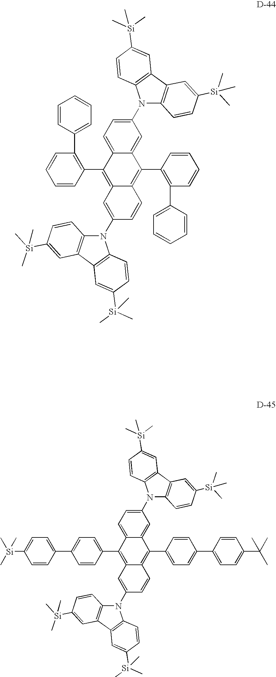


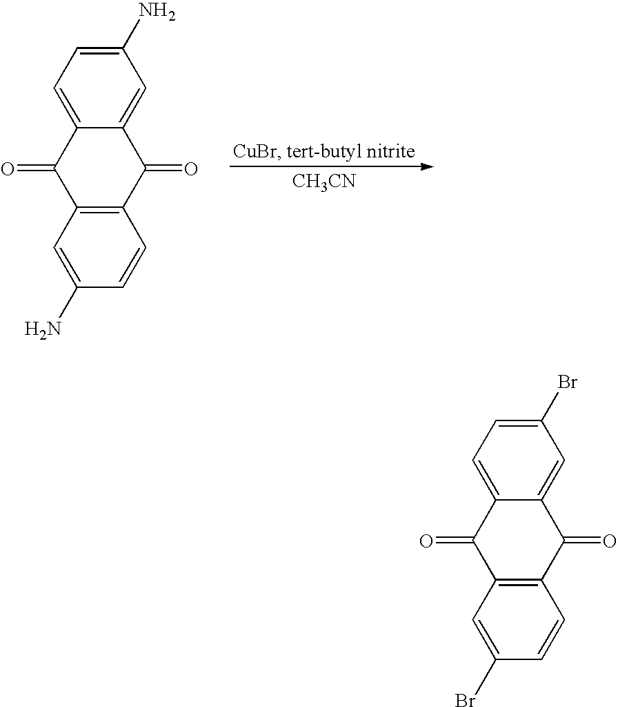


| TABLE 1 | ||||
| Color | ||||
| Current | Power | coordinates | ||
| Current | Luminance | efficiency | efficiency | CIE | CIE | |||
| Voltage (v) | (mA) | (cd/m2) | (cd/A) | (lm/W) | (X) | (Y) | ||
| Example 1 | 5.2 | 0.9 | 779 | 7.8 | 4.74 | 0.137 | 0.177 |
| Example 2 | 5.3 | 0.9 | 730 | 7.3 | 4.32 | 0.129 | 0.163 |
| Example 3 | 5.7 | 0.9 | 848 | 8.5 | 4.67 | 0.137 | 0.187 |
| Example 4 | 5.7 | 0.9 | 896 | 8.9 | 4.93 | 0.138 | 0.193 |
| Example 5 | 5.7 | 0.9 | 778 | 7.8 | 4.28 | 0.136 | 0.195 |
| Comparative | 6.7 | 0.9 | 526 | 5.26 | 2.47 | 0.136 | 0.188 |
| Example 1 | |||||||
Claims (5)


Applications Claiming Priority (2)
| Application Number | Priority Date | Filing Date | Title |
|---|---|---|---|
| KR10-2008-0124243 | 2008-12-08 | ||
| KR1020080124243A KR101507166B1 (en) | 2008-12-08 | 2008-12-08 | Blue light emitting compounds and organic electroluminescent devices containing them |
Publications (2)
| Publication Number | Publication Date |
|---|---|
| US20100140603A1 US20100140603A1 (en) | 2010-06-10 |
| US8299703B2 true US8299703B2 (en) | 2012-10-30 |
Family
ID=42230055
Family Applications (1)
| Application Number | Title | Priority Date | Filing Date |
|---|---|---|---|
| US12/630,589 Active 2030-01-08 US8299703B2 (en) | 2008-12-08 | 2009-12-03 | Blue light emitting compound and organic light emitting diode device comprising the same |
Country Status (4)
| Country | Link |
|---|---|
| US (1) | US8299703B2 (en) |
| KR (1) | KR101507166B1 (en) |
| CN (1) | CN101747256B (en) |
| TW (1) | TWI466979B (en) |
Cited By (1)
| Publication number | Priority date | Publication date | Assignee | Title |
|---|---|---|---|---|
| US12398315B2 (en) | 2018-08-17 | 2025-08-26 | Lg Display Co., Ltd. | Organic electroluminescence device |
Families Citing this family (12)
| Publication number | Priority date | Publication date | Assignee | Title |
|---|---|---|---|---|
| PL2440015T3 (en) | 2009-06-05 | 2018-04-30 | Beijing Visionox Technology Co., Ltd. | Organic electroluminescence device and testing method thereof |
| KR101411122B1 (en) * | 2009-11-13 | 2014-06-25 | 베이징 비젼녹스 테크놀로지 컴퍼니 리미티드 | Organic material and organic EL device using the same material |
| WO2011152466A1 (en) * | 2010-06-02 | 2011-12-08 | Jnc株式会社 | Carbazole compound having substituent group including electron-accepting nitrogen-containing heteroaryl, and organic electroluminescent element |
| CN104744349B (en) * | 2010-11-04 | 2017-09-22 | 捷恩智株式会社 | Electron transport material and use its organic electroluminescent element |
| JP5807601B2 (en) * | 2011-04-01 | 2015-11-10 | Jnc株式会社 | Anthracene derivative and organic electroluminescence device using the same |
| JP5499227B1 (en) * | 2012-08-21 | 2014-05-21 | 保土谷化学工業株式会社 | Compound having triphenylsilylpyridyl group and carbazole ring structure and organic electroluminescence device |
| KR101420527B1 (en) | 2012-11-30 | 2014-07-17 | 인하대학교 산학협력단 | Photoresist Employing Photodimerization Chemistry and Method For Manufacturing Organic Light Emitting Diode Display Using The Same |
| KR102181234B1 (en) * | 2013-08-28 | 2020-11-23 | 삼성디스플레이 주식회사 | Compound and organic light emitting device comprising the same |
| US10403825B2 (en) | 2014-02-27 | 2019-09-03 | Universal Display Corporation | Organic electroluminescent materials and devices |
| US10287398B2 (en) | 2014-12-30 | 2019-05-14 | Momentive Performance Materials Inc. | Siloxane coordination polymers |
| JP2018507280A (en) | 2014-12-30 | 2018-03-15 | モメンティブ パフォーマンス マテリアルズ インコーポレイテッド | Functionalized siloxane materials |
| JP7165943B2 (en) * | 2017-11-01 | 2022-11-07 | 東洋紡株式会社 | Compounds having a π-electron conjugated unit and a carbazole group |
Citations (5)
| Publication number | Priority date | Publication date | Assignee | Title |
|---|---|---|---|---|
| JP2003146951A (en) * | 2001-08-06 | 2003-05-21 | Mitsubishi Chemicals Corp | Anthracene-based compound, method for producing the same, and organic electroluminescent device |
| JP2006248900A (en) | 2005-03-08 | 2006-09-21 | Sony Corp | Anthracene derivative, method for synthesizing anthracene derivative, organic electroluminescent element, and display device |
| JP2007015933A (en) * | 2005-07-05 | 2007-01-25 | Sony Corp | Method for synthesizing anthracene derivative, organic electroluminescent element, and display device |
| KR20090046731A (en) * | 2007-11-05 | 2009-05-11 | 에스에프씨 주식회사 | Anthracene Derivatives and Organic Electroluminescent Devices Employing the Same |
| US20100051106A1 (en) * | 2008-06-25 | 2010-03-04 | Gracel Display Inc. | Novel organic electroluminescent compounds and organic electroluminescent device using the same |
-
2008
- 2008-12-08 KR KR1020080124243A patent/KR101507166B1/en active Active
-
2009
- 2009-11-23 CN CN2009102219332A patent/CN101747256B/en active Active
- 2009-12-03 US US12/630,589 patent/US8299703B2/en active Active
- 2009-12-04 TW TW98141636A patent/TWI466979B/en active
Patent Citations (6)
| Publication number | Priority date | Publication date | Assignee | Title |
|---|---|---|---|---|
| JP2003146951A (en) * | 2001-08-06 | 2003-05-21 | Mitsubishi Chemicals Corp | Anthracene-based compound, method for producing the same, and organic electroluminescent device |
| JP2006248900A (en) | 2005-03-08 | 2006-09-21 | Sony Corp | Anthracene derivative, method for synthesizing anthracene derivative, organic electroluminescent element, and display device |
| JP2007015933A (en) * | 2005-07-05 | 2007-01-25 | Sony Corp | Method for synthesizing anthracene derivative, organic electroluminescent element, and display device |
| KR20090046731A (en) * | 2007-11-05 | 2009-05-11 | 에스에프씨 주식회사 | Anthracene Derivatives and Organic Electroluminescent Devices Employing the Same |
| US20100051106A1 (en) * | 2008-06-25 | 2010-03-04 | Gracel Display Inc. | Novel organic electroluminescent compounds and organic electroluminescent device using the same |
| CN101792422A (en) | 2008-06-25 | 2010-08-04 | 葛来西雅帝史派有限公司 | Novel organic electroluminescent compounds and organic electroluminescent device using the same |
Cited By (1)
| Publication number | Priority date | Publication date | Assignee | Title |
|---|---|---|---|---|
| US12398315B2 (en) | 2018-08-17 | 2025-08-26 | Lg Display Co., Ltd. | Organic electroluminescence device |
Also Published As
| Publication number | Publication date |
|---|---|
| US20100140603A1 (en) | 2010-06-10 |
| TW201022406A (en) | 2010-06-16 |
| CN101747256B (en) | 2012-08-29 |
| KR20100065742A (en) | 2010-06-17 |
| CN101747256A (en) | 2010-06-23 |
| TWI466979B (en) | 2015-01-01 |
| KR101507166B1 (en) | 2015-04-30 |
Similar Documents
| Publication | Publication Date | Title |
|---|---|---|
| US8299703B2 (en) | Blue light emitting compound and organic light emitting diode device comprising the same | |
| US8394511B2 (en) | Compound for forming organic film, and organic light emitting device and flat panel display device including the same | |
| US8541113B2 (en) | Pyrene compounds and organic electroluminescent devices using the same | |
| US7875367B2 (en) | Organoelectroluminescent compound and organoelectroluminescent device employing the same | |
| US8173274B2 (en) | Organic compound and organic electroluminescence device employing the same | |
| US8647753B2 (en) | Organic electroluminescence device | |
| US8835020B2 (en) | Blue fluorescent composition and organic electroluminescent device using the same | |
| US8389131B2 (en) | Material for use in phosphorescent device and organic electroluminescent device using same | |
| US8329953B2 (en) | Cyclopentaphenanthrene-based compound and organic electroluminescent device using the same | |
| US10069073B2 (en) | Organic compounds and organic light emitting device comprising the same | |
| US7854999B2 (en) | Organoelectroluminescent compound and organoelectroluminescent device employing the same | |
| US8298684B2 (en) | Phenylcarbazole compounds, organic light emitting device comprising the phenylcarbazole compounds and flat panel display device comprising the organic light emitting device | |
| US8288014B2 (en) | Fluorene-containing compound and organic light emitting device employing the same | |
| US20170213990A1 (en) | Compound and electronic device including same | |
| US8632893B2 (en) | Organic compound and organic electroluminescence device employing the same | |
| US20100164371A1 (en) | Electron transporting-injection compound and organic electroluminescent device using the same | |
| US9331286B2 (en) | Organic electroluminescent compounds and organic electroluminescent device using the same | |
| US20220271225A1 (en) | Organic electroluminescent compounds and organic electroluminescent device | |
| US20210305514A1 (en) | Polycyclic aromatic compound and organoelectroluminescent device using the same | |
| US20220006013A1 (en) | Organoelectroluminescent device using polycyclic aromatic compounds | |
| US9284486B2 (en) | Blue fluorescent composition and organic electroluminescent device using the same | |
| KR20110065978A (en) | Red phosphorescent host compound and organic light emitting device using the same | |
| US20230371376A1 (en) | Polycyclic compound and organic light-emitting device using same | |
| US12410199B2 (en) | Organic light emitting compound and organic light emitting device | |
| KR102174027B1 (en) | Phosphorescene host compounds and organic light emitting device comprising the same |
Legal Events
| Date | Code | Title | Description |
|---|---|---|---|
| AS | Assignment |
Owner name: LG. DISPLAY CO. LTD.,KOREA, REPUBLIC OF Free format text: ASSIGNMENT OF ASSIGNORS INTEREST;ASSIGNORS:JEONG, HYUNCHEOL;PARK, CHUNGUN;REEL/FRAME:023602/0110 Effective date: 20091201 Owner name: LG. DISPLAY CO. LTD., KOREA, REPUBLIC OF Free format text: ASSIGNMENT OF ASSIGNORS INTEREST;ASSIGNORS:JEONG, HYUNCHEOL;PARK, CHUNGUN;REEL/FRAME:023602/0110 Effective date: 20091201 |
|
| STCF | Information on status: patent grant |
Free format text: PATENTED CASE |
|
| FEPP | Fee payment procedure |
Free format text: PAYOR NUMBER ASSIGNED (ORIGINAL EVENT CODE: ASPN); ENTITY STATUS OF PATENT OWNER: LARGE ENTITY |
|
| FPAY | Fee payment |
Year of fee payment: 4 |
|
| MAFP | Maintenance fee payment |
Free format text: PAYMENT OF MAINTENANCE FEE, 8TH YEAR, LARGE ENTITY (ORIGINAL EVENT CODE: M1552); ENTITY STATUS OF PATENT OWNER: LARGE ENTITY Year of fee payment: 8 |
|
| MAFP | Maintenance fee payment |
Free format text: PAYMENT OF MAINTENANCE FEE, 12TH YEAR, LARGE ENTITY (ORIGINAL EVENT CODE: M1553); ENTITY STATUS OF PATENT OWNER: LARGE ENTITY Year of fee payment: 12 |