US10069073B2 - Organic compounds and organic light emitting device comprising the same - Google Patents
Organic compounds and organic light emitting device comprising the same Download PDFInfo
- Publication number
- US10069073B2 US10069073B2 US14/553,601 US201414553601A US10069073B2 US 10069073 B2 US10069073 B2 US 10069073B2 US 201414553601 A US201414553601 A US 201414553601A US 10069073 B2 US10069073 B2 US 10069073B2
- Authority
- US
- United States
- Prior art keywords
- layer
- light emitting
- group
- organic compound
- substituted
- Prior art date
- Legal status (The legal status is an assumption and is not a legal conclusion. Google has not performed a legal analysis and makes no representation as to the accuracy of the status listed.)
- Active, expires
Links
- 150000002894 organic compounds Chemical class 0.000 title claims abstract description 85
- 239000000126 substance Substances 0.000 claims abstract description 10
- 150000001875 compounds Chemical class 0.000 claims description 70
- 238000002347 injection Methods 0.000 claims description 62
- 239000007924 injection Substances 0.000 claims description 62
- 230000005525 hole transport Effects 0.000 claims description 54
- 239000000463 material Substances 0.000 claims description 48
- 125000003277 amino group Chemical group 0.000 claims description 24
- 239000000872 buffer Substances 0.000 claims description 24
- 125000003118 aryl group Chemical group 0.000 claims description 23
- 125000001072 heteroaryl group Chemical group 0.000 claims description 23
- 125000003709 fluoroalkyl group Chemical group 0.000 claims description 14
- 229910052805 deuterium Inorganic materials 0.000 claims description 12
- 125000004431 deuterium atom Chemical group 0.000 claims description 12
- 125000005843 halogen group Chemical group 0.000 claims description 12
- 125000004435 hydrogen atom Chemical group [H]* 0.000 claims description 12
- 125000000217 alkyl group Chemical group 0.000 claims description 11
- -1 —OH Chemical group 0.000 claims description 11
- 125000003545 alkoxy group Chemical group 0.000 claims description 10
- 125000004104 aryloxy group Chemical group 0.000 claims description 10
- 125000002915 carbonyl group Chemical group [*:2]C([*:1])=O 0.000 claims description 10
- 125000003178 carboxy group Chemical group [H]OC(*)=O 0.000 claims description 10
- 125000005553 heteroaryloxy group Chemical group 0.000 claims description 10
- 125000003808 silyl group Chemical group [H][Si]([H])([H])[*] 0.000 claims description 4
- 150000004057 1,4-benzoquinones Chemical class 0.000 claims description 2
- 125000001424 substituent group Chemical group 0.000 claims description 2
- 239000010410 layer Substances 0.000 description 164
- YMWUJEATGCHHMB-UHFFFAOYSA-N Dichloromethane Chemical compound ClCCl YMWUJEATGCHHMB-UHFFFAOYSA-N 0.000 description 129
- VLKZOEOYAKHREP-UHFFFAOYSA-N n-Hexane Chemical compound CCCCCC VLKZOEOYAKHREP-UHFFFAOYSA-N 0.000 description 32
- XLYOFNOQVPJJNP-UHFFFAOYSA-N water Chemical compound O XLYOFNOQVPJJNP-UHFFFAOYSA-N 0.000 description 32
- XEKOWRVHYACXOJ-UHFFFAOYSA-N Ethyl acetate Chemical compound CCOC(C)=O XEKOWRVHYACXOJ-UHFFFAOYSA-N 0.000 description 24
- 230000000052 comparative effect Effects 0.000 description 19
- JUJWROOIHBZHMG-UHFFFAOYSA-N Pyridine Chemical compound C1=CC=NC=C1 JUJWROOIHBZHMG-UHFFFAOYSA-N 0.000 description 18
- 238000006243 chemical reaction Methods 0.000 description 18
- 238000002360 preparation method Methods 0.000 description 18
- RTZKZFJDLAIYFH-UHFFFAOYSA-N Diethyl ether Chemical compound CCOCC RTZKZFJDLAIYFH-UHFFFAOYSA-N 0.000 description 16
- 239000000203 mixture Substances 0.000 description 14
- BWHMMNNQKKPAPP-UHFFFAOYSA-L potassium carbonate Chemical compound [K+].[K+].[O-]C([O-])=O BWHMMNNQKKPAPP-UHFFFAOYSA-L 0.000 description 14
- QTBSBXVTEAMEQO-UHFFFAOYSA-N Acetic acid Chemical compound CC(O)=O QTBSBXVTEAMEQO-UHFFFAOYSA-N 0.000 description 12
- 239000012153 distilled water Substances 0.000 description 11
- 239000007788 liquid Substances 0.000 description 11
- 0 *C1=C([1*])C(=C)C([4*])=C([3*])C1=[Y] Chemical compound *C1=C([1*])C(=C)C([4*])=C([3*])C1=[Y] 0.000 description 10
- NFHFRUOZVGFOOS-UHFFFAOYSA-N palladium;triphenylphosphane Chemical compound [Pd].C1=CC=CC=C1P(C=1C=CC=CC=1)C1=CC=CC=C1.C1=CC=CC=C1P(C=1C=CC=CC=1)C1=CC=CC=C1.C1=CC=CC=C1P(C=1C=CC=CC=1)C1=CC=CC=C1.C1=CC=CC=C1P(C=1C=CC=CC=1)C1=CC=CC=C1 NFHFRUOZVGFOOS-UHFFFAOYSA-N 0.000 description 10
- ZMXDDKWLCZADIW-UHFFFAOYSA-N N,N-Dimethylformamide Chemical compound CN(C)C=O ZMXDDKWLCZADIW-UHFFFAOYSA-N 0.000 description 9
- 239000002019 doping agent Substances 0.000 description 9
- 238000000034 method Methods 0.000 description 9
- UMJSCPRVCHMLSP-UHFFFAOYSA-N pyridine Natural products COC1=CC=CN=C1 UMJSCPRVCHMLSP-UHFFFAOYSA-N 0.000 description 9
- XJDNKRIXUMDJCW-UHFFFAOYSA-J titanium tetrachloride Chemical compound Cl[Ti](Cl)(Cl)Cl XJDNKRIXUMDJCW-UHFFFAOYSA-J 0.000 description 9
- 239000003208 petroleum Substances 0.000 description 8
- 238000001556 precipitation Methods 0.000 description 8
- 238000000926 separation method Methods 0.000 description 8
- 229910000027 potassium carbonate Inorganic materials 0.000 description 7
- HEDRZPFGACZZDS-UHFFFAOYSA-N Chloroform Chemical compound ClC(Cl)Cl HEDRZPFGACZZDS-UHFFFAOYSA-N 0.000 description 6
- 229910052782 aluminium Inorganic materials 0.000 description 6
- XAGFODPZIPBFFR-UHFFFAOYSA-N aluminium Chemical compound [Al] XAGFODPZIPBFFR-UHFFFAOYSA-N 0.000 description 6
- 238000004440 column chromatography Methods 0.000 description 6
- 239000011259 mixed solution Substances 0.000 description 5
- QAOWNCQODCNURD-UHFFFAOYSA-N Sulfuric acid Chemical compound OS(O)(=O)=O QAOWNCQODCNURD-UHFFFAOYSA-N 0.000 description 4
- 239000011575 calcium Substances 0.000 description 4
- 230000006866 deterioration Effects 0.000 description 4
- 239000011777 magnesium Substances 0.000 description 4
- 238000004519 manufacturing process Methods 0.000 description 4
- TVIVIEFSHFOWTE-UHFFFAOYSA-K tri(quinolin-8-yloxy)alumane Chemical compound [Al+3].C1=CN=C2C([O-])=CC=CC2=C1.C1=CN=C2C([O-])=CC=CC2=C1.C1=CN=C2C([O-])=CC=CC2=C1 TVIVIEFSHFOWTE-UHFFFAOYSA-K 0.000 description 4
- 238000010626 work up procedure Methods 0.000 description 4
- 229940126062 Compound A Drugs 0.000 description 3
- NLDMNSXOCDLTTB-UHFFFAOYSA-N Heterophylliin A Natural products O1C2COC(=O)C3=CC(O)=C(O)C(O)=C3C3=C(O)C(O)=C(O)C=C3C(=O)OC2C(OC(=O)C=2C=C(O)C(O)=C(O)C=2)C(O)C1OC(=O)C1=CC(O)=C(O)C(O)=C1 NLDMNSXOCDLTTB-UHFFFAOYSA-N 0.000 description 3
- PXHVJJICTQNCMI-UHFFFAOYSA-N Nickel Chemical compound [Ni] PXHVJJICTQNCMI-UHFFFAOYSA-N 0.000 description 3
- WYURNTSHIVDZCO-UHFFFAOYSA-N Tetrahydrofuran Chemical compound C1CCOC1 WYURNTSHIVDZCO-UHFFFAOYSA-N 0.000 description 3
- 239000007983 Tris buffer Substances 0.000 description 3
- XLOMVQKBTHCTTD-UHFFFAOYSA-N Zinc monoxide Chemical compound [Zn]=O XLOMVQKBTHCTTD-UHFFFAOYSA-N 0.000 description 3
- 229910052791 calcium Inorganic materials 0.000 description 3
- 238000011161 development Methods 0.000 description 3
- 229910052749 magnesium Inorganic materials 0.000 description 3
- 229910052751 metal Inorganic materials 0.000 description 3
- 239000002184 metal Substances 0.000 description 3
- 150000002736 metal compounds Chemical class 0.000 description 3
- 238000012986 modification Methods 0.000 description 3
- 230000004048 modification Effects 0.000 description 3
- 239000011368 organic material Substances 0.000 description 3
- 229920000767 polyaniline Polymers 0.000 description 3
- 239000000758 substrate Substances 0.000 description 3
- POILWHVDKZOXJZ-ARJAWSKDSA-M (z)-4-oxopent-2-en-2-olate Chemical compound C\C([O-])=C\C(C)=O POILWHVDKZOXJZ-ARJAWSKDSA-M 0.000 description 2
- NGQSLSMAEVWNPU-YTEMWHBBSA-N 1,2-bis[(e)-2-phenylethenyl]benzene Chemical compound C=1C=CC=CC=1/C=C/C1=CC=CC=C1\C=C\C1=CC=CC=C1 NGQSLSMAEVWNPU-YTEMWHBBSA-N 0.000 description 2
- RYHBNJHYFVUHQT-UHFFFAOYSA-N 1,4-Dioxane Chemical compound C1COCCO1 RYHBNJHYFVUHQT-UHFFFAOYSA-N 0.000 description 2
- IXHWGNYCZPISET-UHFFFAOYSA-N 2-[4-(dicyanomethylidene)-2,3,5,6-tetrafluorocyclohexa-2,5-dien-1-ylidene]propanedinitrile Chemical compound FC1=C(F)C(=C(C#N)C#N)C(F)=C(F)C1=C(C#N)C#N IXHWGNYCZPISET-UHFFFAOYSA-N 0.000 description 2
- PYEQXZOIQJWYAH-UHFFFAOYSA-N 2-bromocyclohexa-2,5-diene-1,4-dione Chemical compound BrC1=CC(=O)C=CC1=O PYEQXZOIQJWYAH-UHFFFAOYSA-N 0.000 description 2
- 229910052693 Europium Inorganic materials 0.000 description 2
- CSNNHWWHGAXBCP-UHFFFAOYSA-L Magnesium sulfate Chemical compound [Mg+2].[O-][S+2]([O-])([O-])[O-] CSNNHWWHGAXBCP-UHFFFAOYSA-L 0.000 description 2
- OAICVXFJPJFONN-UHFFFAOYSA-N Phosphorus Chemical compound [P] OAICVXFJPJFONN-UHFFFAOYSA-N 0.000 description 2
- BQCADISMDOOEFD-UHFFFAOYSA-N Silver Chemical compound [Ag] BQCADISMDOOEFD-UHFFFAOYSA-N 0.000 description 2
- 229910052769 Ytterbium Inorganic materials 0.000 description 2
- CUJRVFIICFDLGR-UHFFFAOYSA-N acetylacetonate Chemical compound CC(=O)[CH-]C(C)=O CUJRVFIICFDLGR-UHFFFAOYSA-N 0.000 description 2
- 229910052784 alkaline earth metal Inorganic materials 0.000 description 2
- 150000004984 aromatic diamines Chemical class 0.000 description 2
- UFVXQDWNSAGPHN-UHFFFAOYSA-K bis[(2-methylquinolin-8-yl)oxy]-(4-phenylphenoxy)alumane Chemical compound [Al+3].C1=CC=C([O-])C2=NC(C)=CC=C21.C1=CC=C([O-])C2=NC(C)=CC=C21.C1=CC([O-])=CC=C1C1=CC=CC=C1 UFVXQDWNSAGPHN-UHFFFAOYSA-K 0.000 description 2
- 229910052792 caesium Inorganic materials 0.000 description 2
- DKHNGUNXLDCATP-UHFFFAOYSA-N dipyrazino[2,3-f:2',3'-h]quinoxaline-2,3,6,7,10,11-hexacarbonitrile Chemical compound C12=NC(C#N)=C(C#N)N=C2C2=NC(C#N)=C(C#N)N=C2C2=C1N=C(C#N)C(C#N)=N2 DKHNGUNXLDCATP-UHFFFAOYSA-N 0.000 description 2
- 238000009826 distribution Methods 0.000 description 2
- 229910052741 iridium Inorganic materials 0.000 description 2
- GKOZUEZYRPOHIO-UHFFFAOYSA-N iridium atom Chemical compound [Ir] GKOZUEZYRPOHIO-UHFFFAOYSA-N 0.000 description 2
- UEEXRMUCXBPYOV-UHFFFAOYSA-N iridium;2-phenylpyridine Chemical compound [Ir].C1=CC=CC=C1C1=CC=CC=N1.C1=CC=CC=C1C1=CC=CC=N1.C1=CC=CC=C1C1=CC=CC=N1 UEEXRMUCXBPYOV-UHFFFAOYSA-N 0.000 description 2
- CUONGYYJJVDODC-UHFFFAOYSA-N malononitrile Chemical compound N#CCC#N CUONGYYJJVDODC-UHFFFAOYSA-N 0.000 description 2
- IBHBKWKFFTZAHE-UHFFFAOYSA-N n-[4-[4-(n-naphthalen-1-ylanilino)phenyl]phenyl]-n-phenylnaphthalen-1-amine Chemical compound C1=CC=CC=C1N(C=1C2=CC=CC=C2C=CC=1)C1=CC=C(C=2C=CC(=CC=2)N(C=2C=CC=CC=2)C=2C3=CC=CC=C3C=CC=2)C=C1 IBHBKWKFFTZAHE-UHFFFAOYSA-N 0.000 description 2
- 229910052698 phosphorus Inorganic materials 0.000 description 2
- 239000011574 phosphorus Substances 0.000 description 2
- IEQIEDJGQAUEQZ-UHFFFAOYSA-N phthalocyanine Chemical compound N1C(N=C2C3=CC=CC=C3C(N=C3C4=CC=CC=C4C(=N4)N3)=N2)=C(C=CC=C2)C2=C1N=C1C2=CC=CC=C2C4=N1 IEQIEDJGQAUEQZ-UHFFFAOYSA-N 0.000 description 2
- 229920000642 polymer Polymers 0.000 description 2
- 229910052700 potassium Inorganic materials 0.000 description 2
- 229910052701 rubidium Inorganic materials 0.000 description 2
- 229910052709 silver Inorganic materials 0.000 description 2
- 239000004332 silver Substances 0.000 description 2
- 239000002356 single layer Substances 0.000 description 2
- 229910052708 sodium Inorganic materials 0.000 description 2
- 239000011734 sodium Substances 0.000 description 2
- 238000003756 stirring Methods 0.000 description 2
- 229910052712 strontium Inorganic materials 0.000 description 2
- ZSYMVHGRKPBJCQ-UHFFFAOYSA-N 1,1'-biphenyl;9h-carbazole Chemical group C1=CC=CC=C1C1=CC=CC=C1.C1=CC=C2C3=CC=CC=C3NC2=C1 ZSYMVHGRKPBJCQ-UHFFFAOYSA-N 0.000 description 1
- JYEUMXHLPRZUAT-UHFFFAOYSA-N 1,2,3-triazine Chemical compound C1=CN=NN=C1 JYEUMXHLPRZUAT-UHFFFAOYSA-N 0.000 description 1
- SPDPTFAJSFKAMT-UHFFFAOYSA-N 1-n-[4-[4-(n-[4-(3-methyl-n-(3-methylphenyl)anilino)phenyl]anilino)phenyl]phenyl]-4-n,4-n-bis(3-methylphenyl)-1-n-phenylbenzene-1,4-diamine Chemical compound CC1=CC=CC(N(C=2C=CC(=CC=2)N(C=2C=CC=CC=2)C=2C=CC(=CC=2)C=2C=CC(=CC=2)N(C=2C=CC=CC=2)C=2C=CC(=CC=2)N(C=2C=C(C)C=CC=2)C=2C=C(C)C=CC=2)C=2C=C(C)C=CC=2)=C1 SPDPTFAJSFKAMT-UHFFFAOYSA-N 0.000 description 1
- VBQVHWHWZOUENI-UHFFFAOYSA-N 1-phenyl-2H-quinoline Chemical compound C1C=CC2=CC=CC=C2N1C1=CC=CC=C1 VBQVHWHWZOUENI-UHFFFAOYSA-N 0.000 description 1
- LPCWDYWZIWDTCV-UHFFFAOYSA-N 1-phenylisoquinoline Chemical compound C1=CC=CC=C1C1=NC=CC2=CC=CC=C12 LPCWDYWZIWDTCV-UHFFFAOYSA-N 0.000 description 1
- YXWJGZQOGXGSSC-UHFFFAOYSA-N 2,3,4,5,6-pentafluorobenzonitrile Chemical compound FC1=C(F)C(F)=C(C#N)C(F)=C1F YXWJGZQOGXGSSC-UHFFFAOYSA-N 0.000 description 1
- UOXJNGFFPMOZDM-UHFFFAOYSA-N 2-[di(propan-2-yl)amino]ethylsulfanyl-methylphosphinic acid Chemical compound CC(C)N(C(C)C)CCSP(C)(O)=O UOXJNGFFPMOZDM-UHFFFAOYSA-N 0.000 description 1
- HNWFFTUWRIGBNM-UHFFFAOYSA-N 2-methyl-9,10-dinaphthalen-2-ylanthracene Chemical compound C1=CC=CC2=CC(C3=C4C=CC=CC4=C(C=4C=C5C=CC=CC5=CC=4)C4=CC=C(C=C43)C)=CC=C21 HNWFFTUWRIGBNM-UHFFFAOYSA-N 0.000 description 1
- DIVZFUBWFAOMCW-UHFFFAOYSA-N 4-n-(3-methylphenyl)-1-n,1-n-bis[4-(n-(3-methylphenyl)anilino)phenyl]-4-n-phenylbenzene-1,4-diamine Chemical compound CC1=CC=CC(N(C=2C=CC=CC=2)C=2C=CC(=CC=2)N(C=2C=CC(=CC=2)N(C=2C=CC=CC=2)C=2C=C(C)C=CC=2)C=2C=CC(=CC=2)N(C=2C=CC=CC=2)C=2C=C(C)C=CC=2)=C1 DIVZFUBWFAOMCW-UHFFFAOYSA-N 0.000 description 1
- SFHYNDMGZXWXBU-LIMNOBDPSA-N 6-amino-2-[[(e)-(3-formylphenyl)methylideneamino]carbamoylamino]-1,3-dioxobenzo[de]isoquinoline-5,8-disulfonic acid Chemical compound O=C1C(C2=3)=CC(S(O)(=O)=O)=CC=3C(N)=C(S(O)(=O)=O)C=C2C(=O)N1NC(=O)N\N=C\C1=CC=CC(C=O)=C1 SFHYNDMGZXWXBU-LIMNOBDPSA-N 0.000 description 1
- VFUDMQLBKNMONU-UHFFFAOYSA-N 9-[4-(4-carbazol-9-ylphenyl)phenyl]carbazole Chemical group C12=CC=CC=C2C2=CC=CC=C2N1C1=CC=C(C=2C=CC(=CC=2)N2C3=CC=CC=C3C3=CC=CC=C32)C=C1 VFUDMQLBKNMONU-UHFFFAOYSA-N 0.000 description 1
- LCZJJWGIOSMIND-UHFFFAOYSA-N B.BB.BBB.CC1=CC(C(F)(F)F)=CC(B(O)O)=C1.CC1=CC(C2=CC(=O)C(C3=CC(C(F)(F)F)=CC(C(F)(F)F)=C3)=CC2=O)=CC(C(F)(F)F)=C1.O=C1C=C(Br)C(=O)C=C1Br Chemical compound B.BB.BBB.CC1=CC(C(F)(F)F)=CC(B(O)O)=C1.CC1=CC(C2=CC(=O)C(C3=CC(C(F)(F)F)=CC(C(F)(F)F)=C3)=CC2=O)=CC(C(F)(F)F)=C1.O=C1C=C(Br)C(=O)C=C1Br LCZJJWGIOSMIND-UHFFFAOYSA-N 0.000 description 1
- PIKYKZDNDMNOJY-XMPJSRFYSA-J BB(B)B.BBB.BBB(B)B.CC1=CC(C2=CC(=O)C(C3=CC(C(F)(F)F)=CC(C(F)(F)F)=C3)=CC2=O)=CC(C(F)(F)F)=C1.Cl[Ti](Cl)(Cl)Cl.[C-]#[N+]/C(C#N)=C1/C=C(C2=CC(C(F)(F)F)=CC(C(F)(F)F)=C2)/C(=C(\C#N)[N+]#[C-])C=C1C1=CC(C(F)(F)F)=CC(C)=C1.[C-]#[N+]CC#N Chemical compound BB(B)B.BBB.BBB(B)B.CC1=CC(C2=CC(=O)C(C3=CC(C(F)(F)F)=CC(C(F)(F)F)=C3)=CC2=O)=CC(C(F)(F)F)=C1.Cl[Ti](Cl)(Cl)Cl.[C-]#[N+]/C(C#N)=C1/C=C(C2=CC(C(F)(F)F)=CC(C(F)(F)F)=C2)/C(=C(\C#N)[N+]#[C-])C=C1C1=CC(C(F)(F)F)=CC(C)=C1.[C-]#[N+]CC#N PIKYKZDNDMNOJY-XMPJSRFYSA-J 0.000 description 1
- ZZQRDQHVHDPPCW-DFRCKUKFSA-J BB(B)B.BBB.Cl[Ti](Cl)(Cl)Cl.[2HH].[2H][2H].[2H][2H].[C-]#[N+]C1=C(F)C=C(C2=C/C(=C(/C#N)[N+]#[C-])C(C3=CC(F)=C(C#N)C=C3)=CC2=O)C=C1.[C-]#[N+]C1=C(F)C=C(C2=CC(=O)C(C3=CC(F)=C(C#N)C=C3)=CC2=O)C=C1.[C-]#[N+]CC#N Chemical compound BB(B)B.BBB.Cl[Ti](Cl)(Cl)Cl.[2HH].[2H][2H].[2H][2H].[C-]#[N+]C1=C(F)C=C(C2=C/C(=C(/C#N)[N+]#[C-])C(C3=CC(F)=C(C#N)C=C3)=CC2=O)C=C1.[C-]#[N+]C1=C(F)C=C(C2=CC(=O)C(C3=CC(F)=C(C#N)C=C3)=CC2=O)C=C1.[C-]#[N+]CC#N ZZQRDQHVHDPPCW-DFRCKUKFSA-J 0.000 description 1
- MYXIBTHHTPBPKP-PFQDNATASA-J C#CC.C#CC#CC.CC#CC.Cl[Ti](Cl)(Cl)Cl.[C-]#[N+]C1=C(F)C=C(C2=C/C(=C(/C#N)[N+]#[C-])C(C3=CC(F)=C(C#N)C=C3)=C/C2=C(\C#N)[N+]#[C-])C=C1.[C-]#[N+]C1=C(F)C=C(C2=CC(=O)C(C3=CC(F)=C(C#N)C=C3)=CC2=O)C=C1.[C-]#[N+]CC#N Chemical compound C#CC.C#CC#CC.CC#CC.Cl[Ti](Cl)(Cl)Cl.[C-]#[N+]C1=C(F)C=C(C2=C/C(=C(/C#N)[N+]#[C-])C(C3=CC(F)=C(C#N)C=C3)=C/C2=C(\C#N)[N+]#[C-])C=C1.[C-]#[N+]C1=C(F)C=C(C2=CC(=O)C(C3=CC(F)=C(C#N)C=C3)=CC2=O)C=C1.[C-]#[N+]CC#N MYXIBTHHTPBPKP-PFQDNATASA-J 0.000 description 1
- MTNUHQDTKTXMGR-UHFFFAOYSA-N C.C#C.C#CC.O=C1C=C(Br)C(=O)C=C1Br.[C-]#[N+]C1=CC=C(B(O)O)C=C1F.[C-]#[N+]C1=CC=C(C2=CC(=O)C(C3=CC=C(C#N)C(F)=C3)=CC2=O)C=C1F Chemical compound C.C#C.C#CC.O=C1C=C(Br)C(=O)C=C1Br.[C-]#[N+]C1=CC=C(B(O)O)C=C1F.[C-]#[N+]C1=CC=C(C2=CC(=O)C(C3=CC=C(C#N)C(F)=C3)=CC2=O)C=C1F MTNUHQDTKTXMGR-UHFFFAOYSA-N 0.000 description 1
- VESLADIKDWLYQJ-UHFFFAOYSA-N C.C.C.CC1=CC=C(B(O)O)C=C1.CC1=CC=C(C2=CC(=O)C(C3=CC=C(C(F)(F)F)C=C3)=CC2=O)C=C1.O=C1C=C(Br)C(=O)C=C1Br Chemical compound C.C.C.CC1=CC=C(B(O)O)C=C1.CC1=CC=C(C2=CC(=O)C(C3=CC=C(C(F)(F)F)C=C3)=CC2=O)C=C1.O=C1C=C(Br)C(=O)C=C1Br VESLADIKDWLYQJ-UHFFFAOYSA-N 0.000 description 1
- HSCLWBFUBGQLCG-XMPJSRFYSA-J C.C.C.CC1=CC=C(C2=CC(=O)C(C3=CC=C(C(F)(F)F)C=C3)=CC2=O)C=C1.Cl[Ti](Cl)(Cl)Cl.[C-]#[N+]/C(C#N)=C1/C=C(C2=CC=C(C(F)(F)F)C=C2)/C(=C(\C#N)[N+]#[C-])C=C1C1=CC=C(C)C=C1.[C-]#[N+]CC#N Chemical compound C.C.C.CC1=CC=C(C2=CC(=O)C(C3=CC=C(C(F)(F)F)C=C3)=CC2=O)C=C1.Cl[Ti](Cl)(Cl)Cl.[C-]#[N+]/C(C#N)=C1/C=C(C2=CC=C(C(F)(F)F)C=C2)/C(=C(\C#N)[N+]#[C-])C=C1C1=CC=C(C)C=C1.[C-]#[N+]CC#N HSCLWBFUBGQLCG-XMPJSRFYSA-J 0.000 description 1
- FESNZYWYVVSSKR-IEOGHOGCSA-N C/C(C1=C(F)C(F)=C(F)C(F)=C1F)=C1/C=C(C2=C(F)C(F)=C(F)C(F)=C2F)/C(=C(/C2=C(F)C(F)=C(F)C(F)=C2F)C(F)(F)F)C=C1C1=C(F)C(F)=C(F)C(F)=C1F.CC1=CC(C2=C/C(=C(\C3=CC(C)=CC(C(F)(F)F)=C3)C(F)(F)F)C(C3=CC(C(F)(F)F)=CC(C(F)(F)F)=C3)=C/C2=C(/C)C2=CC(C(F)(F)F)=CC(C(F)(F)F)=C2)=CC(C(F)(F)F)=C1.[C-]#[N+]C1=CC(C2=C/C(=C(/C#N)C3=C(C(F)(F)F)C=C(C)C=C3C(F)(F)F)C(C3=CC=C(F)C(C#N)=C3)=C/C2=C(/[N+]#[C-])C2=C(C(F)(F)F)C=C(C(F)(F)F)C=C2C)=CC=C1F.[C-]#[N+]C1=CC(C2=C/C(=C(\C3=C(F)C(F)=C([N+]#[C-])C(F)=C3F)C(F)(F)F)C(C3=CC(C#N)=CC(C#N)=C3)=C/C2=C(/C)C2=C(F)C(F)=C(C#N)C(F)=C2F)=CC(C#N)=C1 Chemical compound C/C(C1=C(F)C(F)=C(F)C(F)=C1F)=C1/C=C(C2=C(F)C(F)=C(F)C(F)=C2F)/C(=C(/C2=C(F)C(F)=C(F)C(F)=C2F)C(F)(F)F)C=C1C1=C(F)C(F)=C(F)C(F)=C1F.CC1=CC(C2=C/C(=C(\C3=CC(C)=CC(C(F)(F)F)=C3)C(F)(F)F)C(C3=CC(C(F)(F)F)=CC(C(F)(F)F)=C3)=C/C2=C(/C)C2=CC(C(F)(F)F)=CC(C(F)(F)F)=C2)=CC(C(F)(F)F)=C1.[C-]#[N+]C1=CC(C2=C/C(=C(/C#N)C3=C(C(F)(F)F)C=C(C)C=C3C(F)(F)F)C(C3=CC=C(F)C(C#N)=C3)=C/C2=C(/[N+]#[C-])C2=C(C(F)(F)F)C=C(C(F)(F)F)C=C2C)=CC=C1F.[C-]#[N+]C1=CC(C2=C/C(=C(\C3=C(F)C(F)=C([N+]#[C-])C(F)=C3F)C(F)(F)F)C(C3=CC(C#N)=CC(C#N)=C3)=C/C2=C(/C)C2=C(F)C(F)=C(C#N)C(F)=C2F)=CC(C#N)=C1 FESNZYWYVVSSKR-IEOGHOGCSA-N 0.000 description 1
- CETCWYNHJWFAMA-YKGPXHCOSA-K C1=CC2=C3C(=C1)O[Al]14(OC5=CC=CC6=C5/N1=C\C=C/6)(O/C1=C/C=C\C5=C1N4=CC=C5)N3=CC=C2.C1=CC=C(N(C2=CC=C(C3=CC=C(N(C4=CC=CC=C4)C4=C5C=CC=CC5=CC=C4)C=C3)C=C2)C2=CC=CC3=C2C=CC=C3)C=C1.C1=CC=C(N(C2=CC=CC=C2)C2=CC=C3C=CC4=C(N(C5=CC=CC=C5)C5=CC=CC=C5)C=C/C5=C/C=C/2C3=C45)C=C1.CC1=CC2=C(C3=CC4=C(C=CC=C4)C=C3)C3=CC=CC=C3C(C3=CC4=C(C=CC=C4)C=C3)=C2C=C1.[2H-]B Chemical compound C1=CC2=C3C(=C1)O[Al]14(OC5=CC=CC6=C5/N1=C\C=C/6)(O/C1=C/C=C\C5=C1N4=CC=C5)N3=CC=C2.C1=CC=C(N(C2=CC=C(C3=CC=C(N(C4=CC=CC=C4)C4=C5C=CC=CC5=CC=C4)C=C3)C=C2)C2=CC=CC3=C2C=CC=C3)C=C1.C1=CC=C(N(C2=CC=CC=C2)C2=CC=C3C=CC4=C(N(C5=CC=CC=C5)C5=CC=CC=C5)C=C/C5=C/C=C/2C3=C45)C=C1.CC1=CC2=C(C3=CC4=C(C=CC=C4)C=C3)C3=CC=CC=C3C(C3=CC4=C(C=CC=C4)C=C3)=C2C=C1.[2H-]B CETCWYNHJWFAMA-YKGPXHCOSA-K 0.000 description 1
- FDEITQSPFGFRCS-UHFFFAOYSA-N C=C.C=NC Chemical compound C=C.C=NC FDEITQSPFGFRCS-UHFFFAOYSA-N 0.000 description 1
- CUCQRGLOGXNZOG-UHFFFAOYSA-N CC(C)=C(C)C.CC(C)=O.CC(C)=S.CN=C(C)C Chemical compound CC(C)=C(C)C.CC(C)=O.CC(C)=S.CN=C(C)C CUCQRGLOGXNZOG-UHFFFAOYSA-N 0.000 description 1
- MPFHWMRJKDLWHZ-UHFFFAOYSA-N CC1=CC=C(B(O)O)C(C(F)(F)F)=C1.O=C1C=CC(=O)C(Br)=C1.O=C1C=CC(=O)C(C2=CC=C(C(F)(F)F)C=C2C(F)(F)F)=C1 Chemical compound CC1=CC=C(B(O)O)C(C(F)(F)F)=C1.O=C1C=CC(=O)C(Br)=C1.O=C1C=CC(=O)C(C2=CC=C(C(F)(F)F)C=C2C(F)(F)F)=C1 MPFHWMRJKDLWHZ-UHFFFAOYSA-N 0.000 description 1
- GYUFXODNWYCEEX-UHFFFAOYSA-N CC1=CC=C(B(O)O)C=C1.O=C1C=CC(=O)C(Br)=C1.O=C1C=CC(=O)C(C2=CC=C(C(F)(F)F)C=C2)=C1 Chemical compound CC1=CC=C(B(O)O)C=C1.O=C1C=CC(=O)C(Br)=C1.O=C1C=CC(=O)C(C2=CC=C(C(F)(F)F)C=C2)=C1 GYUFXODNWYCEEX-UHFFFAOYSA-N 0.000 description 1
- OYPRJOBELJOOCE-UHFFFAOYSA-N Calcium Chemical compound [Ca] OYPRJOBELJOOCE-UHFFFAOYSA-N 0.000 description 1
- 229910052684 Cerium Inorganic materials 0.000 description 1
- TYHQFYBYZKKADM-CWXYOZBBSA-J Cl[Ti](Cl)(Cl)Cl.F.[C-]#[N+]/C(C#N)=C1\C=CC(=O)C(C2=CC=C(C(F)(F)F)C=C2)=C1.[C-]#[N+]C1=C(F)C(F)=C(/C(C#N)=C2\C=C/C(=C(/C#N)[N+]#[C-])C=C2C2=CC=C(C(F)(F)F)C=C2)C(F)=C1F.[C-]#[N+]C1=C(F)C(F)=C(CC#N)C(C)=C1F Chemical compound Cl[Ti](Cl)(Cl)Cl.F.[C-]#[N+]/C(C#N)=C1\C=CC(=O)C(C2=CC=C(C(F)(F)F)C=C2)=C1.[C-]#[N+]C1=C(F)C(F)=C(/C(C#N)=C2\C=C/C(=C(/C#N)[N+]#[C-])C=C2C2=CC=C(C(F)(F)F)C=C2)C(F)=C1F.[C-]#[N+]C1=C(F)C(F)=C(CC#N)C(C)=C1F TYHQFYBYZKKADM-CWXYOZBBSA-J 0.000 description 1
- AJNLPMUZGNSISI-BJQGMOKZSA-J Cl[Ti](Cl)(Cl)Cl.F.[C-]#[N+]/C(C#N)=C1\C=CC(=O)C(C2=CC=C(C(F)(F)F)C=C2C(F)(F)F)=C1.[C-]#[N+]C1=C(F)C(F)=C(/C(C#N)=C2\C=C/C(=C(/C#N)[N+]#[C-])C=C2C2=CC=C(C(F)(F)F)C=C2C(F)(F)F)C(F)=C1F.[C-]#[N+]C1=C(F)C(F)=C(CC#N)C(C)=C1F Chemical compound Cl[Ti](Cl)(Cl)Cl.F.[C-]#[N+]/C(C#N)=C1\C=CC(=O)C(C2=CC=C(C(F)(F)F)C=C2C(F)(F)F)=C1.[C-]#[N+]C1=C(F)C(F)=C(/C(C#N)=C2\C=C/C(=C(/C#N)[N+]#[C-])C=C2C2=CC=C(C(F)(F)F)C=C2C(F)(F)F)C(F)=C1F.[C-]#[N+]C1=C(F)C(F)=C(CC#N)C(C)=C1F AJNLPMUZGNSISI-BJQGMOKZSA-J 0.000 description 1
- MDDWWJGDZTWGOZ-PZHZLCPESA-J Cl[Ti](Cl)(Cl)Cl.O=C1C=CC(=O)C(C2=CC=C(C(F)(F)F)C=C2)=C1.[C-]#[N+]/C(C#N)=C1\C=CC(=O)C(C2=CC=C(C(F)(F)F)C=C2)=C1.[C-]#[N+]CC#N Chemical compound Cl[Ti](Cl)(Cl)Cl.O=C1C=CC(=O)C(C2=CC=C(C(F)(F)F)C=C2)=C1.[C-]#[N+]/C(C#N)=C1\C=CC(=O)C(C2=CC=C(C(F)(F)F)C=C2)=C1.[C-]#[N+]CC#N MDDWWJGDZTWGOZ-PZHZLCPESA-J 0.000 description 1
- VMGDNJUHBMCKEE-ZDCGBZEHSA-J Cl[Ti](Cl)(Cl)Cl.O=C1C=CC(=O)C(C2=CC=C(C(F)(F)F)C=C2C(F)(F)F)=C1.[C-]#[N+]/C(C#N)=C1\C=CC(=O)C(C2=CC=C(C(F)(F)F)C=C2C(F)(F)F)=C1.[C-]#[N+]CC#N Chemical compound Cl[Ti](Cl)(Cl)Cl.O=C1C=CC(=O)C(C2=CC=C(C(F)(F)F)C=C2C(F)(F)F)=C1.[C-]#[N+]/C(C#N)=C1\C=CC(=O)C(C2=CC=C(C(F)(F)F)C=C2C(F)(F)F)=C1.[C-]#[N+]CC#N VMGDNJUHBMCKEE-ZDCGBZEHSA-J 0.000 description 1
- NCTFSLZJVPZGLZ-RMLBIWICSA-J Cl[Ti](Cl)(Cl)Cl.[2HH].[2H][2H].[2H][2H].[2H][2H].[2H][2H].[2H][2H].[2H][2H].[2H][2H].[C-]#[N+]C1=C(F)C(F)=C(CC#N)C(F)=C1F.[C-]#[N+]C1=CC=C(C2=C/C(=C(/C#N)[N+]#[C-])C(C3=CC=C(C#N)C(F)=C3)=C/C2=C(/[N+]#[C-])C2=C(F)C(F)=C(C#N)C(F)=C2F)C=C1F.[C-]#[N+]C1=CC=C(C2=C/C(=C(/C#N)[N+]#[C-])C(C3=CC=C(C#N)C(F)=C3)=CC2=O)C=C1F Chemical compound Cl[Ti](Cl)(Cl)Cl.[2HH].[2H][2H].[2H][2H].[2H][2H].[2H][2H].[2H][2H].[2H][2H].[2H][2H].[C-]#[N+]C1=C(F)C(F)=C(CC#N)C(F)=C1F.[C-]#[N+]C1=CC=C(C2=C/C(=C(/C#N)[N+]#[C-])C(C3=CC=C(C#N)C(F)=C3)=C/C2=C(/[N+]#[C-])C2=C(F)C(F)=C(C#N)C(F)=C2F)C=C1F.[C-]#[N+]C1=CC=C(C2=C/C(=C(/C#N)[N+]#[C-])C(C3=CC=C(C#N)C(F)=C3)=CC2=O)C=C1F NCTFSLZJVPZGLZ-RMLBIWICSA-J 0.000 description 1
- 229910052692 Dysprosium Inorganic materials 0.000 description 1
- 206010016275 Fear Diseases 0.000 description 1
- SIKJAQJRHWYJAI-UHFFFAOYSA-N Indole Chemical class C1=CC=C2NC=CC2=C1 SIKJAQJRHWYJAI-UHFFFAOYSA-N 0.000 description 1
- 239000002841 Lewis acid Substances 0.000 description 1
- FYYHWMGAXLPEAU-UHFFFAOYSA-N Magnesium Chemical compound [Mg] FYYHWMGAXLPEAU-UHFFFAOYSA-N 0.000 description 1
- NSGDYZCDUPSTQT-UHFFFAOYSA-N N-[5-bromo-1-[(4-fluorophenyl)methyl]-4-methyl-2-oxopyridin-3-yl]cycloheptanecarboxamide Chemical compound Cc1c(Br)cn(Cc2ccc(F)cc2)c(=O)c1NC(=O)C1CCCCCC1 NSGDYZCDUPSTQT-UHFFFAOYSA-N 0.000 description 1
- FIOBZHBVJBYOOD-KBONPHBFSA-M O=COO[K].[2HH].[2HH].[2H]CF.[2H][2H].[2H][2H].[C-]#[N+]C1=C(F)C(F)=C(C(C#N)C(=O)OCC)C(F)=C1F.[C-]#[N+]C1=C(F)C(F)=C(F)C(F)=C1F.[C-]#[N+]CC(=O)OCC.[KH] Chemical compound O=COO[K].[2HH].[2HH].[2H]CF.[2H][2H].[2H][2H].[C-]#[N+]C1=C(F)C(F)=C(C(C#N)C(=O)OCC)C(F)=C1F.[C-]#[N+]C1=C(F)C(F)=C(F)C(F)=C1F.[C-]#[N+]CC(=O)OCC.[KH] FIOBZHBVJBYOOD-KBONPHBFSA-M 0.000 description 1
- XGLMUPOINCTKMN-UHFFFAOYSA-M O=COO[K].[C-]#[N+]C1=C(F)C(F)=C(C(C#N)C(=O)OCC)C(F)=C1F.[C-]#[N+]C1=C(F)C(F)=C(F)C(F)=C1F.[C-]#[N+]CC(=O)OCC.[KH] Chemical compound O=COO[K].[C-]#[N+]C1=C(F)C(F)=C(C(C#N)C(=O)OCC)C(F)=C1F.[C-]#[N+]C1=C(F)C(F)=C(F)C(F)=C1F.[C-]#[N+]CC(=O)OCC.[KH] XGLMUPOINCTKMN-UHFFFAOYSA-M 0.000 description 1
- YNPNZTXNASCQKK-UHFFFAOYSA-N Phenanthrene Natural products C1=CC=C2C3=CC=CC=C3C=CC2=C1 YNPNZTXNASCQKK-UHFFFAOYSA-N 0.000 description 1
- 229920001609 Poly(3,4-ethylenedioxythiophene) Polymers 0.000 description 1
- 229910052772 Samarium Inorganic materials 0.000 description 1
- 229910052771 Terbium Inorganic materials 0.000 description 1
- DGEZNRSVGBDHLK-UHFFFAOYSA-N [1,10]phenanthroline Chemical compound C1=CN=C2C3=NC=CC=C3C=CC2=C1 DGEZNRSVGBDHLK-UHFFFAOYSA-N 0.000 description 1
- AHWZCYVXODSVGD-UHFFFAOYSA-N [2,3-bis(trifluoromethyl)phenyl]boronic acid Chemical compound OB(O)C1=CC=CC(C(F)(F)F)=C1C(F)(F)F AHWZCYVXODSVGD-UHFFFAOYSA-N 0.000 description 1
- YYXNBAZERDXUKQ-DBLCFSKISA-N [2HH].[2H][2H].[2H][2H].[2H][2H].[C-]#[N+]C1=C(F)C(F)=C(C(C#N)C(=O)OCC)C(F)=C1F.[C-]#[N+]C1=C(F)C(F)=C(CC#N)C(F)=C1F Chemical compound [2HH].[2H][2H].[2H][2H].[2H][2H].[C-]#[N+]C1=C(F)C(F)=C(C(C#N)C(=O)OCC)C(F)=C1F.[C-]#[N+]C1=C(F)C(F)=C(CC#N)C(F)=C1F YYXNBAZERDXUKQ-DBLCFSKISA-N 0.000 description 1
- ALMFIOZYDASRRC-UHFFFAOYSA-N [4-(trifluoromethyl)phenyl]boronic acid Chemical compound OB(O)C1=CC=C(C(F)(F)F)C=C1 ALMFIOZYDASRRC-UHFFFAOYSA-N 0.000 description 1
- UWTJVPMSLXWZLL-PBMNSPSISA-N [C-]#[N+]/C(=C1/C=C(C2=C(F)C(F)=C(F)C(F)=C2F)/C(=C(/C)C#N)C=C1C1=C(F)C(F)=C(F)C(F)=C1F)C(F)(F)F.[C-]#[N+]/C(=C1/C=C(C2=CC(C(F)(F)F)=CC(C(F)(F)F)=C2)/C(=C(/C)C#N)C=C1C1=CC(C(F)(F)F)=CC(C)=C1)C(F)(F)F.[C-]#[N+]/C(=C1/C=C(C2=CC=C(C(F)(F)F)C=C2)/C(=C(/C)C#N)C=C1C1=CC=C(C)C=C1)C(F)(F)F.[C-]#[N+]/C(C#N)=C1\C(F)=C(C2=CC(F)=C(F)C(F)=C2)/C(=C(/C#N)[N+]#[C-])C(F)=C1C1=CC(F)=C(F)C(F)=C1.[C-]#[N+]/C(C#N)=C1\C(F)=C(C2=CC=C(F)C=C2)/C(=C(/C#N)[N+]#[C-])C(F)=C1C1=CC=C(F)C=C1 Chemical compound [C-]#[N+]/C(=C1/C=C(C2=C(F)C(F)=C(F)C(F)=C2F)/C(=C(/C)C#N)C=C1C1=C(F)C(F)=C(F)C(F)=C1F)C(F)(F)F.[C-]#[N+]/C(=C1/C=C(C2=CC(C(F)(F)F)=CC(C(F)(F)F)=C2)/C(=C(/C)C#N)C=C1C1=CC(C(F)(F)F)=CC(C)=C1)C(F)(F)F.[C-]#[N+]/C(=C1/C=C(C2=CC=C(C(F)(F)F)C=C2)/C(=C(/C)C#N)C=C1C1=CC=C(C)C=C1)C(F)(F)F.[C-]#[N+]/C(C#N)=C1\C(F)=C(C2=CC(F)=C(F)C(F)=C2)/C(=C(/C#N)[N+]#[C-])C(F)=C1C1=CC(F)=C(F)C(F)=C1.[C-]#[N+]/C(C#N)=C1\C(F)=C(C2=CC=C(F)C=C2)/C(=C(/C#N)[N+]#[C-])C(F)=C1C1=CC=C(F)C=C1 UWTJVPMSLXWZLL-PBMNSPSISA-N 0.000 description 1
- IFIPDEYDCJFNNU-PUCVZJGLSA-N [C-]#[N+]/C(=C1/C=C(C2=CC(F)=CC(F)=C2)/C(=C(/C)C#N)C=C1C1=CC(F)=CC(F)=C1)C(F)(F)F.[C-]#[N+]/C(=C1/C=C(C2=CC=C(F)C=C2)/C(=C(/C)C#N)C=C1C1=CC=C(F)C=C1)C(F)(F)F.[C-]#[N+]/C(=C1/C=C(C2=CC=C(F)C=C2F)/C(=C(/C)C#N)C=C1C1=CC=C(F)C=C1F)C(F)(F)F.[C-]#[N+]/N=C1/C=C(C2=CC(C(F)(F)F)=CC(C(F)(F)F)=C2)/C(=N\C#N)C=C1C1=CC(C(F)(F)F)=CC(C)=C1.[C-]#[N+]/N=C1/C=C(C2=CC=C(C(F)(F)F)C=C2)/C(=N\C#N)C=C1C1=CC=C(C)C=C1 Chemical compound [C-]#[N+]/C(=C1/C=C(C2=CC(F)=CC(F)=C2)/C(=C(/C)C#N)C=C1C1=CC(F)=CC(F)=C1)C(F)(F)F.[C-]#[N+]/C(=C1/C=C(C2=CC=C(F)C=C2)/C(=C(/C)C#N)C=C1C1=CC=C(F)C=C1)C(F)(F)F.[C-]#[N+]/C(=C1/C=C(C2=CC=C(F)C=C2F)/C(=C(/C)C#N)C=C1C1=CC=C(F)C=C1F)C(F)(F)F.[C-]#[N+]/N=C1/C=C(C2=CC(C(F)(F)F)=CC(C(F)(F)F)=C2)/C(=N\C#N)C=C1C1=CC(C(F)(F)F)=CC(C)=C1.[C-]#[N+]/N=C1/C=C(C2=CC=C(C(F)(F)F)C=C2)/C(=N\C#N)C=C1C1=CC=C(C)C=C1 IFIPDEYDCJFNNU-PUCVZJGLSA-N 0.000 description 1
- XMMFSGVOGFHHEI-KGDPAEBBSA-N [C-]#[N+]/C(C#N)=C1/C=C(C2=C(C)C=C(C(F)(F)F)C=C2C(F)(F)F)/C(=C(\C#N)[N+]#[C-])C=C1C1=C(C(F)(F)F)C=C(C)C=C1C(F)(F)F.[C-]#[N+]/C(C#N)=C1/C=C(C2=C(C)C=CC=C2C(F)(F)F)/C(=C(\C#N)[N+]#[C-])C=C1C1=C(C(F)(F)F)C=CC=C1C(F)(F)F.[C-]#[N+]/C(C#N)=C1/C=C(C2=CC(C(F)(F)F)=CC(C(F)(F)F)=C2)/C(=C(\C#N)[N+]#[C-])C=C1C1=CC(C(F)(F)F)=CC(C)=C1.[C-]#[N+]/C(C#N)=C1/C=C(C2=CC=C(C(F)(F)F)C=C2F)/C(=C(\C#N)[N+]#[C-])C=C1C1=CC=C(C)C=C1F.[C-]#[N+]/C(C#N)=C1/C=C(C2=CC=CC=C2C#N)/C(=C(\C#N)[N+]#[C-])C=C1C1=CC=CC=C1C#N.[C-]#[N+]C1=CC(C2=C/C(=C(/C#N)[N+]#[C-])C(C3=CC=CC(C#N)=C3)=C/C2=C(\C#N)[N+]#[C-])=CC=C1 Chemical compound [C-]#[N+]/C(C#N)=C1/C=C(C2=C(C)C=C(C(F)(F)F)C=C2C(F)(F)F)/C(=C(\C#N)[N+]#[C-])C=C1C1=C(C(F)(F)F)C=C(C)C=C1C(F)(F)F.[C-]#[N+]/C(C#N)=C1/C=C(C2=C(C)C=CC=C2C(F)(F)F)/C(=C(\C#N)[N+]#[C-])C=C1C1=C(C(F)(F)F)C=CC=C1C(F)(F)F.[C-]#[N+]/C(C#N)=C1/C=C(C2=CC(C(F)(F)F)=CC(C(F)(F)F)=C2)/C(=C(\C#N)[N+]#[C-])C=C1C1=CC(C(F)(F)F)=CC(C)=C1.[C-]#[N+]/C(C#N)=C1/C=C(C2=CC=C(C(F)(F)F)C=C2F)/C(=C(\C#N)[N+]#[C-])C=C1C1=CC=C(C)C=C1F.[C-]#[N+]/C(C#N)=C1/C=C(C2=CC=CC=C2C#N)/C(=C(\C#N)[N+]#[C-])C=C1C1=CC=CC=C1C#N.[C-]#[N+]C1=CC(C2=C/C(=C(/C#N)[N+]#[C-])C(C3=CC=CC(C#N)=C3)=C/C2=C(\C#N)[N+]#[C-])=CC=C1 XMMFSGVOGFHHEI-KGDPAEBBSA-N 0.000 description 1
- MYAUQJKGQGAJEU-LPFVVFRISA-N [C-]#[N+]/C(C#N)=C1/C=C(C2=C(F)C(F)=C(F)C(F)=C2F)/C(=C(\C#N)[N+]#[C-])C=C1C1=C(F)C(F)=C(F)C(F)=C1F.[C-]#[N+]/C(C#N)=C1/C=C(C2=CC(C(F)(F)F)=CC=C2C(F)(F)F)/C(=C(\C#N)[N+]#[C-])C=C1C1=CC(C(F)(F)F)=CC=C1C(F)(F)F.[C-]#[N+]/C(C#N)=C1/C=C(C2=CC=C(C(F)(F)F)C=C2)/C(=C(\C#N)[N+]#[C-])C=C1C1=CC=C(C)C=C1.[C-]#[N+]/C(C#N)=C1/C=C(C2=CC=C(C(F)(F)F)C=C2C(F)(F)F)/C(=C(\C#N)[N+]#[C-])C=C1C1=CC=C(C)C=C1C(F)(F)F.[C-]#[N+]/C(C#N)=C1/C=C(C2=CC=CC(C(F)(F)F)=C2)/C(=C(\C#N)[N+]#[C-])C=C1C1=CC=CC(C)=C1.[C-]#[N+]/C(C#N)=C1/C=C(C2=CC=CC=C2C(F)(F)F)/C(=C(\C#N)[N+]#[C-])C=C1C1=CC=CC=C1C(F)(F)F Chemical compound [C-]#[N+]/C(C#N)=C1/C=C(C2=C(F)C(F)=C(F)C(F)=C2F)/C(=C(\C#N)[N+]#[C-])C=C1C1=C(F)C(F)=C(F)C(F)=C1F.[C-]#[N+]/C(C#N)=C1/C=C(C2=CC(C(F)(F)F)=CC=C2C(F)(F)F)/C(=C(\C#N)[N+]#[C-])C=C1C1=CC(C(F)(F)F)=CC=C1C(F)(F)F.[C-]#[N+]/C(C#N)=C1/C=C(C2=CC=C(C(F)(F)F)C=C2)/C(=C(\C#N)[N+]#[C-])C=C1C1=CC=C(C)C=C1.[C-]#[N+]/C(C#N)=C1/C=C(C2=CC=C(C(F)(F)F)C=C2C(F)(F)F)/C(=C(\C#N)[N+]#[C-])C=C1C1=CC=C(C)C=C1C(F)(F)F.[C-]#[N+]/C(C#N)=C1/C=C(C2=CC=CC(C(F)(F)F)=C2)/C(=C(\C#N)[N+]#[C-])C=C1C1=CC=CC(C)=C1.[C-]#[N+]/C(C#N)=C1/C=C(C2=CC=CC=C2C(F)(F)F)/C(=C(\C#N)[N+]#[C-])C=C1C1=CC=CC=C1C(F)(F)F MYAUQJKGQGAJEU-LPFVVFRISA-N 0.000 description 1
- AWZLXQMOXXUZEN-KAEOHPHVSA-N [C-]#[N+]/C(C#N)=C1/C=C(C2=C(F)C=C(F)C=C2F)/C(=C(\C#N)[N+]#[C-])C=C1C1=C(F)C=C(F)C=C1F.[C-]#[N+]/C(C#N)=C1/C=C(C2=C(F)C=CC=C2F)/C(=C(\C#N)[N+]#[C-])C=C1C1=C(F)C=CC=C1F.[C-]#[N+]/C(C#N)=C1/C=C(C2=CC(F)=C(F)C(F)=C2)/C(=C(\C#N)[N+]#[C-])C=C1C1=CC(F)=C(F)C(F)=C1.[C-]#[N+]/C(C#N)=C1/C=C(C2=CC(F)=CC(F)=C2)/C(=C(\C#N)[N+]#[C-])C=C1C1=CC(F)=CC(F)=C1.[C-]#[N+]/C(C#N)=C1/C=C(C2=CC=C(F)C(F)=C2)/C(=C(\C#N)[N+]#[C-])C=C1C1=CC=C(F)C(F)=C1 Chemical compound [C-]#[N+]/C(C#N)=C1/C=C(C2=C(F)C=C(F)C=C2F)/C(=C(\C#N)[N+]#[C-])C=C1C1=C(F)C=C(F)C=C1F.[C-]#[N+]/C(C#N)=C1/C=C(C2=C(F)C=CC=C2F)/C(=C(\C#N)[N+]#[C-])C=C1C1=C(F)C=CC=C1F.[C-]#[N+]/C(C#N)=C1/C=C(C2=CC(F)=C(F)C(F)=C2)/C(=C(\C#N)[N+]#[C-])C=C1C1=CC(F)=C(F)C(F)=C1.[C-]#[N+]/C(C#N)=C1/C=C(C2=CC(F)=CC(F)=C2)/C(=C(\C#N)[N+]#[C-])C=C1C1=CC(F)=CC(F)=C1.[C-]#[N+]/C(C#N)=C1/C=C(C2=CC=C(F)C(F)=C2)/C(=C(\C#N)[N+]#[C-])C=C1C1=CC=C(F)C(F)=C1 AWZLXQMOXXUZEN-KAEOHPHVSA-N 0.000 description 1
- YGCMBWBYAHOTGE-PRCZIJCDSA-N [C-]#[N+]/C(C#N)=C1/C=C(C2=CC(C#N)=CC(C3=C(F)C(F)=C(F)C(F)=C3F)=C2)/C(=C(\C#N)[N+]#[C-])C=C1C1=CC(C#N)=CC(C2=C(F)C(F)=C(F)C(F)=C2F)=C1.[C-]#[N+]/C(C#N)=C1/C=C(C2=CC(C#N)=CC(C3=CC(C(F)(F)F)=CC(C(F)(F)F)=C3)=C2)/C(=C(\C#N)[N+]#[C-])C=C1C1=CC(C#N)=CC(C2=CC(C)=CC(C(F)(F)F)=C2)=C1.[C-]#[N+]/C(C#N)=C1/C=C(C2=CC(C(F)(F)F)=CC(C3=C(F)C(F)=C(F)C(F)=C3F)=C2)/C(=C(\C#N)[N+]#[C-])C=C1C1=CC(C(F)(F)F)=CC(C2=C(F)C(F)=C(F)C(F)=C2F)=C1.[C-]#[N+]C1=C(F)C(F)=C(C2=CC(C3=C/C(=C(/C#N)[N+]#[C-])C(C4=CC(C(F)(F)F)=CC(C5=C(F)C(F)=C(C#N)C(F)=C5F)=C4)=C/C3=C(\C#N)[N+]#[C-])=CC(C(F)(F)F)=C2)C(F)=C1F.[C-]#[N+]C1=CC(C#N)=CC(C2=CC(C3=C/C(=C(/C#N)[N+]#[C-])C(C4=CC(C(F)(F)F)=CC(C5=CC(C#N)=CC(C#N)=C5)=C4)=C/C3=C(\C#N)[N+]#[C-])=CC(C(F)(F)F)=C2)=C1 Chemical compound [C-]#[N+]/C(C#N)=C1/C=C(C2=CC(C#N)=CC(C3=C(F)C(F)=C(F)C(F)=C3F)=C2)/C(=C(\C#N)[N+]#[C-])C=C1C1=CC(C#N)=CC(C2=C(F)C(F)=C(F)C(F)=C2F)=C1.[C-]#[N+]/C(C#N)=C1/C=C(C2=CC(C#N)=CC(C3=CC(C(F)(F)F)=CC(C(F)(F)F)=C3)=C2)/C(=C(\C#N)[N+]#[C-])C=C1C1=CC(C#N)=CC(C2=CC(C)=CC(C(F)(F)F)=C2)=C1.[C-]#[N+]/C(C#N)=C1/C=C(C2=CC(C(F)(F)F)=CC(C3=C(F)C(F)=C(F)C(F)=C3F)=C2)/C(=C(\C#N)[N+]#[C-])C=C1C1=CC(C(F)(F)F)=CC(C2=C(F)C(F)=C(F)C(F)=C2F)=C1.[C-]#[N+]C1=C(F)C(F)=C(C2=CC(C3=C/C(=C(/C#N)[N+]#[C-])C(C4=CC(C(F)(F)F)=CC(C5=C(F)C(F)=C(C#N)C(F)=C5F)=C4)=C/C3=C(\C#N)[N+]#[C-])=CC(C(F)(F)F)=C2)C(F)=C1F.[C-]#[N+]C1=CC(C#N)=CC(C2=CC(C3=C/C(=C(/C#N)[N+]#[C-])C(C4=CC(C(F)(F)F)=CC(C5=CC(C#N)=CC(C#N)=C5)=C4)=C/C3=C(\C#N)[N+]#[C-])=CC(C(F)(F)F)=C2)=C1 YGCMBWBYAHOTGE-PRCZIJCDSA-N 0.000 description 1
- INJJWNGYDWQEHZ-KGUWUYPESA-N [C-]#[N+]/C(C#N)=C1/C=C(C2=CC(C(F)(F)F)=CC(C3=CC(C(F)(F)F)=CC(C(F)(F)F)=C3)=C2)/C(=C(\C#N)[N+]#[C-])C=C1C1=CC(C(F)(F)F)=CC(C2=CC(C)=CC(C(F)(F)F)=C2)=C1.[C-]#[N+]/C(C#N)=C1/C=C(C2=CC(F)=CC(C3=C(F)C(F)=C(F)C(F)=C3F)=C2)/C(=C(\C#N)[N+]#[C-])C=C1C1=CC(F)=CC(C2=C(F)C(F)=C(F)C(F)=C2F)=C1.[C-]#[N+]/C(C#N)=C1/C=C(C2=CC(F)=CC(C3=CC(C(F)(F)F)=CC(C(F)(F)F)=C3)=C2)/C(=C(\C#N)[N+]#[C-])C=C1C1=CC(F)=CC(C2=CC(C)=CC(C(F)(F)F)=C2)=C1.[C-]#[N+]C1=C(F)C(F)=C(C2=CC(C3=C/C(=C(/C#N)[N+]#[C-])C(C4=CC(F)=CC(C5=C(F)C(F)=C(C#N)C(F)=C5F)=C4)=C/C3=C(\C#N)[N+]#[C-])=CC(F)=C2)C(F)=C1F.[C-]#[N+]C1=CC(C#N)=CC(C2=CC(C3=C/C(=C(/C#N)[N+]#[C-])C(C4=CC(F)=CC(C5=CC(C#N)=CC(C#N)=C5)=C4)=C/C3=C(\C#N)[N+]#[C-])=CC(F)=C2)=C1 Chemical compound [C-]#[N+]/C(C#N)=C1/C=C(C2=CC(C(F)(F)F)=CC(C3=CC(C(F)(F)F)=CC(C(F)(F)F)=C3)=C2)/C(=C(\C#N)[N+]#[C-])C=C1C1=CC(C(F)(F)F)=CC(C2=CC(C)=CC(C(F)(F)F)=C2)=C1.[C-]#[N+]/C(C#N)=C1/C=C(C2=CC(F)=CC(C3=C(F)C(F)=C(F)C(F)=C3F)=C2)/C(=C(\C#N)[N+]#[C-])C=C1C1=CC(F)=CC(C2=C(F)C(F)=C(F)C(F)=C2F)=C1.[C-]#[N+]/C(C#N)=C1/C=C(C2=CC(F)=CC(C3=CC(C(F)(F)F)=CC(C(F)(F)F)=C3)=C2)/C(=C(\C#N)[N+]#[C-])C=C1C1=CC(F)=CC(C2=CC(C)=CC(C(F)(F)F)=C2)=C1.[C-]#[N+]C1=C(F)C(F)=C(C2=CC(C3=C/C(=C(/C#N)[N+]#[C-])C(C4=CC(F)=CC(C5=C(F)C(F)=C(C#N)C(F)=C5F)=C4)=C/C3=C(\C#N)[N+]#[C-])=CC(F)=C2)C(F)=C1F.[C-]#[N+]C1=CC(C#N)=CC(C2=CC(C3=C/C(=C(/C#N)[N+]#[C-])C(C4=CC(F)=CC(C5=CC(C#N)=CC(C#N)=C5)=C4)=C/C3=C(\C#N)[N+]#[C-])=CC(F)=C2)=C1 INJJWNGYDWQEHZ-KGUWUYPESA-N 0.000 description 1
- FJNLDQZTRMNMGG-YLZSIXRESA-N [C-]#[N+]/C(C#N)=C1/C=C(C2=CC(F)=CC=C2F)/C(=C(\C#N)[N+]#[C-])C=C1C1=CC(F)=CC=C1F.[C-]#[N+]/C(C#N)=C1/C=C(C2=CC=C(F)C=C2)/C(=C(\C#N)[N+]#[C-])C=C1C1=CC=C(F)C=C1.[C-]#[N+]/C(C#N)=C1/C=C(C2=CC=C(F)C=C2F)/C(=C(\C#N)[N+]#[C-])C=C1C1=CC=C(F)C=C1F.[C-]#[N+]/C(C#N)=C1/C=C(C2=CC=CC(F)=C2)/C(=C(\C#N)[N+]#[C-])C=C1C1=CC=CC(F)=C1.[C-]#[N+]/C(C#N)=C1/C=C(C2=CC=CC(F)=C2F)/C(=C(\C#N)[N+]#[C-])C=C1C1=CC=CC(F)=C1F.[C-]#[N+]/C(C#N)=C1/C=C(C2=CC=CC=C2F)/C(=C(\C#N)[N+]#[C-])C=C1C1=CC=CC=C1F Chemical compound [C-]#[N+]/C(C#N)=C1/C=C(C2=CC(F)=CC=C2F)/C(=C(\C#N)[N+]#[C-])C=C1C1=CC(F)=CC=C1F.[C-]#[N+]/C(C#N)=C1/C=C(C2=CC=C(F)C=C2)/C(=C(\C#N)[N+]#[C-])C=C1C1=CC=C(F)C=C1.[C-]#[N+]/C(C#N)=C1/C=C(C2=CC=C(F)C=C2F)/C(=C(\C#N)[N+]#[C-])C=C1C1=CC=C(F)C=C1F.[C-]#[N+]/C(C#N)=C1/C=C(C2=CC=CC(F)=C2)/C(=C(\C#N)[N+]#[C-])C=C1C1=CC=CC(F)=C1.[C-]#[N+]/C(C#N)=C1/C=C(C2=CC=CC(F)=C2F)/C(=C(\C#N)[N+]#[C-])C=C1C1=CC=CC(F)=C1F.[C-]#[N+]/C(C#N)=C1/C=C(C2=CC=CC=C2F)/C(=C(\C#N)[N+]#[C-])C=C1C1=CC=CC=C1F FJNLDQZTRMNMGG-YLZSIXRESA-N 0.000 description 1
- MYORDVKMGWTTDP-LDOXOSSMSA-N [C-]#[N+]/C(C#N)=C1/C=C(OC2=CC=CC(C(F)(F)F)=C2)/C(=C(/[N+]#[C-])C(F)(F)F)C=C1OC1=CC(C)=CC=C1.[C-]#[N+]/N=C1/C=C(OC2=CC=CC(C(F)(F)F)=C2)/C(=C(\C#N)C2=C(F)C(F)=C([N+]#[C-])C(F)=C2F)C=C1OC1=CC(C)=CC=C1.[C-]#[N+]/N=C1\C=C/C(=C(/C#N)[N+]#[C-])C=C1N(C1=CC=C(C)C=C1)C1=CC=C(F)C=C1.[C-]#[N+]C1=C(F)C(F)=C(/C(C#N)=C2\C=C(OC3=CC(C)=CC=C3)/C(=C(/C#N)[N+]#[C-])C=C2OC2=CC=CC(C(F)(F)F)=C2)C(F)=C1F.[C-]#[N+]C1=C(F)C(F)=C(/C(C#N)=C2\C=C(OC3=CC=C(C)C=C3)/C(=C(/C#N)[N+]#[C-])C=C2OC2=CC=C(C)C=C2)C(F)=C1F Chemical compound [C-]#[N+]/C(C#N)=C1/C=C(OC2=CC=CC(C(F)(F)F)=C2)/C(=C(/[N+]#[C-])C(F)(F)F)C=C1OC1=CC(C)=CC=C1.[C-]#[N+]/N=C1/C=C(OC2=CC=CC(C(F)(F)F)=C2)/C(=C(\C#N)C2=C(F)C(F)=C([N+]#[C-])C(F)=C2F)C=C1OC1=CC(C)=CC=C1.[C-]#[N+]/N=C1\C=C/C(=C(/C#N)[N+]#[C-])C=C1N(C1=CC=C(C)C=C1)C1=CC=C(F)C=C1.[C-]#[N+]C1=C(F)C(F)=C(/C(C#N)=C2\C=C(OC3=CC(C)=CC=C3)/C(=C(/C#N)[N+]#[C-])C=C2OC2=CC=CC(C(F)(F)F)=C2)C(F)=C1F.[C-]#[N+]C1=C(F)C(F)=C(/C(C#N)=C2\C=C(OC3=CC=C(C)C=C3)/C(=C(/C#N)[N+]#[C-])C=C2OC2=CC=C(C)C=C2)C(F)=C1F MYORDVKMGWTTDP-LDOXOSSMSA-N 0.000 description 1
- QEANQAYTUQMSEV-JSNGEMAYSA-N [C-]#[N+]/C(C#N)=C1/C=C(OC2=CC=CC(C(F)(F)F)=C2)/C(=C(/[N+]#[C-])C(F)(F)F)C=C1OC1=CC(C)=CC=C1.[C-]#[N+]/N=C1/C=C(OC2=CC=CC(C(F)(F)F)=C2)/C(=C(\C#N)C2=C(F)C(F)=C([N+]#[C-])C(F)=C2F)C=C1OC1=CC(C)=CC=C1.[C-]#[N+]C1=C(F)C(F)=C(/C(C#N)=C2\C=C(OC3=CC=C(C)C=C3)C(=O)C=C2OC2=CC=C(C)C=C2)C(F)=C1F Chemical compound [C-]#[N+]/C(C#N)=C1/C=C(OC2=CC=CC(C(F)(F)F)=C2)/C(=C(/[N+]#[C-])C(F)(F)F)C=C1OC1=CC(C)=CC=C1.[C-]#[N+]/N=C1/C=C(OC2=CC=CC(C(F)(F)F)=C2)/C(=C(\C#N)C2=C(F)C(F)=C([N+]#[C-])C(F)=C2F)C=C1OC1=CC(C)=CC=C1.[C-]#[N+]C1=C(F)C(F)=C(/C(C#N)=C2\C=C(OC3=CC=C(C)C=C3)C(=O)C=C2OC2=CC=C(C)C=C2)C(F)=C1F QEANQAYTUQMSEV-JSNGEMAYSA-N 0.000 description 1
- WVRJRJTVSMBLRC-DMXPMOBISA-N [C-]#[N+]/C(C#N)=C1/C=C(OC2=CC=CC(C(F)(F)F)=C2)/C(=C(\C#N)[N+]#[C-])C=C1OC1=CC(C)=CC=C1.[C-]#[N+]/N=C1/C=C(OC2=CC=CC(C(F)(F)F)=C2)/C(=C(\C#N)C2=C(F)C(F)=C([N+]#[C-])C(F)=C2F)C=C1OC1=CC(C)=CC=C1.[C-]#[N+]C1=C(F)C(F)=C(/C(C#N)=C2\C=C(OC3=CC=C(C)C=C3)C(=O)C=C2OC2=CC=C(C(F)(F)F)C=C2)C(F)=C1F.[C-]#[N+]C1=C(F)C(F)=C(/C(C#N)=C2\C=CC(=O)C=C2OC2=CC(C(F)(F)F)=CC(C(F)(F)F)=C2)C(F)=C1F.[C-]#[N+]C1=C(F)C(F)=C(/C(C#N)=C2\C=CC(=O)C=C2OC2=CC=C(C(F)(F)F)C=C2)C(F)=C1F Chemical compound [C-]#[N+]/C(C#N)=C1/C=C(OC2=CC=CC(C(F)(F)F)=C2)/C(=C(\C#N)[N+]#[C-])C=C1OC1=CC(C)=CC=C1.[C-]#[N+]/N=C1/C=C(OC2=CC=CC(C(F)(F)F)=C2)/C(=C(\C#N)C2=C(F)C(F)=C([N+]#[C-])C(F)=C2F)C=C1OC1=CC(C)=CC=C1.[C-]#[N+]C1=C(F)C(F)=C(/C(C#N)=C2\C=C(OC3=CC=C(C)C=C3)C(=O)C=C2OC2=CC=C(C(F)(F)F)C=C2)C(F)=C1F.[C-]#[N+]C1=C(F)C(F)=C(/C(C#N)=C2\C=CC(=O)C=C2OC2=CC(C(F)(F)F)=CC(C(F)(F)F)=C2)C(F)=C1F.[C-]#[N+]C1=C(F)C(F)=C(/C(C#N)=C2\C=CC(=O)C=C2OC2=CC=C(C(F)(F)F)C=C2)C(F)=C1F WVRJRJTVSMBLRC-DMXPMOBISA-N 0.000 description 1
- GLHSCSXVZUXTLP-WDCPVPEJSA-N [C-]#[N+]/C(C#N)=C1\C(C)=C(C2=CC(C(F)(F)F)=CC(C)=C2)/C(=C(/C#N)[N+]#[C-])C(C(F)(F)F)=C1C1=CC(C(F)(F)F)=CC(C(F)(F)F)=C1 Chemical compound [C-]#[N+]/C(C#N)=C1\C(C)=C(C2=CC(C(F)(F)F)=CC(C)=C2)/C(=C(/C#N)[N+]#[C-])C(C(F)(F)F)=C1C1=CC(C(F)(F)F)=CC(C(F)(F)F)=C1 GLHSCSXVZUXTLP-WDCPVPEJSA-N 0.000 description 1
- IIFXNEWLQGQHJK-BNVRRTSDSA-N [C-]#[N+]/C(C#N)=C1\C=C/C(=C(\C)C#N)C(C2=CC(C(F)(F)F)=CC(C(F)(F)F)=C2)=C1.[C-]#[N+]/C(C#N)=C1\C=C/C(=N/C#N)C(C2=CC(F)=CC(F)=C2)=C1.[C-]#[N+]/C(C#N)=C1\C=C/C(=N/C)C(C2=CC=C(F)C=C2)=C1.[C-]#[N+]/C(C#N)=C1\C=CC(=O)C(C2=C(F)C=C(F)C=C2F)=C1.[C-]#[N+]/C(C#N)=C1\C=CC(=S)C(C2=C(F)C(F)=C(C#N)C(F)=C2F)=C1.[C-]#[N+]C1=C(F)C(F)=C(/C(C#N)=C2\C=C/C(=C(/C#N)[N+]#[C-])C=C2C2=CC(F)=C(C#N)C(F)=C2)C(F)=C1F.[C-]#[N+]C1=CC=C(/C(C#N)=C2\C=C/C(=C(/C#N)[N+]#[C-])C=C2C2=CC=CC=N2)C=C1 Chemical compound [C-]#[N+]/C(C#N)=C1\C=C/C(=C(\C)C#N)C(C2=CC(C(F)(F)F)=CC(C(F)(F)F)=C2)=C1.[C-]#[N+]/C(C#N)=C1\C=C/C(=N/C#N)C(C2=CC(F)=CC(F)=C2)=C1.[C-]#[N+]/C(C#N)=C1\C=C/C(=N/C)C(C2=CC=C(F)C=C2)=C1.[C-]#[N+]/C(C#N)=C1\C=CC(=O)C(C2=C(F)C=C(F)C=C2F)=C1.[C-]#[N+]/C(C#N)=C1\C=CC(=S)C(C2=C(F)C(F)=C(C#N)C(F)=C2F)=C1.[C-]#[N+]C1=C(F)C(F)=C(/C(C#N)=C2\C=C/C(=C(/C#N)[N+]#[C-])C=C2C2=CC(F)=C(C#N)C(F)=C2)C(F)=C1F.[C-]#[N+]C1=CC=C(/C(C#N)=C2\C=C/C(=C(/C#N)[N+]#[C-])C=C2C2=CC=CC=N2)C=C1 IIFXNEWLQGQHJK-BNVRRTSDSA-N 0.000 description 1
- KVHOWDOLEBHERC-YNGLQAAXSA-N [C-]#[N+]/C(C#N)=C1\C=C/C(=C(\C)C#N)C(C2=CC(C(F)(F)F)=CC(C)=C2)=C1.[C-]#[N+]/C(C#N)=C1\C=C/C(=N/C#N)C(C2=CC(F)=CC(C)=C2)=C1.[C-]#[N+]/C(C#N)=C1\C=C/C(=N/C)C(C2=CC=C(C)C=C2)=C1.[C-]#[N+]/C(C#N)=C1\C=CC(=S)C(C2=C(F)C(F)=C(C)C(F)=C2F)=C1.[C-]#[N+]C1=C(F)C(F)=C(/C(C#N)=C2\C=C/C(=C(/C#N)[N+]#[C-])C=C2C2=CC(F)=C(C)C=C2F)C(F)=C1F Chemical compound [C-]#[N+]/C(C#N)=C1\C=C/C(=C(\C)C#N)C(C2=CC(C(F)(F)F)=CC(C)=C2)=C1.[C-]#[N+]/C(C#N)=C1\C=C/C(=N/C#N)C(C2=CC(F)=CC(C)=C2)=C1.[C-]#[N+]/C(C#N)=C1\C=C/C(=N/C)C(C2=CC=C(C)C=C2)=C1.[C-]#[N+]/C(C#N)=C1\C=CC(=S)C(C2=C(F)C(F)=C(C)C(F)=C2F)=C1.[C-]#[N+]C1=C(F)C(F)=C(/C(C#N)=C2\C=C/C(=C(/C#N)[N+]#[C-])C=C2C2=CC(F)=C(C)C=C2F)C(F)=C1F KVHOWDOLEBHERC-YNGLQAAXSA-N 0.000 description 1
- TZUJDMPECGDCRH-RRQVJDRVSA-N [C-]#[N+]/C(C#N)=C1\C=C/C(=C(\C)C#N)C(C2=CC(C(F)(F)F)=CC(C)=C2)=C1.[C-]#[N+]/C(C#N)=C1\C=C/C(=N/C#N)C(C2=CC(F)=CC(F)=C2)=C1.[C-]#[N+]/C(C#N)=C1\C=C/C(=N/C)C(C2=CC=C(C)C=C2)=C1.[C-]#[N+]/C(C#N)=C1\C=CC(=S)C(C2=C(F)C(F)=C(C)C(F)=C2F)=C1.[C-]#[N+]C1=C(F)C(F)=C(/C(C#N)=C2\C=C/C(=C(/C#N)[N+]#[C-])C=C2C2=CC(F)=C(C)C(F)=C2)C(F)=C1F.[C-]#[N+]C1=CC=C(/C(C#N)=C2\C=C/C(=C(/C#N)[N+]#[C-])C=C2C2=CC=CC=N2)C=C1 Chemical compound [C-]#[N+]/C(C#N)=C1\C=C/C(=C(\C)C#N)C(C2=CC(C(F)(F)F)=CC(C)=C2)=C1.[C-]#[N+]/C(C#N)=C1\C=C/C(=N/C#N)C(C2=CC(F)=CC(F)=C2)=C1.[C-]#[N+]/C(C#N)=C1\C=C/C(=N/C)C(C2=CC=C(C)C=C2)=C1.[C-]#[N+]/C(C#N)=C1\C=CC(=S)C(C2=C(F)C(F)=C(C)C(F)=C2F)=C1.[C-]#[N+]C1=C(F)C(F)=C(/C(C#N)=C2\C=C/C(=C(/C#N)[N+]#[C-])C=C2C2=CC(F)=C(C)C(F)=C2)C(F)=C1F.[C-]#[N+]C1=CC=C(/C(C#N)=C2\C=C/C(=C(/C#N)[N+]#[C-])C=C2C2=CC=CC=N2)C=C1 TZUJDMPECGDCRH-RRQVJDRVSA-N 0.000 description 1
- CZKFYYBWROTKDM-DCTILFLTSA-N [C-]#[N+]/C(C1=C(C#N)C=CC=C1)=C1/C=C(C2=CC(C(F)(F)F)=CC(C(F)(F)F)=C2)/C(=C(\C#N)C2=C(C#N)C=CC=C2)C=C1C1=CC(C(F)(F)F)=CC(C)=C1.[C-]#[N+]C1=C(F)C(F)=C(C2=CC(C3=C/C(=C(/C#N)[N+]#[C-])C(C4=CC(C#N)=CC(C5=C(F)C(F)=C(C#N)C(F)=C5F)=C4)=C/C3=C(\C#N)[N+]#[C-])=CC(C#N)=C2)C(F)=C1F.[C-]#[N+]C1=CC(C#N)=CC(C2=CC(C3=C/C(=C(/C#N)[N+]#[C-])C(C4=CC(C#N)=CC(C5=CC(C#N)=CC(C#N)=C5)=C4)=C/C3=C(\C#N)[N+]#[C-])=CC(C#N)=C2)=C1.[C-]#[N+]C1=CC=C(/C(C#N)=C2\C=C(C3=CC(C(F)(F)F)=CC(C)=C3)/C(=C(\[N+]#[C-])C3=CC=C(C#N)C=C3)C=C2C2=CC(C(F)(F)F)=CC(C(F)(F)F)=C2)C=C1.[C-]#[N+]C1=CC=CC(/C(C#N)=C2\C=C(C3=CC(C(F)(F)F)=CC(C)=C3)/C(=C(\[N+]#[C-])C3=CC=CC(C#N)=C3)C=C2C2=CC(C(F)(F)F)=CC(C(F)(F)F)=C2)=C1 Chemical compound [C-]#[N+]/C(C1=C(C#N)C=CC=C1)=C1/C=C(C2=CC(C(F)(F)F)=CC(C(F)(F)F)=C2)/C(=C(\C#N)C2=C(C#N)C=CC=C2)C=C1C1=CC(C(F)(F)F)=CC(C)=C1.[C-]#[N+]C1=C(F)C(F)=C(C2=CC(C3=C/C(=C(/C#N)[N+]#[C-])C(C4=CC(C#N)=CC(C5=C(F)C(F)=C(C#N)C(F)=C5F)=C4)=C/C3=C(\C#N)[N+]#[C-])=CC(C#N)=C2)C(F)=C1F.[C-]#[N+]C1=CC(C#N)=CC(C2=CC(C3=C/C(=C(/C#N)[N+]#[C-])C(C4=CC(C#N)=CC(C5=CC(C#N)=CC(C#N)=C5)=C4)=C/C3=C(\C#N)[N+]#[C-])=CC(C#N)=C2)=C1.[C-]#[N+]C1=CC=C(/C(C#N)=C2\C=C(C3=CC(C(F)(F)F)=CC(C)=C3)/C(=C(\[N+]#[C-])C3=CC=C(C#N)C=C3)C=C2C2=CC(C(F)(F)F)=CC(C(F)(F)F)=C2)C=C1.[C-]#[N+]C1=CC=CC(/C(C#N)=C2\C=C(C3=CC(C(F)(F)F)=CC(C)=C3)/C(=C(\[N+]#[C-])C3=CC=CC(C#N)=C3)C=C2C2=CC(C(F)(F)F)=CC(C(F)(F)F)=C2)=C1 CZKFYYBWROTKDM-DCTILFLTSA-N 0.000 description 1
- AUGDLGBBIUNSBD-PVPITSHMSA-N [C-]#[N+]/C(C1=C(C#N)C=CC=C1)=C1/C=C(C2=CC(F)=CC(F)=C2)/C(=C(\C#N)C2=C(C#N)C=CC=C2)C=C1C1=CC(F)=CC(F)=C1.[C-]#[N+]/C(C1=C(C(F)(F)F)C=C(C(F)(F)F)C=C1C)=C1/C=C(C2=CC(C(F)(F)F)=CC(C(F)(F)F)=C2)/C(=C(\C#N)C2=C(C(F)(F)F)C=C(C)C=C2C(F)(F)F)C=C1C1=CC(C(F)(F)F)=CC(C)=C1.[C-]#[N+]C1=CC=C(/C(C#N)=C2\C=C(C3=CC=C(C)C=C3)/C(=C(\[N+]#[C-])C3=CC=C(C#N)C=C3)C=C2C2=CC=C(C(F)(F)F)C=C2)C=C1.[C-]#[N+]C1=CC=CC(/C(C#N)=C2\C=C(C3=C(F)C(F)=C(F)C(F)=C3F)/C(=C(\[N+]#[C-])C3=CC=CC(C#N)=C3)C=C2C2=C(F)C(F)=C(F)C(F)=C2F)=C1 Chemical compound [C-]#[N+]/C(C1=C(C#N)C=CC=C1)=C1/C=C(C2=CC(F)=CC(F)=C2)/C(=C(\C#N)C2=C(C#N)C=CC=C2)C=C1C1=CC(F)=CC(F)=C1.[C-]#[N+]/C(C1=C(C(F)(F)F)C=C(C(F)(F)F)C=C1C)=C1/C=C(C2=CC(C(F)(F)F)=CC(C(F)(F)F)=C2)/C(=C(\C#N)C2=C(C(F)(F)F)C=C(C)C=C2C(F)(F)F)C=C1C1=CC(C(F)(F)F)=CC(C)=C1.[C-]#[N+]C1=CC=C(/C(C#N)=C2\C=C(C3=CC=C(C)C=C3)/C(=C(\[N+]#[C-])C3=CC=C(C#N)C=C3)C=C2C2=CC=C(C(F)(F)F)C=C2)C=C1.[C-]#[N+]C1=CC=CC(/C(C#N)=C2\C=C(C3=C(F)C(F)=C(F)C(F)=C3F)/C(=C(\[N+]#[C-])C3=CC=CC(C#N)=C3)C=C2C2=C(F)C(F)=C(F)C(F)=C2F)=C1 AUGDLGBBIUNSBD-PVPITSHMSA-N 0.000 description 1
- MQOFVBWXUWGDLL-HOEXVREMSA-N [C-]#[N+]/C(C1=C(F)C(F)=C(F)C(F)=C1F)=C1/C=C(C2=C(F)C(F)=C(F)C(F)=C2F)/C(=C(\C#N)C2=C(F)C(F)=C(F)C(F)=C2F)C=C1C1=C(F)C(F)=C(F)C(F)=C1F.[C-]#[N+]C1=CC(C2=C/C(=C(/C#N)C3=C(F)C(F)=C([N+]#[C-])C(F)=C3F)C(C3=CC(C#N)=CC(C#N)=C3)=C/C2=C(/[N+]#[C-])C2=C(F)C(F)=C(C#N)C(F)=C2F)=CC(C#N)=C1.[C-]#[N+]C1=CC=C(C2=C/C(=C(/C#N)C3=CC(C)=CC(C(F)(F)F)=C3)C(C3=CC=C(C#N)C(F)=C3)=C/C2=C(/[N+]#[C-])C2=CC(C(F)(F)F)=CC(C(F)(F)F)=C2)C=C1F.[C-]#[N+]C1=CC=C(C2=C/C(=C(/C#N)C3=CC([N+]#[C-])=CC(C#N)=C3)C(C3=CC=C(C#N)C=C3)=C/C2=C(/[N+]#[C-])C2=CC(C#N)=CC(C#N)=C2)C=C1 Chemical compound [C-]#[N+]/C(C1=C(F)C(F)=C(F)C(F)=C1F)=C1/C=C(C2=C(F)C(F)=C(F)C(F)=C2F)/C(=C(\C#N)C2=C(F)C(F)=C(F)C(F)=C2F)C=C1C1=C(F)C(F)=C(F)C(F)=C1F.[C-]#[N+]C1=CC(C2=C/C(=C(/C#N)C3=C(F)C(F)=C([N+]#[C-])C(F)=C3F)C(C3=CC(C#N)=CC(C#N)=C3)=C/C2=C(/[N+]#[C-])C2=C(F)C(F)=C(C#N)C(F)=C2F)=CC(C#N)=C1.[C-]#[N+]C1=CC=C(C2=C/C(=C(/C#N)C3=CC(C)=CC(C(F)(F)F)=C3)C(C3=CC=C(C#N)C(F)=C3)=C/C2=C(/[N+]#[C-])C2=CC(C(F)(F)F)=CC(C(F)(F)F)=C2)C=C1F.[C-]#[N+]C1=CC=C(C2=C/C(=C(/C#N)C3=CC([N+]#[C-])=CC(C#N)=C3)C(C3=CC=C(C#N)C=C3)=C/C2=C(/[N+]#[C-])C2=CC(C#N)=CC(C#N)=C2)C=C1 MQOFVBWXUWGDLL-HOEXVREMSA-N 0.000 description 1
- VZQJBESEVIDILK-KWMNCIOASA-N [C-]#[N+]/C(C1=C(F)C(F)=C(F)C(F)=C1F)=C1/C=C(C2=CC(C(F)(F)F)=CC(C(F)(F)F)=C2)/C(=C(\C#N)C2=C(F)C(F)=C(F)C(F)=C2F)C=C1C1=CC(C(F)(F)F)=CC(C)=C1.[C-]#[N+]/C(C1=CC(C(F)(F)F)=CC(C(F)(F)F)=C1)=C1/C=C(C2=CC(C(F)(F)F)=CC(C(F)(F)F)=C2)/C(=C(\C#N)C2=CC(C)=CC(C(F)(F)F)=C2)C=C1C1=CC(C(F)(F)F)=CC(C)=C1.[C-]#[N+]C1=C(F)C(F)=C(/C(C#N)=C2\C=C(C3=CC(C(F)(F)F)=CC(C)=C3)/C(=C(\[N+]#[C-])C3=C(F)C(F)=C(C#N)C(F)=C3F)C=C2C2=CC(C(F)(F)F)=CC(C(F)(F)F)=C2)C(F)=C1F.[C-]#[N+]C1=CC(C#N)=CC(/C(C#N)=C2\C=C(C3=CC(C(F)(F)F)=CC(C)=C3)/C(=C(\[N+]#[C-])C3=CC(C#N)=CC(C#N)=C3)C=C2C2=CC(C(F)(F)F)=CC(C(F)(F)F)=C2)=C1 Chemical compound [C-]#[N+]/C(C1=C(F)C(F)=C(F)C(F)=C1F)=C1/C=C(C2=CC(C(F)(F)F)=CC(C(F)(F)F)=C2)/C(=C(\C#N)C2=C(F)C(F)=C(F)C(F)=C2F)C=C1C1=CC(C(F)(F)F)=CC(C)=C1.[C-]#[N+]/C(C1=CC(C(F)(F)F)=CC(C(F)(F)F)=C1)=C1/C=C(C2=CC(C(F)(F)F)=CC(C(F)(F)F)=C2)/C(=C(\C#N)C2=CC(C)=CC(C(F)(F)F)=C2)C=C1C1=CC(C(F)(F)F)=CC(C)=C1.[C-]#[N+]C1=C(F)C(F)=C(/C(C#N)=C2\C=C(C3=CC(C(F)(F)F)=CC(C)=C3)/C(=C(\[N+]#[C-])C3=C(F)C(F)=C(C#N)C(F)=C3F)C=C2C2=CC(C(F)(F)F)=CC(C(F)(F)F)=C2)C(F)=C1F.[C-]#[N+]C1=CC(C#N)=CC(/C(C#N)=C2\C=C(C3=CC(C(F)(F)F)=CC(C)=C3)/C(=C(\[N+]#[C-])C3=CC(C#N)=CC(C#N)=C3)C=C2C2=CC(C(F)(F)F)=CC(C(F)(F)F)=C2)=C1 VZQJBESEVIDILK-KWMNCIOASA-N 0.000 description 1
- IJAYIAOZMRHAFC-KVILBNTJSA-N [C-]#[N+]/N=C1/C=C(C2=C(F)C(F)=C(C)C(F)=C2F)/C(=N\C#N)C=C1C1=C(F)C(F)=C(F)C(F)=C1F.[C-]#[N+]/N=C1/C=C(C2=CC(F)=CC(C)=C2)/C(=N\C#N)C=C1C1=CC(F)=CC(F)=C1.[C-]#[N+]/N=C1/C=C(C2=CC=C(C(F)(F)F)C=C2)/C(=N\C#N)C=C1C1=CC=C(C)C=C1.[C-]#[N+]/N=C1/C=C(C2=CC=C(C)C=C2)/C(=N\C#N)C=C1C1=CC=C(F)C=C1.[C-]#[N+]/N=C1/C=C(C2=CC=C(C)C=C2F)/C(=N\C#N)C=C1C1=CC=C(F)C=C1F Chemical compound [C-]#[N+]/N=C1/C=C(C2=C(F)C(F)=C(C)C(F)=C2F)/C(=N\C#N)C=C1C1=C(F)C(F)=C(F)C(F)=C1F.[C-]#[N+]/N=C1/C=C(C2=CC(F)=CC(C)=C2)/C(=N\C#N)C=C1C1=CC(F)=CC(F)=C1.[C-]#[N+]/N=C1/C=C(C2=CC=C(C(F)(F)F)C=C2)/C(=N\C#N)C=C1C1=CC=C(C)C=C1.[C-]#[N+]/N=C1/C=C(C2=CC=C(C)C=C2)/C(=N\C#N)C=C1C1=CC=C(F)C=C1.[C-]#[N+]/N=C1/C=C(C2=CC=C(C)C=C2F)/C(=N\C#N)C=C1C1=CC=C(F)C=C1F IJAYIAOZMRHAFC-KVILBNTJSA-N 0.000 description 1
- LXFSWCNUAXTQAB-NTKVCLOMSA-N [C-]#[N+]/N=C1/C=C(C2=C(F)C(F)=C(F)C(F)=C2F)/C(=N\C#N)C=C1C1=C(F)C(F)=C(F)C(F)=C1F.[C-]#[N+]/N=C1/C=C(C2=CC(F)=CC(F)=C2)/C(=N\C#N)C=C1C1=CC(F)=CC(F)=C1.[C-]#[N+]/N=C1/C=C(C2=CC=C(F)C=C2)/C(=N\C#N)C=C1C1=CC=C(F)C=C1.[C-]#[N+]/N=C1/C=C(C2=CC=C(F)C=C2F)/C(=N\C#N)C=C1C1=CC=C(F)C=C1F.[C-]#[N+]C1=CC=C(C2=C/C(=C(\C3=CC([N+]#[C-])=CC(C#N)=C3)C(F)(F)F)C(C3=CC=C(C#N)C=C3)=C/C2=C(/C)C2=CC(C#N)=CC(C#N)=C2)C=C1 Chemical compound [C-]#[N+]/N=C1/C=C(C2=C(F)C(F)=C(F)C(F)=C2F)/C(=N\C#N)C=C1C1=C(F)C(F)=C(F)C(F)=C1F.[C-]#[N+]/N=C1/C=C(C2=CC(F)=CC(F)=C2)/C(=N\C#N)C=C1C1=CC(F)=CC(F)=C1.[C-]#[N+]/N=C1/C=C(C2=CC=C(F)C=C2)/C(=N\C#N)C=C1C1=CC=C(F)C=C1.[C-]#[N+]/N=C1/C=C(C2=CC=C(F)C=C2F)/C(=N\C#N)C=C1C1=CC=C(F)C=C1F.[C-]#[N+]C1=CC=C(C2=C/C(=C(\C3=CC([N+]#[C-])=CC(C#N)=C3)C(F)(F)F)C(C3=CC=C(C#N)C=C3)=C/C2=C(/C)C2=CC(C#N)=CC(C#N)=C2)C=C1 LXFSWCNUAXTQAB-NTKVCLOMSA-N 0.000 description 1
- LAESZEHKWOWFSD-YWQXDYITSA-N [C-]#[N+]/N=C1/C=C(C2=CC(C(F)(F)F)=CC(C)=C2)/C(=N\C#N)C=C1C1=CC(C(F)(F)F)=CC(C)=C1 Chemical compound [C-]#[N+]/N=C1/C=C(C2=CC(C(F)(F)F)=CC(C)=C2)/C(=N\C#N)C=C1C1=CC(C(F)(F)F)=CC(C)=C1 LAESZEHKWOWFSD-YWQXDYITSA-N 0.000 description 1
- MLKYNWNXCIHBHZ-NTRDCYCMSA-N [C-]#[N+]/N=C1\C=C/C(=C(/C#N)C2=C(F)C(F)=C([N+]#[C-])C(F)=C2F)C=C1N(C1=CC(C)=CC(F)=C1)C1=CC(F)=CC(F)=C1.[C-]#[N+]/N=C1\C=C/C(=C(/C#N)C2=CC=C([N+]#[C-])C=C2)C=C1N(C1=CC(C)=CC(F)=C1)C1=CC(F)=CC(F)=C1.[C-]#[N+]/N=C1\C=C/C(=C(/C#N)[N+]#[C-])C=C1N(C1=C(F)C(F)=C(C#N)C(F)=C1F)C1=C(F)C(F)=C(C#N)C(F)=C1F.[C-]#[N+]/N=C1\C=C/C(=C(/C#N)[N+]#[C-])C=C1N(C1=CC(C)=CC(F)=C1)C1=CC([N+]#[C-])=CC(F)=C1.[C-]#[N+]/N=C1\C=C/C(=C(/C#N)[N+]#[C-])C=C1N(C1=CC=CN=C1)C1=CC=CN=C1 Chemical compound [C-]#[N+]/N=C1\C=C/C(=C(/C#N)C2=C(F)C(F)=C([N+]#[C-])C(F)=C2F)C=C1N(C1=CC(C)=CC(F)=C1)C1=CC(F)=CC(F)=C1.[C-]#[N+]/N=C1\C=C/C(=C(/C#N)C2=CC=C([N+]#[C-])C=C2)C=C1N(C1=CC(C)=CC(F)=C1)C1=CC(F)=CC(F)=C1.[C-]#[N+]/N=C1\C=C/C(=C(/C#N)[N+]#[C-])C=C1N(C1=C(F)C(F)=C(C#N)C(F)=C1F)C1=C(F)C(F)=C(C#N)C(F)=C1F.[C-]#[N+]/N=C1\C=C/C(=C(/C#N)[N+]#[C-])C=C1N(C1=CC(C)=CC(F)=C1)C1=CC([N+]#[C-])=CC(F)=C1.[C-]#[N+]/N=C1\C=C/C(=C(/C#N)[N+]#[C-])C=C1N(C1=CC=CN=C1)C1=CC=CN=C1 MLKYNWNXCIHBHZ-NTRDCYCMSA-N 0.000 description 1
- IJZYEDWEQUMOHN-FIEPKYJLSA-N [C-]#[N+]/N=C1\C=C/C(=C(/C#N)C2=C(F)C(F)=C([N+]#[C-])C(F)=C2F)C=C1N(C1=CC(C)=CC(F)=C1)C1=CC(F)=CC(F)=C1.[C-]#[N+]/N=C1\C=C/C(=C(/C#N)C2=CC=C([N+]#[C-])C=C2)C=C1N(C1=CC(C)=CC(F)=C1)C1=CC(F)=CC(F)=C1.[C-]#[N+]/N=C1\C=C/C(=C(/C#N)[N+]#[C-])C=C1N(C1=CC=CN=C1)C1=CC=CN=C1 Chemical compound [C-]#[N+]/N=C1\C=C/C(=C(/C#N)C2=C(F)C(F)=C([N+]#[C-])C(F)=C2F)C=C1N(C1=CC(C)=CC(F)=C1)C1=CC(F)=CC(F)=C1.[C-]#[N+]/N=C1\C=C/C(=C(/C#N)C2=CC=C([N+]#[C-])C=C2)C=C1N(C1=CC(C)=CC(F)=C1)C1=CC(F)=CC(F)=C1.[C-]#[N+]/N=C1\C=C/C(=C(/C#N)[N+]#[C-])C=C1N(C1=CC=CN=C1)C1=CC=CN=C1 IJZYEDWEQUMOHN-FIEPKYJLSA-N 0.000 description 1
- VVTWYMVNLIOZLW-DJEZPSKMSA-N [C-]#[N+]/N=C1\C=C/C(=C(/C#N)C2=C(F)C(F)=C([N+]#[C-])C(F)=C2F)C=C1N(C1=CC(F)=CC(F)=C1)C1=CC(F)=CC(F)=C1.[C-]#[N+]/N=C1\C=C/C(=C(/C#N)C2=CC=C([N+]#[C-])C=C2)C=C1N(C1=CC(F)=CC(F)=C1)C1=CC(F)=CC(F)=C1.[C-]#[N+]/N=C1\C=C/C(=C(/C#N)[N+]#[C-])C=C1N(C1=C(F)C(F)=C(C#N)C(F)=C1F)C1=C(F)C(F)=C(C#N)C(F)=C1F.[C-]#[N+]/N=C1\C=C/C(=C(/C#N)[N+]#[C-])C=C1N(C1=CC(C#N)=CC(F)=C1)C1=CC([N+]#[C-])=CC(F)=C1.[C-]#[N+]/N=C1\C=C/C(=C(/C#N)[N+]#[C-])C=C1N(C1=CC=CN=C1)C1=CC=CN=C1 Chemical compound [C-]#[N+]/N=C1\C=C/C(=C(/C#N)C2=C(F)C(F)=C([N+]#[C-])C(F)=C2F)C=C1N(C1=CC(F)=CC(F)=C1)C1=CC(F)=CC(F)=C1.[C-]#[N+]/N=C1\C=C/C(=C(/C#N)C2=CC=C([N+]#[C-])C=C2)C=C1N(C1=CC(F)=CC(F)=C1)C1=CC(F)=CC(F)=C1.[C-]#[N+]/N=C1\C=C/C(=C(/C#N)[N+]#[C-])C=C1N(C1=C(F)C(F)=C(C#N)C(F)=C1F)C1=C(F)C(F)=C(C#N)C(F)=C1F.[C-]#[N+]/N=C1\C=C/C(=C(/C#N)[N+]#[C-])C=C1N(C1=CC(C#N)=CC(F)=C1)C1=CC([N+]#[C-])=CC(F)=C1.[C-]#[N+]/N=C1\C=C/C(=C(/C#N)[N+]#[C-])C=C1N(C1=CC=CN=C1)C1=CC=CN=C1 VVTWYMVNLIOZLW-DJEZPSKMSA-N 0.000 description 1
- FEWQKJDHHINXAB-RMLHERGBSA-N [C-]#[N+]/N=C1\C=C/C(=C(/C#N)[N+]#[C-])C=C1N(C1=C(F)C(C)=C(C#N)C(F)=C1F)C1=C(F)C(F)=C(C#N)C(F)=C1F.[C-]#[N+]/N=C1\C=C/C(=C(/C#N)[N+]#[C-])C=C1N(C1=C(F)C(C)=C(F)C(F)=C1F)C1=C(F)C(F)=C(F)C(F)=C1F.[C-]#[N+]/N=C1\C=C/C(=C(/C#N)[N+]#[C-])C=C1N(C1=CC(C)=CC(F)=C1)C1=CC(F)=CC(F)=C1.[C-]#[N+]/N=C1\C=C/C(=C(/C#N)[N+]#[C-])C=C1N(C1=CC(C)=CC(F)=C1)C1=CC([N+]#[C-])=CC(F)=C1 Chemical compound [C-]#[N+]/N=C1\C=C/C(=C(/C#N)[N+]#[C-])C=C1N(C1=C(F)C(C)=C(C#N)C(F)=C1F)C1=C(F)C(F)=C(C#N)C(F)=C1F.[C-]#[N+]/N=C1\C=C/C(=C(/C#N)[N+]#[C-])C=C1N(C1=C(F)C(C)=C(F)C(F)=C1F)C1=C(F)C(F)=C(F)C(F)=C1F.[C-]#[N+]/N=C1\C=C/C(=C(/C#N)[N+]#[C-])C=C1N(C1=CC(C)=CC(F)=C1)C1=CC(F)=CC(F)=C1.[C-]#[N+]/N=C1\C=C/C(=C(/C#N)[N+]#[C-])C=C1N(C1=CC(C)=CC(F)=C1)C1=CC([N+]#[C-])=CC(F)=C1 FEWQKJDHHINXAB-RMLHERGBSA-N 0.000 description 1
- QXBCTLIJGWOEGU-JCNZZVLTSA-N [C-]#[N+]/N=C1\C=C/C(=C(/C#N)[N+]#[C-])C=C1N(C1=C(F)C(F)=C(F)C(F)=C1F)C1=C(F)C(F)=C(F)C(F)=C1F.[C-]#[N+]/N=C1\C=C/C(=C(/C#N)[N+]#[C-])C=C1N(C1=CC(F)=CC(F)=C1)C1=CC(F)=CC(F)=C1.[C-]#[N+]/N=C1\C=C/C(=C(/C#N)[N+]#[C-])C=C1N(C1=CC=C(F)C=C1)C1=CC=C(F)C=C1.[C-]#[N+]C1=C(F)C(F)=C(/C(C#N)=C2\C=C(OC3=CC(C)=CC=C3)/C(=C(/C#N)[N+]#[C-])C=C2OC2=CC=CC(C(F)(F)F)=C2)C(F)=C1F.[C-]#[N+]C1=C(F)C(F)=C(/C(C#N)=C2\C=C(OC3=CC=C(C)C=C3)/C(=C(/C#N)[N+]#[C-])C=C2OC2=CC=C(C(F)(F)F)C=C2)C(F)=C1F Chemical compound [C-]#[N+]/N=C1\C=C/C(=C(/C#N)[N+]#[C-])C=C1N(C1=C(F)C(F)=C(F)C(F)=C1F)C1=C(F)C(F)=C(F)C(F)=C1F.[C-]#[N+]/N=C1\C=C/C(=C(/C#N)[N+]#[C-])C=C1N(C1=CC(F)=CC(F)=C1)C1=CC(F)=CC(F)=C1.[C-]#[N+]/N=C1\C=C/C(=C(/C#N)[N+]#[C-])C=C1N(C1=CC=C(F)C=C1)C1=CC=C(F)C=C1.[C-]#[N+]C1=C(F)C(F)=C(/C(C#N)=C2\C=C(OC3=CC(C)=CC=C3)/C(=C(/C#N)[N+]#[C-])C=C2OC2=CC=CC(C(F)(F)F)=C2)C(F)=C1F.[C-]#[N+]C1=C(F)C(F)=C(/C(C#N)=C2\C=C(OC3=CC=C(C)C=C3)/C(=C(/C#N)[N+]#[C-])C=C2OC2=CC=C(C(F)(F)F)C=C2)C(F)=C1F QXBCTLIJGWOEGU-JCNZZVLTSA-N 0.000 description 1
- KPZMUIZTCPYPGH-OYDSCIQWSA-N [C-]#[N+]C1=C(C2=C(F)C(F)=C(F)C(F)=C2F)/C(=C(/C#N)[N+]#[C-])C(C#N)=C(C2=C(F)C(F)=C(F)C(F)=C2F)/C1=C(\C#N)[N+]#[C-].[C-]#[N+]C1=C(F)C(F)=C(C2=C([N+]#[C-])/C(=C(/C#N)[N+]#[C-])C(C3=C(F)C(F)=C(C#N)C(F)=C3F)=C(C#N)/C2=C(\C#N)[N+]#[C-])C(F)=C1F.[C-]#[N+]C1=CC(C2=C(F)/C(=C(/C#N)[N+]#[C-])C(C3=CC=C(F)C(C#N)=C3)=C(F)/C2=C(\C#N)[N+]#[C-])=CC=C1F.[C-]#[N+]C1=CC(C2=C([N+]#[C-])/C(=C(/C#N)[N+]#[C-])C(C3=CC(C#N)=CC(C#N)=C3)=C(C#N)/C2=C(\C#N)[N+]#[C-])=CC(C#N)=C1.[C-]#[N+]C1=CC=C(C2=C([N+]#[C-])/C(=C(/C#N)[N+]#[C-])C(C3=CC=C(C#N)C=C3)=C(C#N)/C2=C(\C#N)[N+]#[C-])C=C1 Chemical compound [C-]#[N+]C1=C(C2=C(F)C(F)=C(F)C(F)=C2F)/C(=C(/C#N)[N+]#[C-])C(C#N)=C(C2=C(F)C(F)=C(F)C(F)=C2F)/C1=C(\C#N)[N+]#[C-].[C-]#[N+]C1=C(F)C(F)=C(C2=C([N+]#[C-])/C(=C(/C#N)[N+]#[C-])C(C3=C(F)C(F)=C(C#N)C(F)=C3F)=C(C#N)/C2=C(\C#N)[N+]#[C-])C(F)=C1F.[C-]#[N+]C1=CC(C2=C(F)/C(=C(/C#N)[N+]#[C-])C(C3=CC=C(F)C(C#N)=C3)=C(F)/C2=C(\C#N)[N+]#[C-])=CC=C1F.[C-]#[N+]C1=CC(C2=C([N+]#[C-])/C(=C(/C#N)[N+]#[C-])C(C3=CC(C#N)=CC(C#N)=C3)=C(C#N)/C2=C(\C#N)[N+]#[C-])=CC(C#N)=C1.[C-]#[N+]C1=CC=C(C2=C([N+]#[C-])/C(=C(/C#N)[N+]#[C-])C(C3=CC=C(C#N)C=C3)=C(C#N)/C2=C(\C#N)[N+]#[C-])C=C1 KPZMUIZTCPYPGH-OYDSCIQWSA-N 0.000 description 1
- QDCJITKATTVKGX-LIPOESHYSA-N [C-]#[N+]C1=C(F)C(F)=C(/C(C#N)=C2\C=C/C(=C(/C#N)[N+]#[C-])C=C2C2=CC(C#N)=CC=C2F)C(F)=C1F.[C-]#[N+]C1=C(F)C(F)=C(/C(C#N)=C2\C=C/C(=C(/C#N)[N+]#[C-])C=C2C2=CC=C(C#N)C(F)=C2)C(F)=C1F.[C-]#[N+]C1=C(F)C(F)=C(/C(C#N)=C2\C=C/C(=C(/C#N)[N+]#[C-])C=C2C2=CC=C(C#N)C=C2F)C(F)=C1F.[C-]#[N+]C1=C(F)C(F)=C(/C(C#N)=C2\C=C/C(=C(/C#N)[N+]#[C-])C=C2C2=CC=C(C#N)C=C2F)C(F)=C1F Chemical compound [C-]#[N+]C1=C(F)C(F)=C(/C(C#N)=C2\C=C/C(=C(/C#N)[N+]#[C-])C=C2C2=CC(C#N)=CC=C2F)C(F)=C1F.[C-]#[N+]C1=C(F)C(F)=C(/C(C#N)=C2\C=C/C(=C(/C#N)[N+]#[C-])C=C2C2=CC=C(C#N)C(F)=C2)C(F)=C1F.[C-]#[N+]C1=C(F)C(F)=C(/C(C#N)=C2\C=C/C(=C(/C#N)[N+]#[C-])C=C2C2=CC=C(C#N)C=C2F)C(F)=C1F.[C-]#[N+]C1=C(F)C(F)=C(/C(C#N)=C2\C=C/C(=C(/C#N)[N+]#[C-])C=C2C2=CC=C(C#N)C=C2F)C(F)=C1F QDCJITKATTVKGX-LIPOESHYSA-N 0.000 description 1
- MVTKWFQHLNGJRP-IVIIJPKISA-N [C-]#[N+]C1=C(F)C(F)=C(/C(C#N)=C2\C=C/C(=C(/C#N)[N+]#[C-])C=C2C2=CC(C#N)=CC=C2F)C(F)=C1F.[C-]#[N+]C1=C(F)C(F)=C(/C(C#N)=C2\C=C/C(=C(/C#N)[N+]#[C-])C=C2C2=CC=C(C)C(F)=C2)C(F)=C1F.[C-]#[N+]C1=C(F)C(F)=C(/C(C#N)=C2\C=C/C(=C(/C#N)[N+]#[C-])C=C2C2=CC=C(C)C=C2F)C(F)=C1F Chemical compound [C-]#[N+]C1=C(F)C(F)=C(/C(C#N)=C2\C=C/C(=C(/C#N)[N+]#[C-])C=C2C2=CC(C#N)=CC=C2F)C(F)=C1F.[C-]#[N+]C1=C(F)C(F)=C(/C(C#N)=C2\C=C/C(=C(/C#N)[N+]#[C-])C=C2C2=CC=C(C)C(F)=C2)C(F)=C1F.[C-]#[N+]C1=C(F)C(F)=C(/C(C#N)=C2\C=C/C(=C(/C#N)[N+]#[C-])C=C2C2=CC=C(C)C=C2F)C(F)=C1F MVTKWFQHLNGJRP-IVIIJPKISA-N 0.000 description 1
- JJIWVJUUCSJMTK-KAOZMNDOSA-N [C-]#[N+]C1=C(F)C(F)=C(/C(C#N)=C2\C=C/C(=C(/C#N)[N+]#[C-])C=C2C2=CC(C#N)=CC=C2F)C(F)=C1F.[C-]#[N+]C1=C(F)C(F)=C(/C(C#N)=C2\C=C/C(=C(/C#N)[N+]#[C-])C=C2C2=CC=C(C)C(F)=C2)C(F)=C1F.[C-]#[N+]C1=C(F)C(F)=C(/C(C#N)=C2\C=C/C(=C(/C#N)[N+]#[C-])C=C2C2=CC=C(C)C=C2F)C(F)=C1F.[C-]#[N+]C1=C(F)C(F)=C(/C(C#N)=C2\C=C/C(=C(/C#N)[N+]#[C-])C=C2C2=CC=C(C)C=C2F)C(F)=C1F Chemical compound [C-]#[N+]C1=C(F)C(F)=C(/C(C#N)=C2\C=C/C(=C(/C#N)[N+]#[C-])C=C2C2=CC(C#N)=CC=C2F)C(F)=C1F.[C-]#[N+]C1=C(F)C(F)=C(/C(C#N)=C2\C=C/C(=C(/C#N)[N+]#[C-])C=C2C2=CC=C(C)C(F)=C2)C(F)=C1F.[C-]#[N+]C1=C(F)C(F)=C(/C(C#N)=C2\C=C/C(=C(/C#N)[N+]#[C-])C=C2C2=CC=C(C)C=C2F)C(F)=C1F.[C-]#[N+]C1=C(F)C(F)=C(/C(C#N)=C2\C=C/C(=C(/C#N)[N+]#[C-])C=C2C2=CC=C(C)C=C2F)C(F)=C1F JJIWVJUUCSJMTK-KAOZMNDOSA-N 0.000 description 1
- SMXLUQIBWBKVCD-NATACIHVSA-N [C-]#[N+]C1=C(F)C(F)=C(/C(C#N)=C2\C=C/C(=C(/C#N)[N+]#[C-])C=C2C2=CC(C(F)(F)F)=CC(C(F)(F)F)=C2)C(F)=C1F.[C-]#[N+]C1=C(F)C(F)=C(/C(C#N)=C2\C=C/C(=C(/C#N)[N+]#[C-])C=C2C2=CC=C(C(F)(F)F)C=C2)C(F)=C1F.[C-]#[N+]C1=C(F)C(F)=C(/C(C#N)=C2\C=C/C(=C(/C#N)[N+]#[C-])C=C2C2=CC=C(C(F)(F)F)C=C2C(F)(F)F)C(F)=C1F.[C-]#[N+]C1=C(F)C(F)=C(/C(C#N)=C2\C=C/C(=C(/C#N)[N+]#[C-])C=C2C2=CC=CC(C(F)(F)F)=C2C(F)(F)F)C(F)=C1F Chemical compound [C-]#[N+]C1=C(F)C(F)=C(/C(C#N)=C2\C=C/C(=C(/C#N)[N+]#[C-])C=C2C2=CC(C(F)(F)F)=CC(C(F)(F)F)=C2)C(F)=C1F.[C-]#[N+]C1=C(F)C(F)=C(/C(C#N)=C2\C=C/C(=C(/C#N)[N+]#[C-])C=C2C2=CC=C(C(F)(F)F)C=C2)C(F)=C1F.[C-]#[N+]C1=C(F)C(F)=C(/C(C#N)=C2\C=C/C(=C(/C#N)[N+]#[C-])C=C2C2=CC=C(C(F)(F)F)C=C2C(F)(F)F)C(F)=C1F.[C-]#[N+]C1=C(F)C(F)=C(/C(C#N)=C2\C=C/C(=C(/C#N)[N+]#[C-])C=C2C2=CC=CC(C(F)(F)F)=C2C(F)(F)F)C(F)=C1F SMXLUQIBWBKVCD-NATACIHVSA-N 0.000 description 1
- AGHBGSDQALBRFG-XSLFEVCFSA-N [C-]#[N+]C1=C(F)C(F)=C(/C(C#N)=C2\C=C/C(=C(/C#N)[N+]#[C-])C=C2C2=CC(C(F)(F)F)=CC(C)=C2)C(F)=C1F.[C-]#[N+]C1=C(F)C(F)=C(/C(C#N)=C2\C=C/C(=C(/C#N)[N+]#[C-])C=C2C2=CC=C(C)C=C2)C(F)=C1F.[C-]#[N+]C1=C(F)C(F)=C(/C(C#N)=C2\C=C/C(=C(/C#N)[N+]#[C-])C=C2C2=CC=C(C)C=C2C(F)(F)F)C(F)=C1F.[C-]#[N+]C1=C(F)C(F)=C(/C(C#N)=C2\C=C/C(=C(/C#N)[N+]#[C-])C=C2C2=CC=CC(C)=C2C(F)(F)F)C(F)=C1F Chemical compound [C-]#[N+]C1=C(F)C(F)=C(/C(C#N)=C2\C=C/C(=C(/C#N)[N+]#[C-])C=C2C2=CC(C(F)(F)F)=CC(C)=C2)C(F)=C1F.[C-]#[N+]C1=C(F)C(F)=C(/C(C#N)=C2\C=C/C(=C(/C#N)[N+]#[C-])C=C2C2=CC=C(C)C=C2)C(F)=C1F.[C-]#[N+]C1=C(F)C(F)=C(/C(C#N)=C2\C=C/C(=C(/C#N)[N+]#[C-])C=C2C2=CC=C(C)C=C2C(F)(F)F)C(F)=C1F.[C-]#[N+]C1=C(F)C(F)=C(/C(C#N)=C2\C=C/C(=C(/C#N)[N+]#[C-])C=C2C2=CC=CC(C)=C2C(F)(F)F)C(F)=C1F AGHBGSDQALBRFG-XSLFEVCFSA-N 0.000 description 1
- RJKFJBCAEUUORP-AQCYKNGFSA-N [C-]#[N+]C1=C(F)C(F)=C(/C(C#N)=C2\C=C/C(=C(/C#N)[N+]#[C-])C=C2C2=CC(C(F)(F)F)=CC(C)=C2)C(F)=C1F.[C-]#[N+]C1=C(F)C(F)=C(/C(C#N)=C2\C=C/C(=C(/C#N)[N+]#[C-])C=C2C2=CC=C(C)C=C2)C(F)=C1F.[C-]#[N+]C1=C(F)C(F)=C(/C(C#N)=C2\C=C/C(=C(/C#N)[N+]#[C-])C=C2C2=CC=CC(C)=C2)C(F)=C1F.[C-]#[N+]C1=C(F)C(F)=C(/C(C#N)=C2\C=C/C(=C(/C#N)[N+]#[C-])C=C2C2=CC=CC(C)=C2C(F)(F)F)C(F)=C1F.[C-]#[N+]C1=C(F)C(F)=C(/C(C#N)=C2\C=C/C(=C(/C#N)[N+]#[C-])C=C2C2=CC=CC=C2C(F)(F)F)C(F)=C1F Chemical compound [C-]#[N+]C1=C(F)C(F)=C(/C(C#N)=C2\C=C/C(=C(/C#N)[N+]#[C-])C=C2C2=CC(C(F)(F)F)=CC(C)=C2)C(F)=C1F.[C-]#[N+]C1=C(F)C(F)=C(/C(C#N)=C2\C=C/C(=C(/C#N)[N+]#[C-])C=C2C2=CC=C(C)C=C2)C(F)=C1F.[C-]#[N+]C1=C(F)C(F)=C(/C(C#N)=C2\C=C/C(=C(/C#N)[N+]#[C-])C=C2C2=CC=CC(C)=C2)C(F)=C1F.[C-]#[N+]C1=C(F)C(F)=C(/C(C#N)=C2\C=C/C(=C(/C#N)[N+]#[C-])C=C2C2=CC=CC(C)=C2C(F)(F)F)C(F)=C1F.[C-]#[N+]C1=C(F)C(F)=C(/C(C#N)=C2\C=C/C(=C(/C#N)[N+]#[C-])C=C2C2=CC=CC=C2C(F)(F)F)C(F)=C1F RJKFJBCAEUUORP-AQCYKNGFSA-N 0.000 description 1
- ZKPRWEVXMDEISR-MMRSLBRVSA-N [C-]#[N+]C1=C(F)C(F)=C(/C(C#N)=C2\C=C/C(=C(/C#N)[N+]#[C-])C=C2C2=CC(C(F)(F)F)=CC=C2C(F)(F)F)C(F)=C1F.[C-]#[N+]C1=C(F)C(F)=C(/C(C#N)=C2\C=C/C(=C(/C#N)[N+]#[C-])C=C2C2=CC=C(C(F)(F)F)C(C(F)(F)F)=C2)C(F)=C1F.[C-]#[N+]C1=C(F)C(F)=C(/C(C#N)=C2\C=C/C(=C(/C#N)[N+]#[C-])C=C2C2=CC=C(F)C=C2C#N)C(F)=C1F.[C-]#[N+]C1=C(F)C(F)=C(/C(C#N)=C2\C=C/C(=C(/C#N)[N+]#[C-])C=C2C2=CC=CC(F)=C2C#N)C(F)=C1F Chemical compound [C-]#[N+]C1=C(F)C(F)=C(/C(C#N)=C2\C=C/C(=C(/C#N)[N+]#[C-])C=C2C2=CC(C(F)(F)F)=CC=C2C(F)(F)F)C(F)=C1F.[C-]#[N+]C1=C(F)C(F)=C(/C(C#N)=C2\C=C/C(=C(/C#N)[N+]#[C-])C=C2C2=CC=C(C(F)(F)F)C(C(F)(F)F)=C2)C(F)=C1F.[C-]#[N+]C1=C(F)C(F)=C(/C(C#N)=C2\C=C/C(=C(/C#N)[N+]#[C-])C=C2C2=CC=C(F)C=C2C#N)C(F)=C1F.[C-]#[N+]C1=C(F)C(F)=C(/C(C#N)=C2\C=C/C(=C(/C#N)[N+]#[C-])C=C2C2=CC=CC(F)=C2C#N)C(F)=C1F ZKPRWEVXMDEISR-MMRSLBRVSA-N 0.000 description 1
- LQWHZINULFKZGV-DZPLZJBCSA-N [C-]#[N+]C1=C(F)C(F)=C(/C(C#N)=C2\C=C/C(=C(/C#N)[N+]#[C-])C=C2C2=CC(C(F)(F)F)=CC=C2C(F)(F)F)C(F)=C1F.[C-]#[N+]C1=C(F)C(F)=C(/C(C#N)=C2\C=C/C(=C(/C#N)[N+]#[C-])C=C2C2=CC=C(C)C(C(F)(F)F)=C2)C(F)=C1F.[C-]#[N+]C1=C(F)C(F)=C(/C(C#N)=C2\C=C/C(=C(/C#N)[N+]#[C-])C=C2C2=CC=C(C)C=C2C#N)C(F)=C1F.[C-]#[N+]C1=C(F)C(F)=C(/C(C#N)=C2\C=C/C(=C(/C#N)[N+]#[C-])C=C2C2=CC=C(C)C=C2C(F)(F)F)C(F)=C1F.[C-]#[N+]C1=C(F)C(F)=C(/C(C#N)=C2\C=C/C(=C(/C#N)[N+]#[C-])C=C2C2=CC=CC(C)=C2C#N)C(F)=C1F Chemical compound [C-]#[N+]C1=C(F)C(F)=C(/C(C#N)=C2\C=C/C(=C(/C#N)[N+]#[C-])C=C2C2=CC(C(F)(F)F)=CC=C2C(F)(F)F)C(F)=C1F.[C-]#[N+]C1=C(F)C(F)=C(/C(C#N)=C2\C=C/C(=C(/C#N)[N+]#[C-])C=C2C2=CC=C(C)C(C(F)(F)F)=C2)C(F)=C1F.[C-]#[N+]C1=C(F)C(F)=C(/C(C#N)=C2\C=C/C(=C(/C#N)[N+]#[C-])C=C2C2=CC=C(C)C=C2C#N)C(F)=C1F.[C-]#[N+]C1=C(F)C(F)=C(/C(C#N)=C2\C=C/C(=C(/C#N)[N+]#[C-])C=C2C2=CC=C(C)C=C2C(F)(F)F)C(F)=C1F.[C-]#[N+]C1=C(F)C(F)=C(/C(C#N)=C2\C=C/C(=C(/C#N)[N+]#[C-])C=C2C2=CC=CC(C)=C2C#N)C(F)=C1F LQWHZINULFKZGV-DZPLZJBCSA-N 0.000 description 1
- HYBGJCOHJIBXTQ-XLGKOTHBSA-N [C-]#[N+]C1=C(F)C(F)=C(/C(C#N)=C2\C=C/C(=C(/C#N)[N+]#[C-])C=C2C2=CC(C(F)(F)F)=CC=C2C(F)(F)F)C(F)=C1F.[C-]#[N+]C1=C(F)C(F)=C(/C(C#N)=C2\C=C/C(=C(/C#N)[N+]#[C-])C=C2C2=CC=C(C)C(C(F)(F)F)=C2)C(F)=C1F.[C-]#[N+]C1=C(F)C(F)=C(/C(C#N)=C2\C=C/C(=C(/C#N)[N+]#[C-])C=C2C2=CC=C(C)C=C2C#N)C(F)=C1F.[C-]#[N+]C1=C(F)C(F)=C(/C(C#N)=C2\C=C/C(=C(/C#N)[N+]#[C-])C=C2C2=CC=CC(C)=C2C#N)C(F)=C1F Chemical compound [C-]#[N+]C1=C(F)C(F)=C(/C(C#N)=C2\C=C/C(=C(/C#N)[N+]#[C-])C=C2C2=CC(C(F)(F)F)=CC=C2C(F)(F)F)C(F)=C1F.[C-]#[N+]C1=C(F)C(F)=C(/C(C#N)=C2\C=C/C(=C(/C#N)[N+]#[C-])C=C2C2=CC=C(C)C(C(F)(F)F)=C2)C(F)=C1F.[C-]#[N+]C1=C(F)C(F)=C(/C(C#N)=C2\C=C/C(=C(/C#N)[N+]#[C-])C=C2C2=CC=C(C)C=C2C#N)C(F)=C1F.[C-]#[N+]C1=C(F)C(F)=C(/C(C#N)=C2\C=C/C(=C(/C#N)[N+]#[C-])C=C2C2=CC=CC(C)=C2C#N)C(F)=C1F HYBGJCOHJIBXTQ-XLGKOTHBSA-N 0.000 description 1
- DSTQCICIPFUYAD-KNDIKFTPSA-N [C-]#[N+]C1=C(F)C(F)=C(/C(C#N)=C2\C=C/C(=C(/C#N)[N+]#[C-])C=C2C2=CC(F)=C(C)C(F)=C2)C(F)=C1F.[C-]#[N+]C1=C(F)C(F)=C(/C(C#N)=C2\C=C/C(=C(/C#N)[N+]#[C-])C=C2C2=CC(F)=CC=C2F)C(F)=C1F.[C-]#[N+]C1=C(F)C(F)=C(/C(C#N)=C2\C=C/C(=C(/C#N)[N+]#[C-])C=C2C2=CC=C(C)C(F)=C2)C(F)=C1F.[C-]#[N+]C1=C(F)C(F)=C(/C(C#N)=C2\C=C/C(=C(/C#N)[N+]#[C-])C=C2C2=CC=C(C)C=C2F)C(F)=C1F.[C-]#[N+]C1=C(F)C(F)=C(/C(C#N)=C2\C=C/C(=C(/C#N)[N+]#[C-])C=C2C2=CC=CC(C)=C2F)C(F)=C1F Chemical compound [C-]#[N+]C1=C(F)C(F)=C(/C(C#N)=C2\C=C/C(=C(/C#N)[N+]#[C-])C=C2C2=CC(F)=C(C)C(F)=C2)C(F)=C1F.[C-]#[N+]C1=C(F)C(F)=C(/C(C#N)=C2\C=C/C(=C(/C#N)[N+]#[C-])C=C2C2=CC(F)=CC=C2F)C(F)=C1F.[C-]#[N+]C1=C(F)C(F)=C(/C(C#N)=C2\C=C/C(=C(/C#N)[N+]#[C-])C=C2C2=CC=C(C)C(F)=C2)C(F)=C1F.[C-]#[N+]C1=C(F)C(F)=C(/C(C#N)=C2\C=C/C(=C(/C#N)[N+]#[C-])C=C2C2=CC=C(C)C=C2F)C(F)=C1F.[C-]#[N+]C1=C(F)C(F)=C(/C(C#N)=C2\C=C/C(=C(/C#N)[N+]#[C-])C=C2C2=CC=CC(C)=C2F)C(F)=C1F DSTQCICIPFUYAD-KNDIKFTPSA-N 0.000 description 1
- XMXQVCMTECECHL-DSRDFPMVSA-N [C-]#[N+]C1=C(F)C(F)=C(/C(C#N)=C2\C=C/C(=C(/C#N)[N+]#[C-])C=C2C2=CC(F)=C(C)C(F)=C2)C(F)=C1F.[C-]#[N+]C1=C(F)C(F)=C(/C(C#N)=C2\C=C/C(=C(/C#N)[N+]#[C-])C=C2C2=CC=C(C)C(F)=C2)C(F)=C1F.[C-]#[N+]C1=C(F)C(F)=C(/C(C#N)=C2\C=C/C(=C(/C#N)[N+]#[C-])C=C2C2=CC=CC(C)=C2)C(F)=C1F.[C-]#[N+]C1=C(F)C(F)=C(/C(C#N)=C2\C=C/C(=C(/C#N)[N+]#[C-])C=C2C2=CC=CC=C2C(F)(F)F)C(F)=C1F Chemical compound [C-]#[N+]C1=C(F)C(F)=C(/C(C#N)=C2\C=C/C(=C(/C#N)[N+]#[C-])C=C2C2=CC(F)=C(C)C(F)=C2)C(F)=C1F.[C-]#[N+]C1=C(F)C(F)=C(/C(C#N)=C2\C=C/C(=C(/C#N)[N+]#[C-])C=C2C2=CC=C(C)C(F)=C2)C(F)=C1F.[C-]#[N+]C1=C(F)C(F)=C(/C(C#N)=C2\C=C/C(=C(/C#N)[N+]#[C-])C=C2C2=CC=CC(C)=C2)C(F)=C1F.[C-]#[N+]C1=C(F)C(F)=C(/C(C#N)=C2\C=C/C(=C(/C#N)[N+]#[C-])C=C2C2=CC=CC=C2C(F)(F)F)C(F)=C1F XMXQVCMTECECHL-DSRDFPMVSA-N 0.000 description 1
- BCSIAYBBXCJCND-UPYRGVECSA-N [C-]#[N+]C1=C(F)C(F)=C(/C(C#N)=C2\C=C/C(=C(/C#N)[N+]#[C-])C=C2C2=CC(F)=C(F)C(F)=C2)C(F)=C1F.[C-]#[N+]C1=C(F)C(F)=C(/C(C#N)=C2\C=C/C(=C(/C#N)[N+]#[C-])C=C2C2=CC=C(F)C(F)=C2)C(F)=C1F.[C-]#[N+]C1=C(F)C(F)=C(/C(C#N)=C2\C=C/C(=C(/C#N)[N+]#[C-])C=C2C2=CC=CC(C(F)(F)F)=C2)C(F)=C1F.[C-]#[N+]C1=C(F)C(F)=C(/C(C#N)=C2\C=C/C(=C(/C#N)[N+]#[C-])C=C2C2=CC=CC=C2C(F)(F)F)C(F)=C1F Chemical compound [C-]#[N+]C1=C(F)C(F)=C(/C(C#N)=C2\C=C/C(=C(/C#N)[N+]#[C-])C=C2C2=CC(F)=C(F)C(F)=C2)C(F)=C1F.[C-]#[N+]C1=C(F)C(F)=C(/C(C#N)=C2\C=C/C(=C(/C#N)[N+]#[C-])C=C2C2=CC=C(F)C(F)=C2)C(F)=C1F.[C-]#[N+]C1=C(F)C(F)=C(/C(C#N)=C2\C=C/C(=C(/C#N)[N+]#[C-])C=C2C2=CC=CC(C(F)(F)F)=C2)C(F)=C1F.[C-]#[N+]C1=C(F)C(F)=C(/C(C#N)=C2\C=C/C(=C(/C#N)[N+]#[C-])C=C2C2=CC=CC=C2C(F)(F)F)C(F)=C1F BCSIAYBBXCJCND-UPYRGVECSA-N 0.000 description 1
- KKXNUOCQXYOVMA-ISWDMJFCSA-N [C-]#[N+]C1=C(F)C(F)=C(/C(C#N)=C2\C=C/C(=C(/C#N)[N+]#[C-])C=C2C2=CC(F)=CC(C#N)=C2)C(F)=C1F.[C-]#[N+]C1=C(F)C(F)=C(/C(C#N)=C2\C=C/C(=C(/C#N)[N+]#[C-])C=C2C2=CC(F)=CC=C2C#N)C(F)=C1F.[C-]#[N+]C1=C(F)C(F)=C(/C(C#N)=C2\C=C/C(=C(/C#N)[N+]#[C-])C=C2C2=CC=C(F)C(C#N)=C2)C(F)=C1F.[C-]#[N+]C1=C(F)C(F)=C(/C(C#N)=C2\C=C/C(=C(/C#N)[N+]#[C-])C=C2C2=CC=CC(C#N)=C2F)C(F)=C1F Chemical compound [C-]#[N+]C1=C(F)C(F)=C(/C(C#N)=C2\C=C/C(=C(/C#N)[N+]#[C-])C=C2C2=CC(F)=CC(C#N)=C2)C(F)=C1F.[C-]#[N+]C1=C(F)C(F)=C(/C(C#N)=C2\C=C/C(=C(/C#N)[N+]#[C-])C=C2C2=CC(F)=CC=C2C#N)C(F)=C1F.[C-]#[N+]C1=C(F)C(F)=C(/C(C#N)=C2\C=C/C(=C(/C#N)[N+]#[C-])C=C2C2=CC=C(F)C(C#N)=C2)C(F)=C1F.[C-]#[N+]C1=C(F)C(F)=C(/C(C#N)=C2\C=C/C(=C(/C#N)[N+]#[C-])C=C2C2=CC=CC(C#N)=C2F)C(F)=C1F KKXNUOCQXYOVMA-ISWDMJFCSA-N 0.000 description 1
- MASOAQLCQYJRML-VYHZLCLISA-N [C-]#[N+]C1=C(F)C(F)=C(/C(C#N)=C2\C=C/C(=C(/C#N)[N+]#[C-])C=C2C2=CC(F)=CC(C)=C2)C(F)=C1F.[C-]#[N+]C1=C(F)C(F)=C(/C(C#N)=C2\C=C/C(=C(/C#N)[N+]#[C-])C=C2C2=CC(F)=CC=C2C#N)C(F)=C1F.[C-]#[N+]C1=C(F)C(F)=C(/C(C#N)=C2\C=C/C(=C(/C#N)[N+]#[C-])C=C2C2=CC=C(C)C=C2F)C(F)=C1F.[C-]#[N+]C1=C(F)C(F)=C(/C(C#N)=C2\C=C/C(=C(/C#N)[N+]#[C-])C=C2C2=CC=C(F)C(C)=C2)C(F)=C1F.[C-]#[N+]C1=C(F)C(F)=C(/C(C#N)=C2\C=C/C(=C(/C#N)[N+]#[C-])C=C2C2=CC=CC(C)=C2F)C(F)=C1F Chemical compound [C-]#[N+]C1=C(F)C(F)=C(/C(C#N)=C2\C=C/C(=C(/C#N)[N+]#[C-])C=C2C2=CC(F)=CC(C)=C2)C(F)=C1F.[C-]#[N+]C1=C(F)C(F)=C(/C(C#N)=C2\C=C/C(=C(/C#N)[N+]#[C-])C=C2C2=CC(F)=CC=C2C#N)C(F)=C1F.[C-]#[N+]C1=C(F)C(F)=C(/C(C#N)=C2\C=C/C(=C(/C#N)[N+]#[C-])C=C2C2=CC=C(C)C=C2F)C(F)=C1F.[C-]#[N+]C1=C(F)C(F)=C(/C(C#N)=C2\C=C/C(=C(/C#N)[N+]#[C-])C=C2C2=CC=C(F)C(C)=C2)C(F)=C1F.[C-]#[N+]C1=C(F)C(F)=C(/C(C#N)=C2\C=C/C(=C(/C#N)[N+]#[C-])C=C2C2=CC=CC(C)=C2F)C(F)=C1F MASOAQLCQYJRML-VYHZLCLISA-N 0.000 description 1
- RRQJBMDPVPWPOZ-YGAUPCICSA-N [C-]#[N+]C1=C(F)C(F)=C(/C(C#N)=C2\C=C/C(=C(/C#N)[N+]#[C-])C=C2C2=CC(F)=CC(C)=C2)C(F)=C1F.[C-]#[N+]C1=C(F)C(F)=C(/C(C#N)=C2\C=C/C(=C(/C#N)[N+]#[C-])C=C2C2=CC(F)=CC=C2C#N)C(F)=C1F.[C-]#[N+]C1=C(F)C(F)=C(/C(C#N)=C2\C=C/C(=C(/C#N)[N+]#[C-])C=C2C2=CC=C(F)C(C)=C2)C(F)=C1F.[C-]#[N+]C1=C(F)C(F)=C(/C(C#N)=C2\C=C/C(=C(/C#N)[N+]#[C-])C=C2C2=CC=CC(C)=C2F)C(F)=C1F Chemical compound [C-]#[N+]C1=C(F)C(F)=C(/C(C#N)=C2\C=C/C(=C(/C#N)[N+]#[C-])C=C2C2=CC(F)=CC(C)=C2)C(F)=C1F.[C-]#[N+]C1=C(F)C(F)=C(/C(C#N)=C2\C=C/C(=C(/C#N)[N+]#[C-])C=C2C2=CC(F)=CC=C2C#N)C(F)=C1F.[C-]#[N+]C1=C(F)C(F)=C(/C(C#N)=C2\C=C/C(=C(/C#N)[N+]#[C-])C=C2C2=CC=C(F)C(C)=C2)C(F)=C1F.[C-]#[N+]C1=C(F)C(F)=C(/C(C#N)=C2\C=C/C(=C(/C#N)[N+]#[C-])C=C2C2=CC=CC(C)=C2F)C(F)=C1F RRQJBMDPVPWPOZ-YGAUPCICSA-N 0.000 description 1
- USYJIHRRZNUDAY-DLJMYWGHSA-N [C-]#[N+]C1=C(F)C(F)=C(/C(C#N)=C2\C=C/C(=C(/C#N)[N+]#[C-])C=C2C2=CC(F)=CC(C)=C2)C(F)=C1F.[C-]#[N+]C1=C(F)C(F)=C(/C(C#N)=C2\C=C/C(=C(/C#N)[N+]#[C-])C=C2C2=CC(F)=CC=C2F)C(F)=C1F.[C-]#[N+]C1=C(F)C(F)=C(/C(C#N)=C2\C=C/C(=C(/C#N)[N+]#[C-])C=C2C2=CC=C(C)C=C2F)C(F)=C1F.[C-]#[N+]C1=C(F)C(F)=C(/C(C#N)=C2\C=C/C(=C(/C#N)[N+]#[C-])C=C2C2=CC=CC(C)=C2F)C(F)=C1F Chemical compound [C-]#[N+]C1=C(F)C(F)=C(/C(C#N)=C2\C=C/C(=C(/C#N)[N+]#[C-])C=C2C2=CC(F)=CC(C)=C2)C(F)=C1F.[C-]#[N+]C1=C(F)C(F)=C(/C(C#N)=C2\C=C/C(=C(/C#N)[N+]#[C-])C=C2C2=CC(F)=CC=C2F)C(F)=C1F.[C-]#[N+]C1=C(F)C(F)=C(/C(C#N)=C2\C=C/C(=C(/C#N)[N+]#[C-])C=C2C2=CC=C(C)C=C2F)C(F)=C1F.[C-]#[N+]C1=C(F)C(F)=C(/C(C#N)=C2\C=C/C(=C(/C#N)[N+]#[C-])C=C2C2=CC=CC(C)=C2F)C(F)=C1F USYJIHRRZNUDAY-DLJMYWGHSA-N 0.000 description 1
- NRZRMGVJNGDWRV-MAJUBFBUSA-N [C-]#[N+]C1=C(F)C(F)=C(/C(C#N)=C2\C=C/C(=C(/C#N)[N+]#[C-])C=C2C2=CC(F)=CC(C)=C2)C(F)=C1F.[C-]#[N+]C1=C(F)C(F)=C(/C(C#N)=C2\C=C/C(=C(/C#N)[N+]#[C-])C=C2C2=CC=C(C)C=C2)C(F)=C1F.[C-]#[N+]C1=C(F)C(F)=C(/C(C#N)=C2\C=C/C(=C(/C#N)[N+]#[C-])C=C2C2=CC=CC(C)=C2)C(F)=C1F.[C-]#[N+]C1=C(F)C(F)=C(/C(C#N)=C2\C=C/C(=C(/C#N)[N+]#[C-])C=C2C2=CC=CC=C2)C(F)=C1F.[C-]#[N+]C1=C(F)C(F)=C(/C(C#N)=C2\C=C/C(=C(/C#N)[N+]#[C-])C=C2C2=CC=CC=C2F)C(F)=C1F Chemical compound [C-]#[N+]C1=C(F)C(F)=C(/C(C#N)=C2\C=C/C(=C(/C#N)[N+]#[C-])C=C2C2=CC(F)=CC(C)=C2)C(F)=C1F.[C-]#[N+]C1=C(F)C(F)=C(/C(C#N)=C2\C=C/C(=C(/C#N)[N+]#[C-])C=C2C2=CC=C(C)C=C2)C(F)=C1F.[C-]#[N+]C1=C(F)C(F)=C(/C(C#N)=C2\C=C/C(=C(/C#N)[N+]#[C-])C=C2C2=CC=CC(C)=C2)C(F)=C1F.[C-]#[N+]C1=C(F)C(F)=C(/C(C#N)=C2\C=C/C(=C(/C#N)[N+]#[C-])C=C2C2=CC=CC=C2)C(F)=C1F.[C-]#[N+]C1=C(F)C(F)=C(/C(C#N)=C2\C=C/C(=C(/C#N)[N+]#[C-])C=C2C2=CC=CC=C2F)C(F)=C1F NRZRMGVJNGDWRV-MAJUBFBUSA-N 0.000 description 1
- QNSCXFJKJJRKCL-ADDQPCPASA-N [C-]#[N+]C1=C(F)C(F)=C(/C(C#N)=C2\C=C/C(=C(/C#N)[N+]#[C-])C=C2C2=CC(F)=CC(F)=C2)C(F)=C1F.[C-]#[N+]C1=C(F)C(F)=C(/C(C#N)=C2\C=C/C(=C(/C#N)[N+]#[C-])C=C2C2=CC(F)=CC=C2F)C(F)=C1F.[C-]#[N+]C1=C(F)C(F)=C(/C(C#N)=C2\C=C/C(=C(/C#N)[N+]#[C-])C=C2C2=CC=C(F)C=C2F)C(F)=C1F.[C-]#[N+]C1=C(F)C(F)=C(/C(C#N)=C2\C=C/C(=C(/C#N)[N+]#[C-])C=C2C2=CC=CC(F)=C2F)C(F)=C1F Chemical compound [C-]#[N+]C1=C(F)C(F)=C(/C(C#N)=C2\C=C/C(=C(/C#N)[N+]#[C-])C=C2C2=CC(F)=CC(F)=C2)C(F)=C1F.[C-]#[N+]C1=C(F)C(F)=C(/C(C#N)=C2\C=C/C(=C(/C#N)[N+]#[C-])C=C2C2=CC(F)=CC=C2F)C(F)=C1F.[C-]#[N+]C1=C(F)C(F)=C(/C(C#N)=C2\C=C/C(=C(/C#N)[N+]#[C-])C=C2C2=CC=C(F)C=C2F)C(F)=C1F.[C-]#[N+]C1=C(F)C(F)=C(/C(C#N)=C2\C=C/C(=C(/C#N)[N+]#[C-])C=C2C2=CC=CC(F)=C2F)C(F)=C1F QNSCXFJKJJRKCL-ADDQPCPASA-N 0.000 description 1
- HPZRKBXARHQIBT-BJVQPTJGSA-N [C-]#[N+]C1=C(F)C(F)=C(/C(C#N)=C2\C=C/C(=C(/C#N)[N+]#[C-])C=C2C2=CC=C(C)C=C2)C(F)=C1F.[C-]#[N+]C1=C(F)C(F)=C(/C(C#N)=C2\C=C/C(=C(/C#N)[N+]#[C-])C=C2C2=CC=CC(C)=C2)C(F)=C1F.[C-]#[N+]C1=C(F)C(F)=C(/C(C#N)=C2\C=C/C(=C(/C#N)[N+]#[C-])C=C2C2=CC=CC=C2)C(F)=C1F.[C-]#[N+]C1=C(F)C(F)=C(/C(C#N)=C2\C=C/C(=C(/C#N)[N+]#[C-])C=C2C2=CC=CC=C2F)C(F)=C1F Chemical compound [C-]#[N+]C1=C(F)C(F)=C(/C(C#N)=C2\C=C/C(=C(/C#N)[N+]#[C-])C=C2C2=CC=C(C)C=C2)C(F)=C1F.[C-]#[N+]C1=C(F)C(F)=C(/C(C#N)=C2\C=C/C(=C(/C#N)[N+]#[C-])C=C2C2=CC=CC(C)=C2)C(F)=C1F.[C-]#[N+]C1=C(F)C(F)=C(/C(C#N)=C2\C=C/C(=C(/C#N)[N+]#[C-])C=C2C2=CC=CC=C2)C(F)=C1F.[C-]#[N+]C1=C(F)C(F)=C(/C(C#N)=C2\C=C/C(=C(/C#N)[N+]#[C-])C=C2C2=CC=CC=C2F)C(F)=C1F HPZRKBXARHQIBT-BJVQPTJGSA-N 0.000 description 1
- UUFFQNJEWJYECH-ZQPFFKDLSA-N [C-]#[N+]C1=C(F)C(F)=C(/C(C#N)=C2\C=C/C(=C(/C#N)[N+]#[C-])C=C2C2=CC=C(F)C=C2)C(F)=C1F.[C-]#[N+]C1=C(F)C(F)=C(/C(C#N)=C2\C=C/C(=C(/C#N)[N+]#[C-])C=C2C2=CC=CC(F)=C2)C(F)=C1F.[C-]#[N+]C1=C(F)C(F)=C(/C(C#N)=C2\C=C/C(=C(/C#N)[N+]#[C-])C=C2C2=CC=CC=C2)C(F)=C1F.[C-]#[N+]C1=C(F)C(F)=C(/C(C#N)=C2\C=C/C(=C(/C#N)[N+]#[C-])C=C2C2=CC=CC=C2F)C(F)=C1F Chemical compound [C-]#[N+]C1=C(F)C(F)=C(/C(C#N)=C2\C=C/C(=C(/C#N)[N+]#[C-])C=C2C2=CC=C(F)C=C2)C(F)=C1F.[C-]#[N+]C1=C(F)C(F)=C(/C(C#N)=C2\C=C/C(=C(/C#N)[N+]#[C-])C=C2C2=CC=CC(F)=C2)C(F)=C1F.[C-]#[N+]C1=C(F)C(F)=C(/C(C#N)=C2\C=C/C(=C(/C#N)[N+]#[C-])C=C2C2=CC=CC=C2)C(F)=C1F.[C-]#[N+]C1=C(F)C(F)=C(/C(C#N)=C2\C=C/C(=C(/C#N)[N+]#[C-])C=C2C2=CC=CC=C2F)C(F)=C1F UUFFQNJEWJYECH-ZQPFFKDLSA-N 0.000 description 1
- IIFVYSUCEGXJHI-CWIICLBXSA-N [C-]#[N+]C1=C(F)C(F)=C(/C(C#N)=C2\C=C/C(=C(/C#N)[N+]#[C-])C=C2C2=CC=CC=C2)C(F)=C1F.[C-]#[N+]C1=C(F)C(F)=C(/C(C#N)=C2\C=C/C(=C(/C#N)[N+]#[C-])C=C2OC2=CC(C)=CC(C(F)(F)F)=C2)C(F)=C1F.[C-]#[N+]C1=C(F)C(F)=C(/C(C#N)=C2\C=C/C(=C(/C#N)[N+]#[C-])C=C2OC2=CC=C(C)C=C2)C(F)=C1F.[C-]#[N+]C1=C(F)C(F)=C(/C(C#N)=C2\C=C/C(=C(/C#N)[N+]#[C-])C=C2OC2=CC=CC(C(F)(F)F)=C2)C(F)=C1F Chemical compound [C-]#[N+]C1=C(F)C(F)=C(/C(C#N)=C2\C=C/C(=C(/C#N)[N+]#[C-])C=C2C2=CC=CC=C2)C(F)=C1F.[C-]#[N+]C1=C(F)C(F)=C(/C(C#N)=C2\C=C/C(=C(/C#N)[N+]#[C-])C=C2OC2=CC(C)=CC(C(F)(F)F)=C2)C(F)=C1F.[C-]#[N+]C1=C(F)C(F)=C(/C(C#N)=C2\C=C/C(=C(/C#N)[N+]#[C-])C=C2OC2=CC=C(C)C=C2)C(F)=C1F.[C-]#[N+]C1=C(F)C(F)=C(/C(C#N)=C2\C=C/C(=C(/C#N)[N+]#[C-])C=C2OC2=CC=CC(C(F)(F)F)=C2)C(F)=C1F IIFVYSUCEGXJHI-CWIICLBXSA-N 0.000 description 1
- YGOFJLMAWQOQNN-GERYITAASA-N [C-]#[N+]C1=C(F)C(F)=C(/C(C#N)=C2\C=C/C(=C(/C#N)[N+]#[C-])C=C2C2=CC=CC=C2)C(F)=C1F.[C-]#[N+]C1=C(F)C(F)=C(/C(C#N)=C2\C=C/C(=C(/C#N)[N+]#[C-])C=C2OC2=CC(C)=CC(C(F)(F)F)=C2)C(F)=C1F.[C-]#[N+]C1=C(F)C(F)=C(/C(C#N)=C2\C=C/C(=C(/C#N)[N+]#[C-])C=C2OC2=CC=C(C)C=C2)C(F)=C1F.[C-]#[N+]C1=C(F)C(F)=C(/C(C#N)=C2\C=C/C(=C(/C#N)[N+]#[C-])C=C2OC2=CC=CC(C(F)(F)F)=C2)C(F)=C1F.[C-]#[N+]C1=CC=C(/C(C#N)=C2\C=C/C(=C(/C#N)[N+]#[C-])C=C2C2=CC=CC=N2)C=C1 Chemical compound [C-]#[N+]C1=C(F)C(F)=C(/C(C#N)=C2\C=C/C(=C(/C#N)[N+]#[C-])C=C2C2=CC=CC=C2)C(F)=C1F.[C-]#[N+]C1=C(F)C(F)=C(/C(C#N)=C2\C=C/C(=C(/C#N)[N+]#[C-])C=C2OC2=CC(C)=CC(C(F)(F)F)=C2)C(F)=C1F.[C-]#[N+]C1=C(F)C(F)=C(/C(C#N)=C2\C=C/C(=C(/C#N)[N+]#[C-])C=C2OC2=CC=C(C)C=C2)C(F)=C1F.[C-]#[N+]C1=C(F)C(F)=C(/C(C#N)=C2\C=C/C(=C(/C#N)[N+]#[C-])C=C2OC2=CC=CC(C(F)(F)F)=C2)C(F)=C1F.[C-]#[N+]C1=CC=C(/C(C#N)=C2\C=C/C(=C(/C#N)[N+]#[C-])C=C2C2=CC=CC=N2)C=C1 YGOFJLMAWQOQNN-GERYITAASA-N 0.000 description 1
- LDSZYWBKPKIFKR-UKMAUUAHSA-N [C-]#[N+]C1=C(F)C(F)=C(/C(C#N)=C2\C=C/C(=C(/C#N)[N+]#[C-])C=C2C2=CC=CN=C2)C(F)=C1F.[C-]#[N+]C1=C(F)C(F)=C(/C(C#N)=C2\C=C/C(=C(/C#N)[N+]#[C-])C=C2OC2=CC(C(F)(F)F)=CC(C(F)(F)F)=C2)C(F)=C1F.[C-]#[N+]C1=C(F)C(F)=C(/C(C#N)=C2\C=C/C(=C(/C#N)[N+]#[C-])C=C2OC2=CC=C(C(F)(F)F)C=C2)C(F)=C1F.[C-]#[N+]C1=C(F)C(F)=C(/C(C#N)=C2\C=C/C(=C(/C#N)[N+]#[C-])C=C2OC2=CC=CC(C(F)(F)F)=C2)C(F)=C1F.[C-]#[N+]C1=C(F)C(F)=C(/C(C#N)=C2\C=CC(=O)C=C2OC2=CC=CC(C(F)(F)F)=C2)C(F)=C1F Chemical compound [C-]#[N+]C1=C(F)C(F)=C(/C(C#N)=C2\C=C/C(=C(/C#N)[N+]#[C-])C=C2C2=CC=CN=C2)C(F)=C1F.[C-]#[N+]C1=C(F)C(F)=C(/C(C#N)=C2\C=C/C(=C(/C#N)[N+]#[C-])C=C2OC2=CC(C(F)(F)F)=CC(C(F)(F)F)=C2)C(F)=C1F.[C-]#[N+]C1=C(F)C(F)=C(/C(C#N)=C2\C=C/C(=C(/C#N)[N+]#[C-])C=C2OC2=CC=C(C(F)(F)F)C=C2)C(F)=C1F.[C-]#[N+]C1=C(F)C(F)=C(/C(C#N)=C2\C=C/C(=C(/C#N)[N+]#[C-])C=C2OC2=CC=CC(C(F)(F)F)=C2)C(F)=C1F.[C-]#[N+]C1=C(F)C(F)=C(/C(C#N)=C2\C=CC(=O)C=C2OC2=CC=CC(C(F)(F)F)=C2)C(F)=C1F LDSZYWBKPKIFKR-UKMAUUAHSA-N 0.000 description 1
- XRTPBQKZRHNLCG-UHFFFAOYSA-N [C-]#[N+]C1=C(F)C(F)=C(C(C#N)C(=O)OCC)C(F)=C1F.[C-]#[N+]C1=C(F)C(F)=C(CC#N)C(F)=C1F Chemical compound [C-]#[N+]C1=C(F)C(F)=C(C(C#N)C(=O)OCC)C(F)=C1F.[C-]#[N+]C1=C(F)C(F)=C(CC#N)C(F)=C1F XRTPBQKZRHNLCG-UHFFFAOYSA-N 0.000 description 1
- FNUUCQVVASFCHA-NRJSDHHGSA-N [C-]#[N+]C1=C(F)C(F)=C(C2=C/C(=C(/C#N)[N+]#[C-])C(C3=C(F)C(F)=C(C#N)C(F)=C3F)=C/C2=C(\C#N)[N+]#[C-])C(F)=C1F.[C-]#[N+]C1=CC(C2=C/C(=C(/C#N)[N+]#[C-])C(C3=CC(C#N)=CC(C#N)=C3)=C/C2=C(\C#N)[N+]#[C-])=CC(C#N)=C1.[C-]#[N+]C1=CC(C2=C/C(=C(/C#N)[N+]#[C-])C(C3=CC=C(F)C(C#N)=C3)=C/C2=C(\C#N)[N+]#[C-])=CC=C1F.[C-]#[N+]C1=CC=C(C2=C/C(=C(/C#N)[N+]#[C-])C(C3=CC=C(C#N)C(F)=C3)=C/C2=C(\C#N)[N+]#[C-])C=C1F.[C-]#[N+]C1=CC=C(C2=C/C(=C(/C#N)[N+]#[C-])C(C3=CC=C(C#N)C=C3)=C/C2=C(\C#N)[N+]#[C-])C=C1 Chemical compound [C-]#[N+]C1=C(F)C(F)=C(C2=C/C(=C(/C#N)[N+]#[C-])C(C3=C(F)C(F)=C(C#N)C(F)=C3F)=C/C2=C(\C#N)[N+]#[C-])C(F)=C1F.[C-]#[N+]C1=CC(C2=C/C(=C(/C#N)[N+]#[C-])C(C3=CC(C#N)=CC(C#N)=C3)=C/C2=C(\C#N)[N+]#[C-])=CC(C#N)=C1.[C-]#[N+]C1=CC(C2=C/C(=C(/C#N)[N+]#[C-])C(C3=CC=C(F)C(C#N)=C3)=C/C2=C(\C#N)[N+]#[C-])=CC=C1F.[C-]#[N+]C1=CC=C(C2=C/C(=C(/C#N)[N+]#[C-])C(C3=CC=C(C#N)C(F)=C3)=C/C2=C(\C#N)[N+]#[C-])C=C1F.[C-]#[N+]C1=CC=C(C2=C/C(=C(/C#N)[N+]#[C-])C(C3=CC=C(C#N)C=C3)=C/C2=C(\C#N)[N+]#[C-])C=C1 FNUUCQVVASFCHA-NRJSDHHGSA-N 0.000 description 1
- 229910052783 alkali metal Inorganic materials 0.000 description 1
- 150000001339 alkali metal compounds Chemical class 0.000 description 1
- 150000001340 alkali metals Chemical class 0.000 description 1
- 239000000956 alloy Substances 0.000 description 1
- 229910045601 alloy Inorganic materials 0.000 description 1
- 239000004411 aluminium Substances 0.000 description 1
- 229910052788 barium Inorganic materials 0.000 description 1
- 229910001632 barium fluoride Inorganic materials 0.000 description 1
- JZKFIPKXQBZXMW-UHFFFAOYSA-L beryllium difluoride Chemical compound F[Be]F JZKFIPKXQBZXMW-UHFFFAOYSA-L 0.000 description 1
- 229910001633 beryllium fluoride Inorganic materials 0.000 description 1
- WUKWITHWXAAZEY-UHFFFAOYSA-L calcium difluoride Chemical compound [F-].[F-].[Ca+2] WUKWITHWXAAZEY-UHFFFAOYSA-L 0.000 description 1
- 229910001634 calcium fluoride Inorganic materials 0.000 description 1
- 125000004556 carbazol-9-yl group Chemical group C1=CC=CC=2C3=CC=CC=C3N(C12)* 0.000 description 1
- 239000003086 colorant Substances 0.000 description 1
- 238000004891 communication Methods 0.000 description 1
- 238000002425 crystallisation Methods 0.000 description 1
- 230000008025 crystallization Effects 0.000 description 1
- 230000002950 deficient Effects 0.000 description 1
- 238000000151 deposition Methods 0.000 description 1
- 230000008021 deposition Effects 0.000 description 1
- 230000000694 effects Effects 0.000 description 1
- 230000005684 electric field Effects 0.000 description 1
- 238000005516 engineering process Methods 0.000 description 1
- ZIUSEGSNTOUIPT-UHFFFAOYSA-N ethyl 2-cyanoacetate Chemical compound CCOC(=O)CC#N ZIUSEGSNTOUIPT-UHFFFAOYSA-N 0.000 description 1
- 238000000605 extraction Methods 0.000 description 1
- 125000001153 fluoro group Chemical group F* 0.000 description 1
- 238000005286 illumination Methods 0.000 description 1
- AMGQUBHHOARCQH-UHFFFAOYSA-N indium;oxotin Chemical compound [In].[Sn]=O AMGQUBHHOARCQH-UHFFFAOYSA-N 0.000 description 1
- 229910010272 inorganic material Inorganic materials 0.000 description 1
- 239000011147 inorganic material Substances 0.000 description 1
- 229910052746 lanthanum Inorganic materials 0.000 description 1
- 150000007517 lewis acids Chemical class 0.000 description 1
- 239000004973 liquid crystal related substance Substances 0.000 description 1
- 229910052744 lithium Inorganic materials 0.000 description 1
- 238000004768 lowest unoccupied molecular orbital Methods 0.000 description 1
- 229910001635 magnesium fluoride Inorganic materials 0.000 description 1
- 229910052943 magnesium sulfate Inorganic materials 0.000 description 1
- 235000019341 magnesium sulphate Nutrition 0.000 description 1
- 239000007769 metal material Substances 0.000 description 1
- 229910044991 metal oxide Inorganic materials 0.000 description 1
- 150000004706 metal oxides Chemical class 0.000 description 1
- 229910052759 nickel Inorganic materials 0.000 description 1
- 125000002080 perylenyl group Chemical group C1(=CC=C2C=CC=C3C4=CC=CC5=CC=CC(C1=C23)=C45)* 0.000 description 1
- CSHWQDPOILHKBI-UHFFFAOYSA-N peryrene Natural products C1=CC(C2=CC=CC=3C2=C2C=CC=3)=C3C2=CC=CC3=C1 CSHWQDPOILHKBI-UHFFFAOYSA-N 0.000 description 1
- 230000002250 progressing effect Effects 0.000 description 1
- LISFMEBWQUVKPJ-UHFFFAOYSA-N quinolin-2-ol Chemical class C1=CC=C2NC(=O)C=CC2=C1 LISFMEBWQUVKPJ-UHFFFAOYSA-N 0.000 description 1
- 229910001636 radium fluoride Inorganic materials 0.000 description 1
- 238000012827 research and development Methods 0.000 description 1
- 150000003967 siloles Chemical class 0.000 description 1
- 239000007787 solid Substances 0.000 description 1
- 229910001637 strontium fluoride Inorganic materials 0.000 description 1
- FVRNDBHWWSPNOM-UHFFFAOYSA-L strontium fluoride Chemical compound [F-].[F-].[Sr+2] FVRNDBHWWSPNOM-UHFFFAOYSA-L 0.000 description 1
- 238000000859 sublimation Methods 0.000 description 1
- 230000008022 sublimation Effects 0.000 description 1
- 238000001771 vacuum deposition Methods 0.000 description 1
- YVTHLONGBIQYBO-UHFFFAOYSA-N zinc indium(3+) oxygen(2-) Chemical compound [O--].[Zn++].[In+3] YVTHLONGBIQYBO-UHFFFAOYSA-N 0.000 description 1
- 239000011787 zinc oxide Substances 0.000 description 1
Images


Classifications
-
- H—ELECTRICITY
- H10—SEMICONDUCTOR DEVICES; ELECTRIC SOLID-STATE DEVICES NOT OTHERWISE PROVIDED FOR
- H10K—ORGANIC ELECTRIC SOLID-STATE DEVICES
- H10K85/00—Organic materials used in the body or electrodes of devices covered by this subclass
- H10K85/60—Organic compounds having low molecular weight
- H10K85/611—Charge transfer complexes
-
- H—ELECTRICITY
- H10—SEMICONDUCTOR DEVICES; ELECTRIC SOLID-STATE DEVICES NOT OTHERWISE PROVIDED FOR
- H10K—ORGANIC ELECTRIC SOLID-STATE DEVICES
- H10K85/00—Organic materials used in the body or electrodes of devices covered by this subclass
- H10K85/60—Organic compounds having low molecular weight
-
- C—CHEMISTRY; METALLURGY
- C07—ORGANIC CHEMISTRY
- C07C—ACYCLIC OR CARBOCYCLIC COMPOUNDS
- C07C255/00—Carboxylic acid nitriles
- C07C255/01—Carboxylic acid nitriles having cyano groups bound to acyclic carbon atoms
- C07C255/02—Carboxylic acid nitriles having cyano groups bound to acyclic carbon atoms of an acyclic and saturated carbon skeleton
- C07C255/04—Carboxylic acid nitriles having cyano groups bound to acyclic carbon atoms of an acyclic and saturated carbon skeleton containing two cyano groups bound to the carbon skeleton
-
- H01L51/005—
-
- C—CHEMISTRY; METALLURGY
- C09—DYES; PAINTS; POLISHES; NATURAL RESINS; ADHESIVES; COMPOSITIONS NOT OTHERWISE PROVIDED FOR; APPLICATIONS OF MATERIALS NOT OTHERWISE PROVIDED FOR
- C09K—MATERIALS FOR MISCELLANEOUS APPLICATIONS, NOT PROVIDED FOR ELSEWHERE
- C09K11/00—Luminescent, e.g. electroluminescent, chemiluminescent materials
- C09K11/06—Luminescent, e.g. electroluminescent, chemiluminescent materials containing organic luminescent materials
-
- H01L51/0051—
-
- H01L51/5088—
-
- H—ELECTRICITY
- H10—SEMICONDUCTOR DEVICES; ELECTRIC SOLID-STATE DEVICES NOT OTHERWISE PROVIDED FOR
- H10K—ORGANIC ELECTRIC SOLID-STATE DEVICES
- H10K50/00—Organic light-emitting devices
- H10K50/10—OLEDs or polymer light-emitting diodes [PLED]
- H10K50/17—Carrier injection layers
Definitions
- the present invention relates to an organic compound and an organic light emitting device including the same, and more particularly, to an organic compound capable of improving the efficiency of light emission and lowering the driving voltage of an organic light emitting device, and to an organic light emitting device including the same.
- An image display device that implements a variety of information on a screen pertains to a core technology at the information and communication age, and is progressing in the direction of being thinner, lighter, easy to carry, and high functional.
- LCD liquid crystal display
- PDP plasma display panel
- ELD electro luminescent display
- FED field emission display
- OLED organic light emitting diode
- the organic light emitting diode is a device that, when charges are injected into an organic light emitting layer disposed between an anode and a cathode, electrons and holes make pairs, and then the pairs are extinguished to emit light.
- the organic light emitting device can be manufactured on a flexible transparent substrate such as plastic, driven at a lower driving voltage than a plasma display panel or an inorganic electroluminescent (EL) display, consume less power, and have excellent colors.
- an organic light emitting device implementing a white color is used for several purposes, such as an illumination, a thin type light source, a backlight of a liquid display device, or a full color display device employing a full color filter.
- the white organic light emitting device In the development of the white organic light emitting device, high efficiency, long lifetime, color purity, color stability with current and voltage changes, easy manufacturing of devices, and the like are important, and thus research and development according to each type are being conducted.
- There are several types in the structure of the white organic light emitting device which can be largely classified into a single-layer light emission structure and a multi-layer light emission structure.
- a multi-layer light emission structure in which a fluorescent blue light emitting layer and a phosphorescent yellow light emitting layer are stacked (tandem) is mainly being adopted for a long-lifetime white color display device.
- a phosphorus stack structure in which a first stack using a blue fluorescent device as a light emitting layer and a second stack using a yellow-green phosphorus device as a light emitting layer are stacked is being used.
- This white organic light emitting device displays a white light by a mixture effect of a blue light emitted from a blue fluorescent device and a yellow light emitted from a yellow phosphorescent device.
- a charge generation layer which doubles the efficiency of current generated from a light emitting layer and facilitates the distribution of charges is provided between a first stack and a second stack.
- the charge generation layer which generates charges including electrons and holes, doubles the efficiency of current generated from the light emitting layer and facilitates the distribution charges, thereby preventing the driving voltage from being raised.
- aromatic diamine derivatives have been well known as a hole transport material provided in the organic light emitting device.
- the applied voltage is increased to obtain a sufficient light emission brightness, causing a decrease in the device lifetime and an increase in power consumption.
- proposed is a method of doping a hole injection layer with an electron-acceptor compound, such as Lewis acid, or forming a separate layer.
- the electron-acceptor compound used therein is unstable in the handling in the manufacturing procedure of the organic light emitting device or is deficient in stability of, such as heat resistance, at the time of driving, and causes a decrease in the lifetime.
- F4TCNQ tetrafluoro tetracyanoquinodimethane
- HAT-CN which is another representative compound, has problems in that the deposition thickness is limited due to crystallization and the current leaks.
- the electrodes are generally formed of a metal material or a metal oxide, and thus, in the instance where the interface between the inorganic material and an organic material used as a charge injection material is not stable, the performance of the device can be remarkably degraded due to the heat applied from the outside, the heat generated from the inside, or an electric field applied to the device. Therefore, the development of a material that forms a stable interface with the electrode, has a high charge transport capability, and has a predetermined molecular weight or more is required.
- An object of the present invention is to provide an organic compound capable of improving the efficiency of light emission and lowering the driving voltage of an organic light emitting device, and an organic light emitting device including the same.
- R 1 , R 2 , R 3 and R 4 each represent, independently of each other, a hydrogen atom, a deuterium atom, —OH, —CN, —NO 2 , —CF 3 , a fluoroalkyl group, a halogen group, a carboxyl group, a carbonyl group, a C1-C18 substituted or unsubstituted alkyl group, a C1-C18 substituted or unsubstituted alkoxy group, a C6 or more substituted or unsubstituted aromatic group, a C5 or more substituted or unsubstituted heteroaromatic group, a C6 or more substituted or unsubstituted aryloxy group, C5 or more substituted or unsubstituted heteroaryloxy group, a C1-C18 amine group, an amine group containing a C6 or more substituted or unsubstituted aromatic group, or an amine group containing a C5 or
- R 5 , R 6 and R 7 each represent, independently of each other, a hydrogen atom, a deuterium atom, —OH, —CN, —NO 2 , —CF 3 , a fluoroalkyl group, a halogen group, a carboxyl group, a carbonyl group, a C1-C18 substituted or unsubstituted alkyl group, a C1-C18 substituted or unsubstituted alkoxy group, a C6 or more substituted or unsubstituted aromatic group, a C6 or more substituted or unsubstituted aryloxy group, a C5 or more substituted or unsubstituted heteroaromatic group, or a C5 or more substituted or unsubstituted heteroaryloxy group, wherein X 1 and Y 1 are different each other, and wherein R 5 and R 6 are optionally linked to each other to form a ring.
- FIGS. 1 to 3 are views showing organic light emitting devices according to a first embodiment of the present invention
- FIGS. 4 to 6 are views showing organic light emitting devices according to a second embodiment of the present invention.
- FIG. 7 is a graph showing voltage and current correlations of organic light emitting devices manufactured according to examples 1 and 2 and comparative example 1 of the present invention.
- FIG. 8 is a graph showing voltage and current correlations of organic light emitting devices manufactured according to examples 3 to 6 and comparative example 2 and 3 of the present invention.
- FIGS. 1 to 3 are views showing organic light emitting devices according to a first embodiment of the present invention.
- an organic light emitting device 100 can include an anode 110 , a hole injection layer 120 , a hole transport layer 130 , a light emitting layer 140 , an electron transport layer 150 , an electron injection layer 160 , and a cathode 170 .
- the anode 110 is an electrode that includes holes formed by injection.
- the anode 110 can be made of indium tin oxide (ITO), indium zinc oxide (IZO), or zinc oxide (ZnO), which has a high work function.
- the anode 110 can further include a reflection layer made of aluminum (Al), silver (Ag), or nickel (Ni) on a lower surface of a layer made of ITO, IZO, or ZnO.
- the hole injection layer 120 can serve to facilitate the injection of holes into the light emitting layer 140 from the anode 110 .
- the hole injection layer 120 can be formed by using an organic compound of chemical formula 1:
- R 1 , R 2 , R 3 and R 4 each represent, independently of each other, a hydrogen atom, a deuterium atom, —OH, —CN, —NO 2 , —CF 3 , a fluoroalkyl group, a halogen group, a carboxyl group, a carbonyl group, a C1-C18 substituted or unsubstituted alkyl group, a C1-C18 substituted or unsubstituted alkoxy group, a C6 or more substituted or unsubstituted aromatic group, a C5 or more substituted or unsubstituted heteroaromatic group, a C6 or more substituted or unsubstituted aryloxy group, C5 or more substituted or unsubstituted heteroaryloxy group, a C1-C18 amine group, an amine group containing a C6 or more substituted or unsubstituted aromatic group, or an amine group containing a C5 or
- R 1 , R 2 , R 3 and R 4 represents a C1-C18 substituted or unsubstituted alkyl group, a C6 or more substituted or unsubstituted aromatic group, a C5 or more substituted or unsubstituted heteroaromatic group, a C1-C18 amine group, an amine group containing a C6 or more substituted or unsubstituted aromatic group, an amine group containing a C5 or more substituted or unsubstituted heteroaromatic group, or a C1-C27 alkyl group.
- X 1 and Y 1 each represent, independently of each other, (a), (b), (c) or (d):
- R 5 , R 6 and R 7 each represent, independently of each other, a hydrogen atom, a deuterium atom, —OH, —CN, —NO 2 , —CF 3 , a fluoroalkyl group, a halogen group, a carboxyl group, a carbonyl group, a C1-C18 substituted or unsubstituted alkyl group, a C1-C18 substituted or unsubstituted alkoxy group, a C6 or more substituted or unsubstituted aromatic group, a C6 or more substituted or unsubstituted aryloxy group, a C5 or more substituted or unsubstituted heteroaromatic group, or a C5 or more substituted or unsubstituted heteroaryloxy group, wherein X 1 and Y 1 are different each other, and wherein R 5 and R 6 are optionally linked to each other to form a ring.
- the organic compound of chemical formula 1 is selected from:
- organic compound of the present invention is represented by chemical formula 2:
- B 1 and B 2 each represent, independently from each other, a hydrogen atom, a deuterium atom, —CN, —NO 2 , —CF 3 , —F, a fluoroalkyl group, or a halogen group
- R 8 to R 17 each represent, independently from each other, a hydrogen atom, a deuterium atom, —OH, —CN, —NO 2 , —CF 3 , a fluoroalkyl group, a halogen group, a carboxyl group, a carbonyl group, a C1-C18 substituted or unsubstituted alkyl group, a C1-C18 substituted or unsubstituted alkoxy group, a C6 or more substituted or unsubstituted aromatic group, a C5 or more substituted or unsubstituted heteroaromatic group, a C6 or more substituted or unsubstituted aryloxy group, C5 or more substituted or more
- X 2 and Y 2 each represent, independently from each other, (e), (f), (g) or (h):
- a 1 to A 3 each represent, independently from each other, a hydrogen atom, a deuterium atom, —OH, —CN, —NO 2 , —CF 3 , a fluoroalkyl group, a halogen group, a carboxyl group, a carbonyl group, a C1-C18 substituted or unsubstituted alkyl group, a C1-C18 substituted or unsubstituted alkoxy group, a C6 or more substituted or unsubstituted aromatic group, a C6 or more substituted or unsubstituted aryloxy group, a C5 or more substituted or unsubstituted heteroaromatic group, or a C5 or more substituted or unsubstituted heteroaryloxy group, and A 1 and A 2 are optionally linked to each other to form a ring.
- the organic compound is selected from:
- the above-described organic compound provides an organic light emitting device capable of increasing power efficiency, improving power consumption, and lowering the driving voltage by introducing a substituent having an electron accepting capacity to a benzoquinone derivative.
- the thickness of the hole injection layer 120 can be 1 to 150 nm.
- the thickness of the hole injection layer 120 is 1 nm or greater, the structural characteristics of the hole injection can avoid deterioration, and if the thickness of the hole injection is 150 nm or smaller, the hole injection layer 120 is too thick, which prevents a rise in the driving voltage that improves the movement of holes.
- the hole transport layer 130 can facilitate the transport of holes, and can be formed of at least one selected from the group consisting of NPD (N,N-dinaphthyl-N,N′-diphenyl benzidine), TPD (N,N-bis-(3-methylphenyl)-N,N-bis-(phenyl)-benzidine), s-TAD, and MTDATA (4,4′,4′′-Tris(N-3-methylphenyl-N-phenyl-amino)-triphenylamine), but is not limited thereto.
- the thickness of the hole transport layer 130 can be 1 to 150 nm.
- the thickness of the hole transport layer 130 is 5 nm or greater, the structural characteristics of the hole transport can avoid deterioration, and if the thickness of the hole transport is 150 nm or less, the hole transport layer 130 is too thick, which prevents a rise in the driving voltage that improves the movement of holes.
- the light emitting layer 140 can emit red (R), green (G), and blue (B) lights, and can be formed of a phosphorescent material or a fluorescent material.
- the light emitting layer 140 can include a host material including CBP (carbazole biphenyl) or mCP (1,3-bis(carbazol-9-yl) and can be formed of a phosphorescent material including at least one dopant selected from PIQIr(acac)(bis(1-phenylisoquinoline)acetylacetonate iridium), or PQIr(acac)(bis(1-phenylquinoline)acetylacetonate iridium).
- the light emitting layer 140 can be formed of a fluorescent material including PBD:Eu(DBM)3(Phen) or perylene, but is not limited thereto.
- the light emitting layer 140 can include a host material including CBP or mCP, and can be formed of a phosphorescent material including a dopant of Ir(ppy) 3 (fac-tris(2-phenylpyridine)iridium).
- the light emitting layer 140 can be formed of a fluorescent material including Alg 3 (tris(8-hydroxyquinolino)aluminum), but is not limited thereto.
- the light emitting layer 140 can include a host material including CBP or mCP and can be formed of a phosphorescent material including a dopant of (4,6-F 2 ppy) 2 Irpic.
- the light emitting layer 140 can be formed of a fluorescent material including any one selected from the group consisting of spiro-DPVBi, Spiro-6P, DSB (distyryl benzene), DSA (distyryl arylene), PFO-based polymers, and PPV-based polymers, but is not limited thereto
- the electron transport layer 150 serves to facilitate the transport of electrons, and can be formed of at least one selected from the group consisting of Alq3 (tris(8-hydroxyquinolino)aluminum), PBD, TAZ, spiro-PBD, BAlq, and SAlq, but is not limited thereto.
- the thickness of the electron transport layer 150 can be 1 to 50 nm. Here, if the thickness of the electron transport layer 150 is 1 nm or greater, the structural characteristics of the electron transport can avoid deterioration, and if the thickness of the hole transport layer is 50 nm or smaller, the electron transport layer 150 is too thick, which prevents a rise in the driving voltage that improves the movement of electrons.
- the electron injection layer 160 serves to facilitate the injection of electrons, and can be formed of Alq3 (tris(8-hydroxyquinolino)aluminum), PBD, TAZ, spiro-PBD, BAlq, or SAlq, but is not limited thereto.
- the electron injection layer 160 can be formed of a metal compound, for example, at least one selected from the group consisting of LiQ, LiF, NaF, KF, RbF, CsF, FrF, BeF 2 , MgF 2 , CaF 2 , SrF 2 , BaF 2 , and RaF 2 , but is not limited thereto.
- the thickness of the electron injection layer 160 can be 1 to 50 nm.
- the thickness of the electron injection layer 160 is 1 nm or greater, the structural characteristics of the electron transport can avoid deterioration, and if the thickness of the electron injection layer is 50 nm or smaller, the electron injection layer 160 is too thick, which prevents a rise in the driving voltage that improves the movement of electrons.
- the cathode 170 is an electron injection electrode, and can be formed of magnesium (Mg), calcium (Ca), aluminum (Al), silver (Ag), or an alloy thereof, which has a low work function.
- the cathode 170 can be formed to have a thin thickness so that it cannot be transmitted by the light.
- the organic light emitting device shown in FIG. 1 includes a hole injection layer formed of an organic compound of the present invention.
- an organic compound 121 of the present invention can be doped in a hole transport layer 130 .
- the organic compound 121 is doped in the hole transport layer 130 at a doping concentration of 0.1 to 50%.
- a hole injection layer 120 can be formed of CuPc (cupper phthalocyanine), PEDOT (poly(3,4)-ethylenedioxythiophene), PANI (polyaniline), or NPD (N,N-dinaphthyl-N,N′-diphenyl benzidine).
- an organic compound 121 of the present invention can be contained in a hole buffer layer 125 disposed between a hole injection layer 120 and a hole transport layer.
- the hole buffer layer 125 can be formed of only the organic compound 121 , or can be formed by doping the organic compound 121 in a host material.
- the host material of the hole buffer layer 125 has hole characteristics, and can use, for example, a hole transport layer material, but is not limited thereto.
- the hole buffer layer 125 is disposed between the hole injection layer 120 and the hole transport layer 130 and functions as a buffer layer.
- the hole buffer layer 125 is contacted with an anode 110 and is positioned between the anode 110 and the hole transport layer 130 .
- the hole buffer layer 125 can be formed in a structure in which the hole injection layer 120 is omitted.
- the organic compound of the present invention is applied to the hole injection layer, the hole transport layer, and the hole buffer layer, thereby providing an organic light emitting device capable of increasing power efficiency, improving power consumption, and lowering the driving voltage.
- FIGS. 4 to 6 are views of organic light emitting devices according to a second embodiment of the present invention. Hereinafter, descriptions of the same components as in the first embodiment are omitted.
- the organic light emitting device 200 of the present invention includes stacks ST 1 and ST 2 disposed between an anode 210 and a cathode 310 and a charge generation layer between the stacks ST 1 and ST 2 .
- two stacks are disposed between an anode 210 and a cathode 310 , but is not limited thereto.
- three, four, or more stacks can be included between the anode 210 and the cathode 310 .
- the first stack ST 1 constitutes one light emission unit, and includes a first light emitting layer 240 .
- the first light emitting layer 240 can emit a red light, a green light, or a blue light.
- the first light emitting layer 240 can be a blue light emitting layer.
- the first stack ST 1 further includes a hole injection layer 220 and a first hole transport layer 230 disposed between the anode 210 and the first light emitting layer 240 .
- the hole injection layer 220 can facilitate the injection of holes into the first light emitting layer 240 from the anode 210 .
- the hole injection layer 220 can be formed of at least one selected from the group consisting of cupper phthalocyanine (CuPc), poly(3,4)-ethylenedioxythiophene (PEDOT), polyaniline (PANT), and N,N-dinaphthyl-N,N′-diphenyl benzidine (NPD), but is not limited thereto.
- CuPc cupper phthalocyanine
- PEDOT poly(3,4)-ethylenedioxythiophene
- PANT polyaniline
- NPD N,N-dinaphthyl-N,N′-diphenyl benzidine
- the first hole transport layer 230 has the same structure as the hole transport layer of the first embodiment.
- the first stack ST 1 further includes a first electron transport layer 250 on the first light emitting layer 240 .
- the first electron transport layer 250 has the same structure as the electron transport layer of the first embodiment. Therefore, the first stack ST 1 including the hole injection layer 220 , the first hole transport layer 230 , the first light emitting layer 240 , and the first electron transport layer 250 is disposed on the anode 210 .
- a charge generation layer (CGL) 260 is disposed on the first stack ST 1 .
- the charge generation layer 260 can be a PN junction charge generation layer including an N-type charge generation layer 260 N and a P-type charge generation layer 160 P that are joined to each other.
- the PN junction charge generation layer 260 generates charges or separates them into holes and electrons, and then injects the charges into the respective light emitting layers.
- the N-type charge generation layer 260 N supplies electrons to the first light emitting layer 240 adjacent to the anode
- the P-type charge generation layer 260 P supplies holes to a light emitting layer of the second stack ST 2 , thereby further improving the efficiency of light emission of the organic light emitting device including a plurality of light emitting layers and lowering the driving voltage together.
- the P-type charge generation layer 260 P is formed of the foregoing organic compound of chemical formula 1 or 2.
- the organic compound is the same material as in the first embodiment, and thus descriptions thereof are omitted.
- the organic compound used in the P-type charge generation layer 260 P has excellent electron accepting capacity, thereby providing an organic light emitting device capable of increasing power efficiency, improving power consumption, and lowering the driving voltage.
- the N-type charge generation layer 260 N can be formed of a metal or an N-type doped organic material.
- the metal can be one material selected from the group consisting of Li, Na, K, Rb, Cs, Mg, Ca, Sr, Ba, La, Ce, Sm, Eu, Tb, Dy, and Yb.
- an N-type dopant used in the N-type doped organic material and a host material a material that can be conventionally used therefor can be used.
- the N-type dopant can be an alkali metal, an alkali metal compound, an alkali earth metal, or an alkali earth metal compound.
- the N-type dopant can be one selected from the group consisting of Cs, K, Rb, Mg, Na, Ca, Sr, Eu, and Yb.
- the host material can be one material selected from the group consisting of tris(8-hydroxyquinoline) aluminum, triazine, a hydroxyquinoline derivative, a benz-azole derivative, and a silole derivative.
- the second stack ST 2 including a second light emitting layer 290 is disposed on the charge generation layer 260 .
- the second light emitting layer 290 can emit a red light, a green light, or a blue light.
- the second light emitting layer 290 can be a yellow light emitting layer emitting a yellow light.
- the second light emitting layer 290 can be formed in a light emitting layer emitting a yellow-green light, or in a multilayer structure of a yellow-green light emitting layer and a light emitting layer emitting a green light.
- the present embodiment includes a single layer structure of a yellow light emitting layer emitting a yellow-green light.
- the second light emitting layer 290 can be formed of at least one host selected from CBP (4,4′-N,N′-dicarbazolebiphenyl) and Balq (Bis(2-methyl-8-quinlinolato-N1,O8)-(1,1′-Biphenyl-4-olato)aluminium), and a yellow-green phosphorescent dopant emitting a yellow-green light.
- the second stack (ST 2 ) further includes a second electron transport layer 270 and an electron block layer 280 disposed between the charge generation layer 260 and the second light emitting layer 290 .
- the second electron transport layer 270 has the same structure as the first hole transport layer 230 as described above.
- the electron block layer 280 contains a material of the hole transport layer and metal or a metal compound to prevent the electrons generated from the light emitting layer from going to the hole transport layer. Thus, the LUMO level of the electron block layer is raised, so that electrons cannot go over the electron block layer.
- the second stack ST 2 further includes a second electron transport layer 300 on the second light emitting layer 290 .
- the second electron transport layer 300 has the same structure as the first electron transport layer 250 as described above. Therefore, the second stack ST 2 includes the second electron transport layer 270 , the electron block layer 280 , the second light emitting layer 290 , and the second electron transport layer 300 .
- the second stack ST 2 is disposed on the charge generation layer 260 .
- the cathode 310 is provided on the second stack ST 2 , thereby manufacturing an organic light emitting device according to a second embodiment of the present invention.
- an organic compound 121 of the present invention can be doped in a P-type charge generation layer 260 P formed of a host material. That is, the P-type charge generation layer 260 P can be formed of the host material and the organic compound 121 .
- the host material has been described in the first embodiment, and thus descriptions thereof will be omitted.
- the organic compound 121 is doped in the P-type charge generation layer 260 P at a doping concentration of 0.1 to 50%.
- the organic compound 121 of the present invention is doped in the P-type charge generation layer 260 P, and here, the hole transport layer can be omitted between the P-type charge generation layer 260 P and the electron block layer 280 .
- the organic compound of the present invention is used for the P-type charge generation layer of the organic light emitting device, but the organic compound can be further used for the hole injection layer formed in the first stack of the second embodiment, like the first embodiment. That is, the structure of the foregoing embodiment can be combined with the second embodiment of the present invention.
- compound A3 (1.72 g, 4.34 mmol) and compound A4 (2.87 g, 43.40 mmol) were added into methylene chloride (250 ml), and the mixture was cooled to 0° C. Then, titanium chloride (4.76 ml, 43.40 mmol) and pyridine (6.99 ml, 86.81 mmol) were slowly and sequentially added dropwise, then stirred at 60° C. for 24 hours. The reaction was terminated, then extracted with water and methylene chloride, concentrated, and then subjected to column separation using methylene chloride, ethyl acetate, and n-hexane. Then, a precipitation liquid was formed by using methylene chloride and petroleum ether, then filtered to obtain compound A5 (0.38 g, 0.77 mmol).
- compound B1 (3.00 g, 11.28 mmol), compound B2 (6.40 g, 24.82 mmol), tetrakis(triphenylphosphine)palladium(0) (1.30 g, 1.13 mmol), and potassium carbonate (13.72 g, 99.29 mmol) were added into a mixed solution of tetrahydrofurane (150 ml) and water (50 ml), followed by stirring at 80° C. for 4 hours. The reaction was terminated, extracted with water and ethyl acetate, concentrated, and then subjected to column separation using methylene chloride and n-hexane. Then, a precipitation liquid was formed by using methylene chloride and petroleum ether, then filtered to obtain compound B3 (1.65 g, 3.10 mmol).
- compound B3 (1.65 g, 3.10 mmol) and compound B4 (2.05 g, 31.00 mmol) were added into methylene chloride (250 ml), and the mixture was cooled to 0° C. Then, titanium chloride (3.40 ml, 31.00 mmol) and pyridine (4.99 ml, 62.00 mmol) were slowly and sequentially added dropwise, then stirred at 60° C. for 24 hours. The reaction was terminated, extracted with water and methylene chloride, concentrated, and then subjected to column separation using methylene chloride, ethyl acetate, and n-hexane. Then, a precipitation liquid was formed by using methylene chloride and petroleum ether, then filtered to obtain compound B5 (0.48 g, 0.76 mmol).
- compound D1 (10.00 g, 51.97 mmol), compound D2 (5.86 g, 51.79 mmol), and potassium carbonate (8.59 g, 62.15 mmol) were added into 100 ml of dimethylformamide, and the mixture was cooled at room temperature for 4 hours. After the reaction was terminated, water and acetic acid were added thereinto, then stirred for 30 minutes, extracted with chloroform, and then concentrated to obtain compound D3 (14.52 g, 97.96 mmol) as a yellow liquid.
- compound B3 (2.00 g, 5.78 mmol) and compound B4 (0.57 g, 8.66 mmol) were added into methylene chloride (250 ml), and the mixture was cooled to 0° C. Then, titanium chloride (0.95 ml, 8.66 mmol) and pyridine (1.40 ml, 17.33 mmol) were slowly and sequentially added dropwise, then stirred at room temperature for 24 hours. The reaction was terminated, then extracted with water and methylene chloride, concentrated, and then subjected to column separation using methylene chloride, ethyl acetate, and n-hexane. Then, a precipitation liquid was formed by using methylene chloride and petroleum ether, then filtered to obtain compound A3 (0.82 g, 2.08 mmol).
- compound D5 (0.82 g, 2.08 mmol) and compound B4 (4.45 g, 20.79 mmol) were added into methylene chloride (200 ml), and the mixture was cooled to 0° C. Then, titanium chloride (2.28 ml, 20.79 mmol) and pyridine (3.35 ml, 41.59 mmol) were slowly and sequentially added dropwise, then stirred at 60° C. for 24 hours. The reaction was terminated, then extracted with water and methylene chloride, concentrated, and then subjected to column separation using methylene chloride, ethyl acetate, and n-hexane. Then, a precipitation liquid was formed by using methylene chloride and petroleum ether, then filtered to obtain compound D6 (0.48 g, 0.88 mmol).
- organic light emitting devices manufactured by doping charge transporting compounds A, B, A5, B5, C5, and D6 of the present invention, which were prepared in the foregoing synthetic examples, in hole injection layers, respectively.
- An ITO substrate was patterned to have a light emission area of 3 mm ⁇ 3 mm, and then washed.
- the substrate was mounted on the vacuum chamber and the basic pressure was then set to 1 ⁇ 10 ⁇ 6 torr. Thereafter, sequentially, a hole injection layer was formed on the ITO as an anode to form a thickness of 100 ⁇ by the use of ⁇ -NPD.
- Compound A was doped at a doping concentration of 25%.
- a hole transport layer was formed that had a thickness of 600 ⁇ by the use of ⁇ -NPD.
- a light emitting layer was formed that had a thickness of 250 ⁇ by doping a host MADN with a dopant BD-1 at a doping concentration of 4%.
- An electron transport layer was formed that had a thickness of 300 ⁇ by the use of Alq3.
- An electron injection layer was formed that had a thickness of 10 ⁇ by the use of LiF.
- An anode was formed that had a thickness of 300 ⁇ by the use of Alto thereby manufacture an organic light emitting device.
- An organic light emitting device was manufactured under the same process conditions as in example 1, except that compound B was doped in a hole injection layer.
- An organic light emitting device was manufactured under the same process conditions as in example 1, except that compound A5 was doped in a hole injection layer.
- An organic light emitting device was manufactured under the same process conditions as in example 1, except that compound B5 was doped in a hole injection layer.
- An organic light emitting device was manufactured under the same process conditions as in example 1, except that compound C5 was doped in a hole injection layer.
- An organic light emitting device was manufactured under the same process conditions as in example 1, except that compound D6 was doped in a hole injection layer.
- An organic light emitting device was manufactured under the same process conditions as in example 1, except that HAT-CN was doped in a hole injection layer.
- An organic light emitting device was manufactured under the same process conditions as in comparative example 1, except that a hole injection layer was formed of DNTPD without doping using any dopant.
- An organic light emitting device was manufactured under the same process conditions as in comparative example 2, except that a hole injection layer was not formed.
- the driving voltage was reduced by about 8 to 14% in examples 3 to 6 compared with comparative example 2 and reduced by 21 to 26% compared with comparative example 3.
Abstract
Provided are organic compounds capable of improving the efficiency of light emission and lowering the driving voltage of an organic light emitting device, and an organic light emitting device including the same. The organic compounds include an organic compound of chemical formula 1:

Description
This application claims priority and the benefit under 35 U.S.C. § 119(a) of Korean Patent Application No. 10-2013-0149385 filed on Dec. 3, 2013, which is hereby incorporated by reference for all purposes as if fully set forth herein.
Field of the Invention
The present invention relates to an organic compound and an organic light emitting device including the same, and more particularly, to an organic compound capable of improving the efficiency of light emission and lowering the driving voltage of an organic light emitting device, and to an organic light emitting device including the same.
Description of the Related Art
An image display device that implements a variety of information on a screen pertains to a core technology at the information and communication age, and is progressing in the direction of being thinner, lighter, easy to carry, and high functional. In recent years, with the development of the information society and the increase in various types of demands for display devices, studies on flat panel display devices, such as liquid crystal display (LCD), plasma display panel (PDP), electro luminescent display (ELD), field emission display (FED), and organic light emitting diode (OLED) are being actively conducted.
Of these, the organic light emitting diode is a device that, when charges are injected into an organic light emitting layer disposed between an anode and a cathode, electrons and holes make pairs, and then the pairs are extinguished to emit light. The organic light emitting device can be manufactured on a flexible transparent substrate such as plastic, driven at a lower driving voltage than a plasma display panel or an inorganic electroluminescent (EL) display, consume less power, and have excellent colors. In particular, an organic light emitting device implementing a white color is used for several purposes, such as an illumination, a thin type light source, a backlight of a liquid display device, or a full color display device employing a full color filter.
In the development of the white organic light emitting device, high efficiency, long lifetime, color purity, color stability with current and voltage changes, easy manufacturing of devices, and the like are important, and thus research and development according to each type are being conducted. There are several types in the structure of the white organic light emitting device, which can be largely classified into a single-layer light emission structure and a multi-layer light emission structure. Of these, a multi-layer light emission structure in which a fluorescent blue light emitting layer and a phosphorescent yellow light emitting layer are stacked (tandem) is mainly being adopted for a long-lifetime white color display device.
Specifically, a phosphorus stack structure in which a first stack using a blue fluorescent device as a light emitting layer and a second stack using a yellow-green phosphorus device as a light emitting layer are stacked is being used. This white organic light emitting device displays a white light by a mixture effect of a blue light emitted from a blue fluorescent device and a yellow light emitted from a yellow phosphorescent device. In this instance, a charge generation layer which doubles the efficiency of current generated from a light emitting layer and facilitates the distribution of charges is provided between a first stack and a second stack. The charge generation layer, which generates charges including electrons and holes, doubles the efficiency of current generated from the light emitting layer and facilitates the distribution charges, thereby preventing the driving voltage from being raised.
In addition, aromatic diamine derivatives have been well known as a hole transport material provided in the organic light emitting device. In the organic light emitting devices using the aromatic diamine derivatives as a hole transport material, the applied voltage is increased to obtain a sufficient light emission brightness, causing a decrease in the device lifetime and an increase in power consumption. For solving these problems, proposed is a method of doping a hole injection layer with an electron-acceptor compound, such as Lewis acid, or forming a separate layer. However, the electron-acceptor compound used therein is unstable in the handling in the manufacturing procedure of the organic light emitting device or is deficient in stability of, such as heat resistance, at the time of driving, and causes a decrease in the lifetime. In addition, F4TCNQ (tetrafluoro tetracyanoquinodimethane), which is a representative electron-acceptor compound, has a small molecular weight and contains a fluorine substituent, and thus has high sublimation property and is diffused in the apparatus at the time of vacuum deposition, causing fears that pollutes the apparatus or device. HAT-CN, which is another representative compound, has problems in that the deposition thickness is limited due to crystallization and the current leaks.
In particular, the electrodes are generally formed of a metal material or a metal oxide, and thus, in the instance where the interface between the inorganic material and an organic material used as a charge injection material is not stable, the performance of the device can be remarkably degraded due to the heat applied from the outside, the heat generated from the inside, or an electric field applied to the device. Therefore, the development of a material that forms a stable interface with the electrode, has a high charge transport capability, and has a predetermined molecular weight or more is required.
An object of the present invention is to provide an organic compound capable of improving the efficiency of light emission and lowering the driving voltage of an organic light emitting device, and an organic light emitting device including the same.
In one embodiment, there is an organic compound of chemical formula 1:

wherein R1, R2, R3 and R4 each represent, independently of each other, a hydrogen atom, a deuterium atom, —OH, —CN, —NO2, —CF3, a fluoroalkyl group, a halogen group, a carboxyl group, a carbonyl group, a C1-C18 substituted or unsubstituted alkyl group, a C1-C18 substituted or unsubstituted alkoxy group, a C6 or more substituted or unsubstituted aromatic group, a C5 or more substituted or unsubstituted heteroaromatic group, a C6 or more substituted or unsubstituted aryloxy group, C5 or more substituted or unsubstituted heteroaryloxy group, a C1-C18 amine group, an amine group containing a C6 or more substituted or unsubstituted aromatic group, or an amine group containing a C5 or more substituted or unsubstituted heteroaromatic group, at least one of R1, R2, R3 and R4 represent a C1-C18 substituted or unsubstituted alkyl group, a C6 or more substituted or unsubstituted aromatic group, a C5 or more substituted or unsubstituted heteroaromatic group, a C1-C18 amine group, an amine group containing a C6 or more substituted or unsubstituted aromatic group, an amine group containing a C5 or more substituted or unsubstituted heteroaromatic group, or a C1-C27 alkyl group, X1 and Y1 each represent, independently from each other, (a), (b), (c) or (d):

and R5, R6 and R7 each represent, independently of each other, a hydrogen atom, a deuterium atom, —OH, —CN, —NO2, —CF3, a fluoroalkyl group, a halogen group, a carboxyl group, a carbonyl group, a C1-C18 substituted or unsubstituted alkyl group, a C1-C18 substituted or unsubstituted alkoxy group, a C6 or more substituted or unsubstituted aromatic group, a C6 or more substituted or unsubstituted aryloxy group, a C5 or more substituted or unsubstituted heteroaromatic group, or a C5 or more substituted or unsubstituted heteroaryloxy group, wherein X1 and Y1 are different each other, and wherein R5 and R6 are optionally linked to each other to form a ring.
The accompanying drawings, which are included to provide a further understanding of the invention and are incorporated in and constitute a part of this specification, illustrate embodiments of the invention and together with the description serve to explain the principles of the invention. In the drawings:
Reference will now be made in detail to embodiments of the invention, examples of which are illustrated in the accompanying drawings. Wherever possible, the same reference numbers will be used throughout the drawings to refer to the same or like parts. It will be paid attention that detailed description of known arts will be omitted if it is determined that the arts can mislead the embodiments of the invention.
Referring to FIG. 1 , an organic light emitting device 100 according to a first embodiment of the present invention can include an anode 110, a hole injection layer 120, a hole transport layer 130, a light emitting layer 140, an electron transport layer 150, an electron injection layer 160, and a cathode 170.
The anode 110 is an electrode that includes holes formed by injection. The anode 110 can be made of indium tin oxide (ITO), indium zinc oxide (IZO), or zinc oxide (ZnO), which has a high work function. In the instance where the anode 110 is a reflection electrode, the anode 110 can further include a reflection layer made of aluminum (Al), silver (Ag), or nickel (Ni) on a lower surface of a layer made of ITO, IZO, or ZnO.
The hole injection layer 120 can serve to facilitate the injection of holes into the light emitting layer 140 from the anode 110. According to an embodiment of the present invention, the hole injection layer 120 can be formed by using an organic compound of chemical formula 1:

wherein R1, R2, R3 and R4 each represent, independently of each other, a hydrogen atom, a deuterium atom, —OH, —CN, —NO2, —CF3, a fluoroalkyl group, a halogen group, a carboxyl group, a carbonyl group, a C1-C18 substituted or unsubstituted alkyl group, a C1-C18 substituted or unsubstituted alkoxy group, a C6 or more substituted or unsubstituted aromatic group, a C5 or more substituted or unsubstituted heteroaromatic group, a C6 or more substituted or unsubstituted aryloxy group, C5 or more substituted or unsubstituted heteroaryloxy group, a C1-C18 amine group, an amine group containing a C6 or more substituted or unsubstituted aromatic group, or an amine group containing a C5 or more substituted or unsubstituted heteroaromatic group. Here, at least one of R1, R2, R3 and R4 represents a C1-C18 substituted or unsubstituted alkyl group, a C6 or more substituted or unsubstituted aromatic group, a C5 or more substituted or unsubstituted heteroaromatic group, a C1-C18 amine group, an amine group containing a C6 or more substituted or unsubstituted aromatic group, an amine group containing a C5 or more substituted or unsubstituted heteroaromatic group, or a C1-C27 alkyl group.
In addition, X1 and Y1 each represent, independently of each other, (a), (b), (c) or (d):

and
R5, R6 and R7 each represent, independently of each other, a hydrogen atom, a deuterium atom, —OH, —CN, —NO2, —CF3, a fluoroalkyl group, a halogen group, a carboxyl group, a carbonyl group, a C1-C18 substituted or unsubstituted alkyl group, a C1-C18 substituted or unsubstituted alkoxy group, a C6 or more substituted or unsubstituted aromatic group, a C6 or more substituted or unsubstituted aryloxy group, a C5 or more substituted or unsubstituted heteroaromatic group, or a C5 or more substituted or unsubstituted heteroaryloxy group, wherein X1 and Y1 are different each other, and wherein R5 and R6 are optionally linked to each other to form a ring.
The organic compound of chemical formula 1 is selected from:


In another embodiment, the organic compound of the present invention is represented by chemical formula 2:

wherein B1 and B2 each represent, independently from each other, a hydrogen atom, a deuterium atom, —CN, —NO2, —CF3, —F, a fluoroalkyl group, or a halogen group; and R8 to R17 each represent, independently from each other, a hydrogen atom, a deuterium atom, —OH, —CN, —NO2, —CF3, a fluoroalkyl group, a halogen group, a carboxyl group, a carbonyl group, a C1-C18 substituted or unsubstituted alkyl group, a C1-C18 substituted or unsubstituted alkoxy group, a C6 or more substituted or unsubstituted aromatic group, a C5 or more substituted or unsubstituted heteroaromatic group, a C6 or more substituted or unsubstituted aryloxy group, C5 or more substituted or unsubstituted heteroaryloxy group, a C1-C18 amine group, an amine group containing a C6 or more substituted or unsubstituted aromatic group, an amine group containing a C5 or more substituted or unsubstituted heteroaromatic group, a silyl group containing a C1-C27 alkyl group or a C6 or more substituted or unsubstituted aromatic group, or a silyl group containing a C5 or more substituted or unsubstituted heteroaromatic group, and at least one of R8 to R17 represents —CN, —NO2, —CF3, —F, or a fluoroalkyl group.
In addition, X2 and Y2 each represent, independently from each other, (e), (f), (g) or (h):

and
A1 to A3 each represent, independently from each other, a hydrogen atom, a deuterium atom, —OH, —CN, —NO2, —CF3, a fluoroalkyl group, a halogen group, a carboxyl group, a carbonyl group, a C1-C18 substituted or unsubstituted alkyl group, a C1-C18 substituted or unsubstituted alkoxy group, a C6 or more substituted or unsubstituted aromatic group, a C6 or more substituted or unsubstituted aryloxy group, a C5 or more substituted or unsubstituted heteroaromatic group, or a C5 or more substituted or unsubstituted heteroaryloxy group, and A1 and A2 are optionally linked to each other to form a ring.
The organic compound is selected from:


The above-described organic compound provides an organic light emitting device capable of increasing power efficiency, improving power consumption, and lowering the driving voltage by introducing a substituent having an electron accepting capacity to a benzoquinone derivative.
The thickness of the hole injection layer 120 can be 1 to 150 nm. Here, if the thickness of the hole injection layer 120 is 1 nm or greater, the structural characteristics of the hole injection can avoid deterioration, and if the thickness of the hole injection is 150 nm or smaller, the hole injection layer 120 is too thick, which prevents a rise in the driving voltage that improves the movement of holes.
The hole transport layer 130 can facilitate the transport of holes, and can be formed of at least one selected from the group consisting of NPD (N,N-dinaphthyl-N,N′-diphenyl benzidine), TPD (N,N-bis-(3-methylphenyl)-N,N-bis-(phenyl)-benzidine), s-TAD, and MTDATA (4,4′,4″-Tris(N-3-methylphenyl-N-phenyl-amino)-triphenylamine), but is not limited thereto. The thickness of the hole transport layer 130 can be 1 to 150 nm. Here, if the thickness of the hole transport layer 130 is 5 nm or greater, the structural characteristics of the hole transport can avoid deterioration, and if the thickness of the hole transport is 150 nm or less, the hole transport layer 130 is too thick, which prevents a rise in the driving voltage that improves the movement of holes.
The light emitting layer 140 can emit red (R), green (G), and blue (B) lights, and can be formed of a phosphorescent material or a fluorescent material.
In the instance where the light emitting layer 140 is red, the light emitting layer 140 can include a host material including CBP (carbazole biphenyl) or mCP (1,3-bis(carbazol-9-yl) and can be formed of a phosphorescent material including at least one dopant selected from PIQIr(acac)(bis(1-phenylisoquinoline)acetylacetonate iridium), or PQIr(acac)(bis(1-phenylquinoline)acetylacetonate iridium). In another embodiment, the light emitting layer 140 can be formed of a fluorescent material including PBD:Eu(DBM)3(Phen) or perylene, but is not limited thereto.
In the instance where the light emitting layer 140 is green, the light emitting layer can include a host material including CBP or mCP, and can be formed of a phosphorescent material including a dopant of Ir(ppy)3 (fac-tris(2-phenylpyridine)iridium). In another embodiment, the light emitting layer 140 can be formed of a fluorescent material including Alg3 (tris(8-hydroxyquinolino)aluminum), but is not limited thereto.
In the instance where the light emitting layer 140 is blue, the light emitting layer can include a host material including CBP or mCP and can be formed of a phosphorescent material including a dopant of (4,6-F2ppy)2Irpic. In other embodiment, the light emitting layer 140 can be formed of a fluorescent material including any one selected from the group consisting of spiro-DPVBi, Spiro-6P, DSB (distyryl benzene), DSA (distyryl arylene), PFO-based polymers, and PPV-based polymers, but is not limited thereto
The electron transport layer 150 serves to facilitate the transport of electrons, and can be formed of at least one selected from the group consisting of Alq3 (tris(8-hydroxyquinolino)aluminum), PBD, TAZ, spiro-PBD, BAlq, and SAlq, but is not limited thereto. The thickness of the electron transport layer 150 can be 1 to 50 nm. Here, if the thickness of the electron transport layer 150 is 1 nm or greater, the structural characteristics of the electron transport can avoid deterioration, and if the thickness of the hole transport layer is 50 nm or smaller, the electron transport layer 150 is too thick, which prevents a rise in the driving voltage that improves the movement of electrons.
The electron injection layer 160 serves to facilitate the injection of electrons, and can be formed of Alq3 (tris(8-hydroxyquinolino)aluminum), PBD, TAZ, spiro-PBD, BAlq, or SAlq, but is not limited thereto. The electron injection layer 160 can be formed of a metal compound, for example, at least one selected from the group consisting of LiQ, LiF, NaF, KF, RbF, CsF, FrF, BeF2, MgF2, CaF2, SrF2, BaF2, and RaF2, but is not limited thereto. The thickness of the electron injection layer 160 can be 1 to 50 nm. Here, if the thickness of the electron injection layer 160 is 1 nm or greater, the structural characteristics of the electron transport can avoid deterioration, and if the thickness of the electron injection layer is 50 nm or smaller, the electron injection layer 160 is too thick, which prevents a rise in the driving voltage that improves the movement of electrons.
The cathode 170 is an electron injection electrode, and can be formed of magnesium (Mg), calcium (Ca), aluminum (Al), silver (Ag), or an alloy thereof, which has a low work function. In this instance, where the organic light emitting device has a top emission type structure or a dual-emission type structure, the cathode 170 can be formed to have a thin thickness so that it cannot be transmitted by the light.
The organic light emitting device shown in FIG. 1 includes a hole injection layer formed of an organic compound of the present invention. Whereas, referring to FIG. 2 , an organic compound 121 of the present invention can be doped in a hole transport layer 130. Here, the organic compound 121 is doped in the hole transport layer 130 at a doping concentration of 0.1 to 50%. A hole injection layer 120 can be formed of CuPc (cupper phthalocyanine), PEDOT (poly(3,4)-ethylenedioxythiophene), PANI (polyaniline), or NPD (N,N-dinaphthyl-N,N′-diphenyl benzidine).
Referring to FIG. 3 , an organic compound 121 of the present invention can be contained in a hole buffer layer 125 disposed between a hole injection layer 120 and a hole transport layer. The hole buffer layer 125 can be formed of only the organic compound 121, or can be formed by doping the organic compound 121 in a host material. Here, the host material of the hole buffer layer 125 has hole characteristics, and can use, for example, a hole transport layer material, but is not limited thereto. The hole buffer layer 125 is disposed between the hole injection layer 120 and the hole transport layer 130 and functions as a buffer layer. Although not shown in the drawings, the hole buffer layer 125 is contacted with an anode 110 and is positioned between the anode 110 and the hole transport layer 130. The hole buffer layer 125 can be formed in a structure in which the hole injection layer 120 is omitted.
As described above, the organic compound of the present invention is applied to the hole injection layer, the hole transport layer, and the hole buffer layer, thereby providing an organic light emitting device capable of increasing power efficiency, improving power consumption, and lowering the driving voltage.
Referring to FIG. 4 , the organic light emitting device 200 of the present invention includes stacks ST1 and ST2 disposed between an anode 210 and a cathode 310 and a charge generation layer between the stacks ST1 and ST2. In this embodiment, two stacks are disposed between an anode 210 and a cathode 310, but is not limited thereto. Thus, three, four, or more stacks can be included between the anode 210 and the cathode 310.
More specifically, the first stack ST1 constitutes one light emission unit, and includes a first light emitting layer 240. The first light emitting layer 240 can emit a red light, a green light, or a blue light. In the present embodiment, the first light emitting layer 240 can be a blue light emitting layer. The first stack ST1 further includes a hole injection layer 220 and a first hole transport layer 230 disposed between the anode 210 and the first light emitting layer 240. The hole injection layer 220 can facilitate the injection of holes into the first light emitting layer 240 from the anode 210. The hole injection layer 220 can be formed of at least one selected from the group consisting of cupper phthalocyanine (CuPc), poly(3,4)-ethylenedioxythiophene (PEDOT), polyaniline (PANT), and N,N-dinaphthyl-N,N′-diphenyl benzidine (NPD), but is not limited thereto.
The first hole transport layer 230 has the same structure as the hole transport layer of the first embodiment. In addition, the first stack ST1 further includes a first electron transport layer 250 on the first light emitting layer 240. The first electron transport layer 250 has the same structure as the electron transport layer of the first embodiment. Therefore, the first stack ST1 including the hole injection layer 220, the first hole transport layer 230, the first light emitting layer 240, and the first electron transport layer 250 is disposed on the anode 210.
A charge generation layer (CGL) 260 is disposed on the first stack ST1. The charge generation layer 260 can be a PN junction charge generation layer including an N-type charge generation layer 260N and a P-type charge generation layer 160P that are joined to each other. Here, the PN junction charge generation layer 260 generates charges or separates them into holes and electrons, and then injects the charges into the respective light emitting layers. That is, the N-type charge generation layer 260N supplies electrons to the first light emitting layer 240 adjacent to the anode, and the P-type charge generation layer 260P supplies holes to a light emitting layer of the second stack ST2, thereby further improving the efficiency of light emission of the organic light emitting device including a plurality of light emitting layers and lowering the driving voltage together.
Here, the P-type charge generation layer 260P is formed of the foregoing organic compound of chemical formula 1 or 2. The organic compound is the same material as in the first embodiment, and thus descriptions thereof are omitted. The organic compound used in the P-type charge generation layer 260P has excellent electron accepting capacity, thereby providing an organic light emitting device capable of increasing power efficiency, improving power consumption, and lowering the driving voltage.
The N-type charge generation layer 260N can be formed of a metal or an N-type doped organic material. Here, the metal can be one material selected from the group consisting of Li, Na, K, Rb, Cs, Mg, Ca, Sr, Ba, La, Ce, Sm, Eu, Tb, Dy, and Yb. In addition, as an N-type dopant used in the N-type doped organic material and a host material, a material that can be conventionally used therefor can be used. For example, the N-type dopant can be an alkali metal, an alkali metal compound, an alkali earth metal, or an alkali earth metal compound. Specifically, the N-type dopant can be one selected from the group consisting of Cs, K, Rb, Mg, Na, Ca, Sr, Eu, and Yb. The host material can be one material selected from the group consisting of tris(8-hydroxyquinoline) aluminum, triazine, a hydroxyquinoline derivative, a benz-azole derivative, and a silole derivative.
Further, the second stack ST2 including a second light emitting layer 290 is disposed on the charge generation layer 260. The second light emitting layer 290 can emit a red light, a green light, or a blue light. For example, in the present embodiment, the second light emitting layer 290 can be a yellow light emitting layer emitting a yellow light. The second light emitting layer 290 can be formed in a light emitting layer emitting a yellow-green light, or in a multilayer structure of a yellow-green light emitting layer and a light emitting layer emitting a green light. The present embodiment includes a single layer structure of a yellow light emitting layer emitting a yellow-green light. The second light emitting layer 290 can be formed of at least one host selected from CBP (4,4′-N,N′-dicarbazolebiphenyl) and Balq (Bis(2-methyl-8-quinlinolato-N1,O8)-(1,1′-Biphenyl-4-olato)aluminium), and a yellow-green phosphorescent dopant emitting a yellow-green light.
The second stack (ST2) further includes a second electron transport layer 270 and an electron block layer 280 disposed between the charge generation layer 260 and the second light emitting layer 290. The second electron transport layer 270 has the same structure as the first hole transport layer 230 as described above. The electron block layer 280 contains a material of the hole transport layer and metal or a metal compound to prevent the electrons generated from the light emitting layer from going to the hole transport layer. Thus, the LUMO level of the electron block layer is raised, so that electrons cannot go over the electron block layer.
In addition, the second stack ST2 further includes a second electron transport layer 300 on the second light emitting layer 290. The second electron transport layer 300 has the same structure as the first electron transport layer 250 as described above. Therefore, the second stack ST2 includes the second electron transport layer 270, the electron block layer 280, the second light emitting layer 290, and the second electron transport layer 300. The second stack ST2 is disposed on the charge generation layer 260. The cathode 310 is provided on the second stack ST2, thereby manufacturing an organic light emitting device according to a second embodiment of the present invention.
The organic light emitting device in which the P-type charge generation layer 260P is formed of the organic compound of the present invention is shown in FIG. 4 and is described above. Whereas, referring to FIG. 5 , an organic compound 121 of the present invention can be doped in a P-type charge generation layer 260P formed of a host material. That is, the P-type charge generation layer 260P can be formed of the host material and the organic compound 121. The host material has been described in the first embodiment, and thus descriptions thereof will be omitted. Here, the organic compound 121 is doped in the P-type charge generation layer 260P at a doping concentration of 0.1 to 50%.
Referring to FIG. 6 , the organic compound 121 of the present invention is doped in the P-type charge generation layer 260P, and here, the hole transport layer can be omitted between the P-type charge generation layer 260P and the electron block layer 280.
In accordance with a second embodiment of the present invention, the organic compound of the present invention is used for the P-type charge generation layer of the organic light emitting device, but the organic compound can be further used for the hole injection layer formed in the first stack of the second embodiment, like the first embodiment. That is, the structure of the foregoing embodiment can be combined with the second embodiment of the present invention.
Hereinafter, synthetic examples of the organic compound and the organic light emitting device using the same according to the present invention will be described in the following synthetic examples and examples. However, the following examples are merely for illustrating the present invention and are not intended to limit the scope of the present invention.

In a 500 ml two-neck flask, 2,3,4,5,6-pentafluorobenzonitrile (20 g, 103.5 mmol), potassium carbonate (17.2 g, 124.3 mmol), and ethyl cyanoacetate (11.7 g, 103.5 mmol) were added into 200 ml of dimethylformamide (DMF), then stirred at room temperature for 48 hours. Distilled water and acetic acid were added dropwise in the mixture to terminate the reaction, then extracted with dichloromethane and concentrated to obtain compound A-1 29. 3 g (99%) as a yellow viscous liquid.

Compound A-1 (29.3 g, 102.4 mmol), 50% acetic acid (42 ml), and sulfuric acid (2.08 ml) were added in a 250 ml two-neck flask, refluxed for 16 hours and then stirred. After the mixture was cooled to room temperature, 60 ml of cool distilled water was added dropwise to terminate the reaction, then stirred for 30 minutes. The mixture was subjected to extraction with distilled water and chloroform, then concentrated to obtain compound A-2 21.3 g (95%) as a yellow-white solid.

In a 500 ml two-neck flask, 2-bromo-1,4-benzoquinone (3.14 g, 16.8 mmol), 4-(trifluoromethyl)phenyl boronic acid (3.2 g, 16.8 mmol), tetrakis(triphenylphosphine)palladium(0) (1.0 g, 0.84 mmol), and potassium carbonate (7.0 g, 50.6 mmol) were added into a mixed solution of 1,4-dioxane (120 ml) and water (40 ml), then refluxed for 40 minutes and then stirring. The reaction was terminated, then extracted with water and dichloromethane and then subjected to column chromatography using dichloromethane and n-hexane, thereby obtaining compound A-3 1.4 g (33%).

Compound A-3 (1.4 g, 5.6 mmol) and malononitrile (0.55 g, 8.4 mmol) were added into a 250 ml two-neck flask, and then dissolved in 250 ml of dichloromethane, and titanium(IV)chloride (0.93 ml, 8.4 mmol) and pyridine (1.36 ml, 16.8 mmol) were slowly added dropwise at −78° C. Then, the mixture was stirred at room temperature for 3 hours. Distilled water was added dropwise to terminate the reaction under the ice bath, followed by work up with distilled water and dichloromethane and then subjected to column chromatography with dichloromethane and hexane to obtain compound A-3 0.73 g (44%).

Compound A-4 (0.7 g, 2.33 mmol) and compound A-2 (4.99 g, 23.3 mmol) were added into a 500 ml two-neck flask, and then dissolved in 250 ml of dichloromethane, and titanium(IV)chloride (2.56 ml, 23.3 mmol) and pyridine (3.8 ml, 46.6 mmol) were slowly added dropwise at −78° C. Then, the mixture was refluxed for 16 hours and stirred. Distilled water was added dropwise to terminate the reaction under the ice bath, followed by work up with distilled water and dichloromethane and then subjected to column chromatography with dichloromethane and hexane to obtain compound A 0.48 g (42%).

In a 500 ml two-neck flask, 2-bromo-1,4-benzoquinone (3.14 g, 16.8 mmol), bis(trifluoromethyl)phenyl boronic acid (4.3 g, 16.8 mmol), tetrakis(triphenylphosphine)palladium(0) (1.0 g, 0.84 mmol), and potassium carbonate (7.0 g, 50.6 mmol) were added into a mixed solution of 1,4-dioxane (120 ml) and water (40 ml), then refluxed for 40 minutes and then stirred. The reaction was terminated, extracted with water and dichloromethane and then subjected to column chromatography using dichloromethane and n-hexane to obtain compound B-1 1.6 g (30%).

Compound B-1 (1.6 g, 5.0 mmol) and malononitrile (0.5 g, 7.5 mmol) were added into a 250 ml two-neck flask, and then dissolved in 250 ml of dichloromethane, and titanium(IV)chloride (0.83 ml, 7.5 mmol) and pyridine (1.2 ml, 15.0 mmol) were slowly added dropwise at −78° C. Then, the mixture was stirred at room temperature for 12 hours. Distilled water was added dropwise to terminate the reaction under the ice bath, followed by work up with distilled water and dichloromethane and then subjected to column chromatography with dichloromethane and hexane to obtain compound B-2 0.77 g (42%).

Compound B-2 (0.77 g, 2.1 mmol) and compound A-2 (4.48 g, 20.9 mmol) were added into a 500 ml two-neck flask, and then dissolved in 250 ml of dichloromethane, and titanium(IV)chloride (2.3 ml, 20.9 mmol) and pyridine (3.4 ml, 41.8 mmol) were slowly added dropwise at −78° C. Then, the mixture was refluxed for 16 hours and stirred. Distilled water was added dropwise to terminate the reaction under the ice bath, followed by work up with distilled water and dichloromethane and then subjected to column chromatography with dichloromethane and hexane to obtain compound B 0.45 g (38%).

In a 500 ml round-bottom flask, compound A (3.00 g, 11.28 mmol), compound A2 (4.71 g, 24.82 mmol), tetrakis(triphenylphosphine)palladium(0) (1.30 g, 1.13 mmol), and potassium carbonate (13.72 g, 99.28 mmol) were added into a mixed solution of tetrahydrofurane (150 ml) and water (50 ml), then refluxed for 4 hours at 80° C. The reaction was terminated, then extracted with water and ethyl acetate, concentrated, and then subjected to column separation using methylene chloride and n-hexane. Then, a precipitation liquid was formed by using methylene chloride and petroleum ether, then filtered to obtain compound A3 (1.72 g, 4.34 mmol).

In a 500 ml round-bottom flask, compound A3 (1.72 g, 4.34 mmol) and compound A4 (2.87 g, 43.40 mmol) were added into methylene chloride (250 ml), and the mixture was cooled to 0° C. Then, titanium chloride (4.76 ml, 43.40 mmol) and pyridine (6.99 ml, 86.81 mmol) were slowly and sequentially added dropwise, then stirred at 60° C. for 24 hours. The reaction was terminated, then extracted with water and methylene chloride, concentrated, and then subjected to column separation using methylene chloride, ethyl acetate, and n-hexane. Then, a precipitation liquid was formed by using methylene chloride and petroleum ether, then filtered to obtain compound A5 (0.38 g, 0.77 mmol).

In a 500 ml round-bottom flask, compound B1 (3.00 g, 11.28 mmol), compound B2 (6.40 g, 24.82 mmol), tetrakis(triphenylphosphine)palladium(0) (1.30 g, 1.13 mmol), and potassium carbonate (13.72 g, 99.29 mmol) were added into a mixed solution of tetrahydrofurane (150 ml) and water (50 ml), followed by stirring at 80° C. for 4 hours. The reaction was terminated, extracted with water and ethyl acetate, concentrated, and then subjected to column separation using methylene chloride and n-hexane. Then, a precipitation liquid was formed by using methylene chloride and petroleum ether, then filtered to obtain compound B3 (1.65 g, 3.10 mmol).
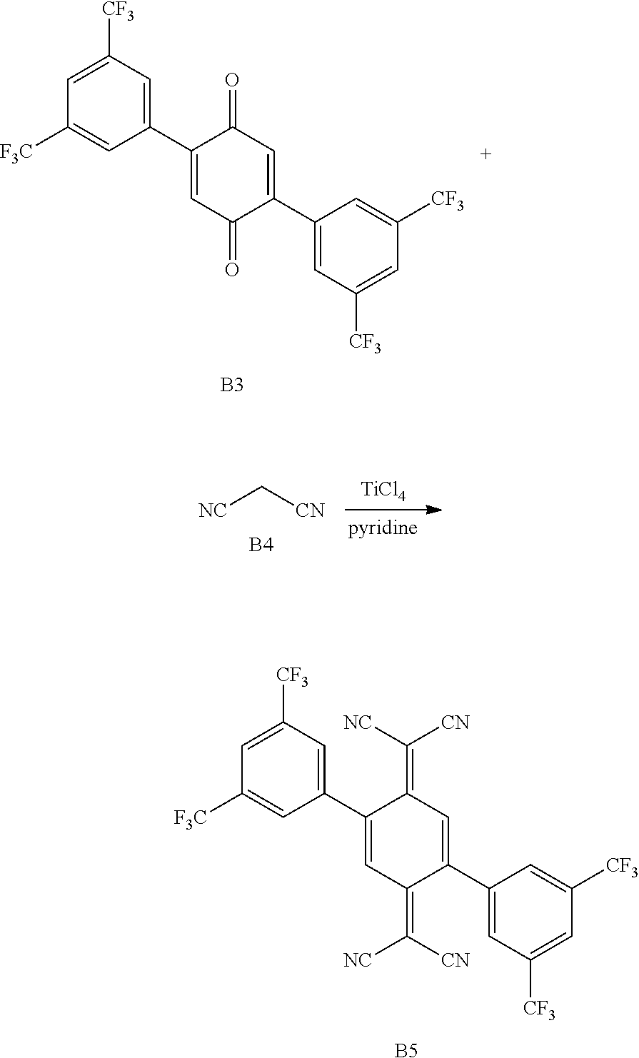
In a 500 ml round-bottom flask, compound B3 (1.65 g, 3.10 mmol) and compound B4 (2.05 g, 31.00 mmol) were added into methylene chloride (250 ml), and the mixture was cooled to 0° C. Then, titanium chloride (3.40 ml, 31.00 mmol) and pyridine (4.99 ml, 62.00 mmol) were slowly and sequentially added dropwise, then stirred at 60° C. for 24 hours. The reaction was terminated, extracted with water and methylene chloride, concentrated, and then subjected to column separation using methylene chloride, ethyl acetate, and n-hexane. Then, a precipitation liquid was formed by using methylene chloride and petroleum ether, then filtered to obtain compound B5 (0.48 g, 0.76 mmol).

In a 500 ml round-bottom flask, compound C1 (4.50 g, 16.92 mmol), compound C2 (6.14 g, 37.23 mmol), tetrakis(triphenylphosphine)palladium(0) (1.96 g, 1.69 mmol), and potassium carbonate (20.58 g, 148.93 mmol) were added into a mixed solution of tetrahydrofurane (180 ml) and water (60 ml), then stirred at 80° C. for 4 hours. The reaction was terminated, extracted with water and ethyl acetate, concentration, and then subjected to column separation using methylene chloride and n-hexane. Then, a precipitation liquid was formed by using methylene chloride and petroleum ether, then filtered to obtain compound C3 (1.35 g, 3.90 mmol).

In a 500 ml round-bottom flask, compound C3 (1.35 g, 3.90 mmol) and compound C4 (2.58 g, 38.98 mmol) were added into methylene chloride (250 ml), and the mixture was cooled to 0° C. Then, titanium chloride (4.27 ml, 38.98 mmol) and pyridine (6.28 ml, 77.97 mmol) were slowly and sequentially added dropwise, then stirred at 60° C. for 24 hours. The reaction was terminated, then extracted with water and methylene chloride, concentrated, and then subjected to column separation using methylene chloride, ethyl acetate, and n-hexane. Then, a precipitation liquid was formed by using methylene chloride and petroleum ether, then filtered to obtain compound C5 (0.52 g, 1.18 mmol).

In a 250 ml round-bottom flask, compound D1 (10.00 g, 51.97 mmol), compound D2 (5.86 g, 51.79 mmol), and potassium carbonate (8.59 g, 62.15 mmol) were added into 100 ml of dimethylformamide, and the mixture was cooled at room temperature for 4 hours. After the reaction was terminated, water and acetic acid were added thereinto, then stirred for 30 minutes, extracted with chloroform, and then concentrated to obtain compound D3 (14.52 g, 97.96 mmol) as a yellow liquid.

Compound D3 (14.52 g, 50.74 mmol) was added in a 100 ml round-bottom flask, and 50% acetic acid (20 ml), and sulfuric acid (1.00 ml) were added thereinto, then stirred at 100° C. for 24 hours. After the reaction was terminated, the reacted material was lowered to room temperature, then extracted with water and chloroform, and then the moisture was removed over magnesium sulfate. The resultant material was dried in a vacuum oven to obtain compound D4 (9.21 g, 43.03 mmol).

In a 500 ml round-bottom flask, compound B3 (2.00 g, 5.78 mmol) and compound B4 (0.57 g, 8.66 mmol) were added into methylene chloride (250 ml), and the mixture was cooled to 0° C. Then, titanium chloride (0.95 ml, 8.66 mmol) and pyridine (1.40 ml, 17.33 mmol) were slowly and sequentially added dropwise, then stirred at room temperature for 24 hours. The reaction was terminated, then extracted with water and methylene chloride, concentrated, and then subjected to column separation using methylene chloride, ethyl acetate, and n-hexane. Then, a precipitation liquid was formed by using methylene chloride and petroleum ether, then filtered to obtain compound A3 (0.82 g, 2.08 mmol).

In a 500 ml round-bottom flask, compound D5 (0.82 g, 2.08 mmol) and compound B4 (4.45 g, 20.79 mmol) were added into methylene chloride (200 ml), and the mixture was cooled to 0° C. Then, titanium chloride (2.28 ml, 20.79 mmol) and pyridine (3.35 ml, 41.59 mmol) were slowly and sequentially added dropwise, then stirred at 60° C. for 24 hours. The reaction was terminated, then extracted with water and methylene chloride, concentrated, and then subjected to column separation using methylene chloride, ethyl acetate, and n-hexane. Then, a precipitation liquid was formed by using methylene chloride and petroleum ether, then filtered to obtain compound D6 (0.48 g, 0.88 mmol).
Hereinafter, organic light emitting devices manufactured by doping charge transporting compounds A, B, A5, B5, C5, and D6 of the present invention, which were prepared in the foregoing synthetic examples, in hole injection layers, respectively.
An ITO substrate was patterned to have a light emission area of 3 mm×3 mm, and then washed. The substrate was mounted on the vacuum chamber and the basic pressure was then set to 1×10⁻⁶ torr. Thereafter, sequentially, a hole injection layer was formed on the ITO as an anode to form a thickness of 100 Å by the use of α-NPD. Compound A was doped at a doping concentration of 25%. A hole transport layer was formed that had a thickness of 600 Å by the use of α-NPD. A light emitting layer was formed that had a thickness of 250 Å by doping a host MADN with a dopant BD-1 at a doping concentration of 4%. An electron transport layer was formed that had a thickness of 300 Å by the use of Alq3. An electron injection layer was formed that had a thickness of 10 Å by the use of LiF. An anode was formed that had a thickness of 300 Å by the use of Alto thereby manufacture an organic light emitting device.

An organic light emitting device was manufactured under the same process conditions as in example 1, except that compound B was doped in a hole injection layer.
An organic light emitting device was manufactured under the same process conditions as in example 1, except that compound A5 was doped in a hole injection layer.
An organic light emitting device was manufactured under the same process conditions as in example 1, except that compound B5 was doped in a hole injection layer.
An organic light emitting device was manufactured under the same process conditions as in example 1, except that compound C5 was doped in a hole injection layer.
An organic light emitting device was manufactured under the same process conditions as in example 1, except that compound D6 was doped in a hole injection layer.
An organic light emitting device was manufactured under the same process conditions as in example 1, except that HAT-CN was doped in a hole injection layer.
An organic light emitting device was manufactured under the same process conditions as in comparative example 1, except that a hole injection layer was formed of DNTPD without doping using any dopant.
An organic light emitting device was manufactured under the same process conditions as in comparative example 2, except that a hole injection layer was not formed.
The driving voltage, quantum efficiency, current efficiency, power efficiency, luminance, and color coordinates of the organic light emitting devices manufactured according to examples 1 and 2 and comparative example 1 were measured, and are shown in table 1 below. In addition, the correlations between voltage and current of the organic light emitting devices, manufactured according to examples 1 and 2 and comparative example 1 of the present invention, are shown in FIG. 7 . (Current corresponds to experimental results values using 10 mA/cm2)
| TABLE 1 | |||
| Emission efficiency | |||
| driving | quantum | current | power |
| voltage | efficiency | efficiency | efficiency | Luminance | color coordinates |
| # | (V) | (%) | (Cd/A) | (lm/W) | (Cd/m2) | CIE_x | CIE_y |
| Comparative | 5.6 | 5.49 | 4.58 | 2.33 | 458 | 0.138 | 0.095 |
| Example | |||||||
| Example 1 | 4.8 | 6.21 | 5.42 | 3.53 | 542 | 0.138 | 0.099 |
| Example 2 | 4.5 | 6.62 | 5.59 | 3.89 | 559 | 0.138 | 0.097 |
Referring to Table 1 and FIG. 7 , an equal level of color coordinates was exhibited between examples 1 and 2 of the present invention and comparative example. Also, the driving voltage was reduced by about 14 to 19% in examples 1 and 2 compared with comparative example 1. In addition, the quantum efficiency, current efficiency, power efficiency, and luminance were further improved in examples 1 and 2 compared with comparative example.
In addition, the driving voltages of the organic light emitting devices manufactured according to examples 3 to 6 and comparative examples 2 and 3 were measured, and are shown in table 2 below. In addition, the correlations between voltage and current of the organic light emitting devices manufactured according to examples 3 to 6 and comparative examples 2 and 3 of the present invention are shown in FIG. 8 .
| TABLE 2 | ||
| Driving voltage (V) | ||
| Example 3 | 4.63 | ||
| Example 4 | 4.51 | ||
| Example 5 | 4.81 | ||
| Example 6 | 4.83 | ||
| Comparative example 2 | 5.27 | ||
| Comparative example 3 | 6.1 | ||
Referring to table 2 and FIG. 8 , the driving voltage was reduced by about 8 to 14% in examples 3 to 6 compared with comparative example 2 and reduced by 21 to 26% compared with comparative example 3.
Although embodiments have been described with reference to a number of illustrative embodiments thereof, it should be understood that numerous other modifications and embodiments can be devised by those skilled in the art that will fall within the scope of the principles of this disclosure. More particularly, various variations and modifications are possible in the component parts and/or arrangements of the subject combination arrangement within the scope of the disclosure, the drawings and the appended claims. In addition to variations and modifications in the component parts and/or arrangements, alternative uses will also be apparent to those skilled in the art.
Claims (38)
1. An organic compound of chemical formula 1:

wherein R1, R2, R3 and R4 each represent, independently of each other, a hydrogen atom, a deuterium atom, —OH, —CN, —NO2, —CF3, a fluoroalkyl group, a halogen group, a carboxyl group, a carbonyl group, a C1-C18 substituted or unsubstituted alkoxy group, a C6 or more substituted or unsubstituted aromatic group, a C5 or more substituted or unsubstituted heteroaromatic group, a C6 or more substituted or unsubstituted aryloxy group, C5 or more substituted or unsubstituted heteroaryloxy group, a C1-C18 amine group, an amine group containing a C6 or more substituted or unsubstituted aromatic group, or an amine group containing a C5 or more substituted or unsubstituted heteroaromatic group;
at least one of R1, R2, R3 and R4 represent a C6 or more substituted or unsubstituted aromatic group, a C5 or more substituted or unsubstituted heteroaromatic group, a C1-C18 amine group, an amine group containing a C6 or more substituted or unsubstituted aromatic group, an amine group containing a C5 or more substituted or unsubstituted heteroaromatic group;
X1 and Y1 each represent, independently from each other, (a), (b), or (d):

and
R5, R6 and R7 each represent, independently from each other, a hydrogen atom, a deuterium atom, —OH, —CN, —NO2, —CF3, a fluoroalkyl group, a halogen group, a carboxyl group, a carbonyl group, a C1-C18 substituted or unsubstituted alkyl group, a C1-C18 substituted or unsubstituted alkoxy group, a C6 or more substituted or unsubstituted aromatic group, a C6 or more substituted or unsubstituted aryloxy group, a C5 or more substituted or unsubstituted heteroaromatic group, or a C5 or more substituted or unsubstituted heteroaryloxy group,
wherein X1 and Y1 are different each other, and
wherein R5 and R6 are optionally linked to each other to form a ring.
2. The organic compound of claim 1 , wherein the compound of chemical formula 1 is selected from:


3. An organic compound of chemical formula 2:

wherein
B1 and B2 each represent, independently from each other, a hydrogen atom, a deuterium atom, —CN, —NO2, —CF3, —F, a fluoroalkyl group, or a halogen group;
R8 to R17 each represent, independently from each other, a hydrogen atom, a deuterium atom, —OH, —CN, —NO2, —CF3, a fluoroalkyl group, a halogen group, a carboxyl group, a carbonyl group, a C1-C18 substituted or unsubstituted alkyl group, a C1-C18 substituted or unsubstituted alkoxy group, a C6 or more substituted or unsubstituted aromatic group, a C5 or more substituted or unsubstituted heteroaromatic group, a C6 or more substituted or unsubstituted aryloxy group, C5 or more substituted or unsubstituted heteroaryloxy group, a C1-C18 amine group, an amine group containing a C6 or more substituted or unsubstituted aromatic group, an amine group containing a C5 or more substituted or unsubstituted heteroaromatic group, a silyl group containing a C1-C27 alkyl group or a C6 or more substituted or unsubstituted aromatic group, or a silyl group containing a C5 or more substituted or unsubstituted heteroaromatic group, and
at least one of R8 to R17 represents —CN, —NO2, —CF3, —F, or a fluoroalkyl group;
X2 and Y2 each represent, independently from each other, (f), or (h):

and
A3 represents a hydrogen atom, a deuterium atom, —OH, —CN, —NO2, —CF3, a fluoroalkyl group, a halogen group, a carboxyl group, a carbonyl group, a C1-C18 substituted or unsubstituted alkyl group, a C1-C18 substituted or unsubstituted alkoxy group, a C6 or more substituted or unsubstituted aromatic group, a C6 or more substituted or unsubstituted aryloxy group, a C5 or more substituted or unsubstituted heteroaromatic group, or a C5 or more substituted or unsubstituted heteroaryloxy group.
4. The organic compound of claim 3 , wherein the organic compound of chemical formula 2 is selected from:
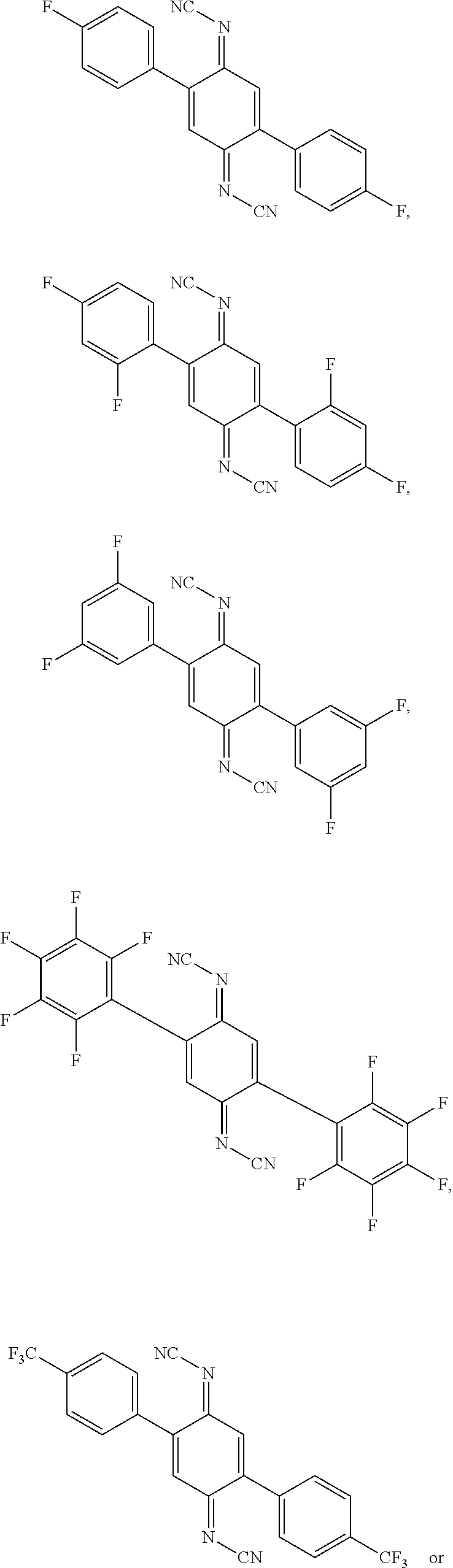

5. An organic light emitting device comprising a light emitting layer between an anode and a cathode, and at least one organic film between the anode and the light emitting layer,
wherein the organic film contains the organic compound of claim 1 .
6. The organic light emitting device of claim 5 , wherein the organic film is at least one selected from a hole injection layer, a hole transport layer, and a hole buffer layer.
7. The organic light emitting device of claim 6 , wherein the hole injection layer is formed of only the organic compound.
8. The organic light emitting device of claim 6 , wherein the hole buffer layer is disposed between the hole injection layer and the hole transport layer, and contacted with the anode.
9. The organic light emitting device of claim 6 , wherein the hole buffer layer is disposed between the hole injection layer and the hole transport layer.
10. The organic light emitting device of claim 8 , wherein the hole buffer layer is formed of only the organic compound, or formed of a host material and the organic compound.
11. The organic light emitting device of claim 10 , wherein the host material is a material of the hole transport layer.
12. The organic light emitting device of claim 6 , wherein the hole transport layer is disposed on the hole injection layer, and formed of a material of the hole transport layer and the organic compound.
13. An organic light emitting device comprising a plurality of stacks between an anode and a cathode, each of the stacks including a light emitting layer, the plurality of stacks including a first stack and a second stack,
wherein the first stack including a first light emitting layer, the second stack includes a second light emitting layer, and a charge generation layer is disposed between the first stack and the second stack,
wherein the charge generation layer includes an N-type charge generation layer and a P-type charge generation layer, and
wherein the P-type charge generation layer contains the organic compound of claim 1 .
14. The organic light emitting device of claim 13 , wherein the first stack includes at least one organic film disposed between the anode and the first light emitting layer, the organic film being at least one of a hole injection layer, a first hole transport layer, and a hole buffer layer.
15. The organic light emitting device of claim 13 , wherein the first stack includes a first hole transport layer, the P-type charge generation layer is formed of only the organic compound or formed of a host material or the organic compound.
16. The organic light emitting device of claim 15 , wherein the host material is a material of the hole transport layer.
17. The organic light emitting device of claim 15 , wherein the second stack includes a second hole transport layer disposed between the P-type charge generation layer and the second light emitting layer.
18. The organic light emitting device of claim 15 , wherein the P-type charge generation layer is contacted with the second light emitting layer.
19. The organic light emitting device of claim 14 , wherein the hole injection layer is formed of only the organic compound.
20. The organic light emitting device of claim 14 , wherein the hole buffer layer is disposed between the anode and the first hole transport layer, and contacted with the anode.
21. The organic light emitting device of claim 14 , wherein the hole buffer layer is disposed between the hole injection layer and the first hole transport layer.
22. The organic light emitting device of claim 20 , wherein the hole buffer layer is formed of only the organic compound, or formed of a host material and the organic compound.
23. The organic light emitting device of claim 22 , wherein the host material is a material of the first hole transport layer.
24. The organic light emitting device of claim 14 , wherein the first hole transport layer is disposed on the hole injection layer, and formed of a material of the first hole transport layer and the organic compound.
25. The organic compound of claim 1 , wherein the organic compound is contained in at least one organic film of an organic light emitting device.
26. The organic compound of claim 1 , wherein the organic compound has electron accepting capacity.
27. The organic compound of claim 25 , wherein the organic film is at least one selected from a hole injection layer, a hole transport layer, and a hole buffer layer.
28. The organic compound of claim 27 , wherein the hole injection layer is formed of only the organic compound.
29. The organic compound of claim 27 , wherein the hole buffer layer is disposed between the hole injection layer and the hole transport layer, and contacted with the anode, the hole buffer layer is disposed between the hole injection layer and the hole transport layer, and the hole buffer layer is formed of only the organic compound, or formed of a host material and the organic compound.
30. The organic compound of claim 27 , wherein the hole transport layer is disposed on the hole injection layer, and formed of a material of the hole transport layer and the organic compound.
31. The organic compound of claim 1 , wherein the compound is contained in an organic light emitting device,
wherein the organic light emitting device comprises comprising a plurality of stacks between an anode and a cathode, each of the stacks including a light emitting layer, the plurality of stacks including a first stack and a second stack,
wherein the first stack includes a first light emitting layer, the second stack includes a second light emitting layer, and a charge generation layer is disposed between the first stack and the second stack,
wherein the charge generation layer includes an N-type charge generation layer and a P-type charge generation layer, and
wherein the compound is contained in the P-type charge generation layer.
32. The organic compound of claim 31 , wherein the first stack includes at least one organic film disposed between the anode and the first light emitting layer, the organic film being at least one of a hole injection layer, a first hole transport layer, and a hole buffer layer.
33. The organic compound of claim 31 , wherein the first stack includes a first hole transport layer, the P-type charge generation layer is formed of only the organic compound or formed of a host material or the organic compound, wherein the host material is a material of the hole transport layer.
34. The organic compound of claim 31 , wherein the second stack includes a second hole transport layer disposed between the P-type charge generation layer and the second light emitting layer, and the P-type charge generation layer is contacted with the second light emitting layer.
35. The organic compound of claim 32 , wherein the hole injection layer is formed of only the organic compound.
36. The organic compound of claim 32 , wherein the hole buffer layer is disposed between the anode and the first hole transport layer, and contacted with the anode, the hole buffer layer is disposed between the hole injection layer and the first hole transport layer, and the hole buffer layer is formed of only the organic compound, or formed of a host material and the organic compound.
37. The organic compound of claim 32 , wherein the first hole transport layer is disposed on the hole injection layer, and formed of a material of the first hole transport layer and the organic compound.
38. An organic compound which is a benzoquinone derivative comprising a substituent having an electron accepting capacity, wherein the organic compound is capable of increasing power efficiency, improving power consumption, and lowering the driving voltage,
wherein the organic compound is selected from:


Applications Claiming Priority (2)
| Application Number | Priority Date | Filing Date | Title |
|---|---|---|---|
| KR10-2013-0149385 | 2013-12-03 | ||
| KR1020130149385A KR102174066B1 (en) | 2013-12-03 | 2013-12-03 | Organic compounds and organic light emitting diode device comprising the same |
Publications (2)
| Publication Number | Publication Date |
|---|---|
| US20150155490A1 US20150155490A1 (en) | 2015-06-04 |
| US10069073B2 true US10069073B2 (en) | 2018-09-04 |
Family
ID=53266047
Family Applications (1)
| Application Number | Title | Priority Date | Filing Date |
|---|---|---|---|
| US14/553,601 Active 2035-02-26 US10069073B2 (en) | 2013-12-03 | 2014-11-25 | Organic compounds and organic light emitting device comprising the same |
Country Status (4)
| Country | Link |
|---|---|
| US (1) | US10069073B2 (en) |
| KR (1) | KR102174066B1 (en) |
| CN (1) | CN104693067B (en) |
| TW (1) | TWI564273B (en) |
Families Citing this family (14)
| Publication number | Priority date | Publication date | Assignee | Title |
|---|---|---|---|---|
| CN105085320B (en) * | 2015-09-08 | 2017-03-22 | 北京大未来生物科技有限公司 | Synthesis method of dicyano substituted biphenyl compounds |
| KR102527772B1 (en) * | 2015-12-30 | 2023-04-28 | 엘지디스플레이 주식회사 | Organic compound and light emitting diode and organic light emitting diode display device using the same |
| KR101973688B1 (en) * | 2016-02-11 | 2019-04-29 | 주식회사 엘지화학 | Compound and organic light emitting device using the same |
| KR102032598B1 (en) * | 2016-06-01 | 2019-10-15 | 주식회사 엘지화학 | Organic light emitting device |
| CN106083652B (en) * | 2016-06-12 | 2017-11-21 | 阜阳欣奕华材料科技有限公司 | A kind of synthetic method of the cyanogen dimethyl-parabenzoquinone of 2,3,5,6 tetrafluoro 7,7 ', 8,8 ' four |
| KR102076882B1 (en) * | 2016-09-29 | 2020-02-12 | 주식회사 엘지화학 | Compound and organic light emitting device using the same |
| KR102073257B1 (en) * | 2016-11-08 | 2020-02-04 | 주식회사 엘지화학 | Organic light emitting device |
| KR102109075B1 (en) * | 2017-02-24 | 2020-05-11 | 주식회사 엘지화학 | Organic light emitting device |
| KR102098221B1 (en) * | 2017-02-24 | 2020-04-07 | 주식회사 엘지화학 | Organic light emitting device |
| US11466009B2 (en) | 2017-12-13 | 2022-10-11 | Beijing Summer Sprout Technology Co., Ltd. | Organic electroluminescent materials and devices |
| CN114920757A (en) | 2017-12-13 | 2022-08-19 | 北京夏禾科技有限公司 | Organic electroluminescent materials and devices |
| US11897896B2 (en) | 2017-12-13 | 2024-02-13 | Beijing Summer Sprout Technology Co., Ltd. | Organic electroluminescent materials and devices |
| US11466026B2 (en) | 2017-12-13 | 2022-10-11 | Beijing Summer Sprout Technology Co., Ltd. | Organic electroluminescent materials and devices |
| CN110372540B (en) * | 2018-04-12 | 2022-11-11 | 武汉尚赛光电科技有限公司 | 3, 6-di (prop-2-ylidene) cyclohexa-1, 4-diene derivatives, methods of making, uses, and devices |
Citations (5)
| Publication number | Priority date | Publication date | Assignee | Title |
|---|---|---|---|---|
| JPS63203656A (en) | 1987-02-19 | 1988-08-23 | Osaka Yuki Kagaku Kogyo Kk | Tetracyanoquinodimethane having phenyl group or phenyl-substituted group |
| CN101410364A (en) | 2006-03-30 | 2009-04-15 | 出光兴产株式会社 | Material for organic electroluminescent element and organic electroluminescent element using same |
| JP2010044882A (en) | 2008-08-08 | 2010-02-25 | Osaka City Univ | Electrode active material, and secondary battery |
| JP2011086442A (en) | 2009-10-14 | 2011-04-28 | Konica Minolta Holdings Inc | Organic electroluminescent element and lighting system |
| US20120193619A1 (en) | 2009-10-14 | 2012-08-02 | Konica Minolta Holdings, Inc. | Organic electroluminescent element and lighting device using same |
Family Cites Families (5)
| Publication number | Priority date | Publication date | Assignee | Title |
|---|---|---|---|---|
| JPH08305052A (en) * | 1995-05-10 | 1996-11-22 | Konica Corp | Electrophotographic photoreceptor, electrophotographic device and device unit |
| US7629741B2 (en) * | 2005-05-06 | 2009-12-08 | Eastman Kodak Company | OLED electron-injecting layer |
| KR100839750B1 (en) * | 2007-01-15 | 2008-06-19 | 삼성에스디아이 주식회사 | Organic light emitting display |
| US20100294368A1 (en) * | 2009-05-22 | 2010-11-25 | Konica Minolta Business Technologies, Inc. | Photoelectric conversion element and solar cell |
| KR101365824B1 (en) * | 2010-10-22 | 2014-02-20 | 엘지디스플레이 주식회사 | Organic Light Emitting Diode Device |
-
2013
- 2013-12-03 KR KR1020130149385A patent/KR102174066B1/en active IP Right Grant
-
2014
- 2014-11-25 US US14/553,601 patent/US10069073B2/en active Active
- 2014-11-26 TW TW103141062A patent/TWI564273B/en active
- 2014-12-02 CN CN201410721124.9A patent/CN104693067B/en active Active
Patent Citations (5)
| Publication number | Priority date | Publication date | Assignee | Title |
|---|---|---|---|---|
| JPS63203656A (en) | 1987-02-19 | 1988-08-23 | Osaka Yuki Kagaku Kogyo Kk | Tetracyanoquinodimethane having phenyl group or phenyl-substituted group |
| CN101410364A (en) | 2006-03-30 | 2009-04-15 | 出光兴产株式会社 | Material for organic electroluminescent element and organic electroluminescent element using same |
| JP2010044882A (en) | 2008-08-08 | 2010-02-25 | Osaka City Univ | Electrode active material, and secondary battery |
| JP2011086442A (en) | 2009-10-14 | 2011-04-28 | Konica Minolta Holdings Inc | Organic electroluminescent element and lighting system |
| US20120193619A1 (en) | 2009-10-14 | 2012-08-02 | Konica Minolta Holdings, Inc. | Organic electroluminescent element and lighting device using same |
Non-Patent Citations (9)
| Title |
|---|
| Asakawa et al., J. Phys. Chem., 8, 2012, 116, pp. 4016-4023. * |
| Aumuller, et al. "N,N-Dicy noquinonediimines-A New Class of Compounds, II: Comparison of Redox Properties with those of Quinones and Tetracyanoquinodimethanes", Leibigs Ann. Chem 1986, p. 165-176. |
| Aumuller, et al. "N,N—Dicy noquinonediimines—A New Class of Compounds, II: Comparison of Redox Properties with those of Quinones and Tetracyanoquinodimethanes", Leibigs Ann. Chem 1986, p. 165-176. |
| Cosimbescu et al., "7,7,8,8-Tetracyanoquinodimethane-Based Molecular Dopants for p-Type Doping of OLEOs: A Theoretical Investigation", J. Phys. Chem. A 2011, vol. 115, p. 13498-13503. |
| Registry, RN: 1284234-08-7 (STN search data-annex 1), Apr. 22, 2011. |
| Registry, RN: 60421-85-4 (STN search data-annex 2), Nov. 16, 1584. |
| STN database entry for CAS RN 851-40-1. Entered STN Nov. 16, 1984. Accessed Aug. 8, 2017. * |
| STN Registry Database entry for CAS RN 1071142-96-5, Entry date Nov. 6, 2008; Accessed Oct. 2, 2016. * |
| STN Registry Database entry for CAS RN 1332075-10-1, Entry date Sep. 13, 2011; Accessed Apr. 5, 2017. * |
Also Published As
| Publication number | Publication date |
|---|---|
| TWI564273B (en) | 2017-01-01 |
| CN104693067B (en) | 2018-05-29 |
| US20150155490A1 (en) | 2015-06-04 |
| CN104693067A (en) | 2015-06-10 |
| KR102174066B1 (en) | 2020-11-05 |
| KR20150064795A (en) | 2015-06-12 |
| TW201529533A (en) | 2015-08-01 |
Similar Documents
| Publication | Publication Date | Title |
|---|---|---|
| US10069073B2 (en) | Organic compounds and organic light emitting device comprising the same | |
| US9793489B2 (en) | Pyrene compound and organic light emitting diode device including the same | |
| US9281487B2 (en) | White organic light emitting diode device | |
| KR102268119B1 (en) | Pyrene compound and organic light emitting diode device comprising the same | |
| KR102525492B1 (en) | Organic light emitting device | |
| US20110121268A1 (en) | Light-emitting element | |
| US20230389415A1 (en) | Organic Light Emitting Display Device | |
| US9865822B2 (en) | Blue phosphorescence compound and organic light emitting diode using the same | |
| US10355220B2 (en) | Organic light emitting display device | |
| US20140061601A1 (en) | Anthracene compound and organic light emitting diode including the same | |
| US8632893B2 (en) | Organic compound and organic electroluminescence device employing the same | |
| US9130173B2 (en) | Quinolino[3,2,1-kl]phenoxazine compound and organic light emitting element using the same | |
| CN111785841B (en) | Organic electroluminescent device and application thereof | |
| KR102169515B1 (en) | Quinone derivatives and organic light emitting diode device comprising the same | |
| KR102152013B1 (en) | Organic light emitting diode device comprising organic compounds | |
| US9178164B2 (en) | Organic compound and organic electroluminescent device employing the same | |
| KR102242870B1 (en) | Heterocyclic compounds and organic light emitting diode device comprising the same | |
| KR102181332B1 (en) | Heterocyclic compounds and organic light emitting diode device comprising the same | |
| KR102181311B1 (en) | Organic compounds and organic light emitting diode device comprising the same | |
| KR102175791B1 (en) | Organic compounds and organic light emitting diode device comprising the same | |
| KR102145425B1 (en) | Organic compounds and organic light emitting diode device comprising the same | |
| KR102228323B1 (en) | Compound and organic light emitting device comprising the same | |
| US20210024496A1 (en) | Organic compound, organic light emitting diode and organic light emitting display device including the compound | |
| WO2014007022A1 (en) | Light emitting element material and light emitting element | |
| KR20150065393A (en) | Organic light emitting diode devices |
Legal Events
| Date | Code | Title | Description |
|---|---|---|---|
| AS | Assignment |
Owner name: LG DISPLAY CO., LTD., KOREA, REPUBLIC OF Free format text: ASSIGNMENT OF ASSIGNORS INTEREST;ASSIGNORS:RYU, YOUNGJU;LEE, SEUNGJAE;BIN, JONGKWAN;AND OTHERS;REEL/FRAME:034273/0133 Effective date: 20141118 |
|
| STCF | Information on status: patent grant |
Free format text: PATENTED CASE |
|
| MAFP | Maintenance fee payment |
Free format text: PAYMENT OF MAINTENANCE FEE, 4TH YEAR, LARGE ENTITY (ORIGINAL EVENT CODE: M1551); ENTITY STATUS OF PATENT OWNER: LARGE ENTITY Year of fee payment: 4 |