US8294175B2 - Light-emitting device and display - Google Patents
Light-emitting device and display Download PDFInfo
- Publication number
- US8294175B2 US8294175B2 US12/985,079 US98507911A US8294175B2 US 8294175 B2 US8294175 B2 US 8294175B2 US 98507911 A US98507911 A US 98507911A US 8294175 B2 US8294175 B2 US 8294175B2
- Authority
- US
- United States
- Prior art keywords
- layer
- light
- opening
- electrode
- conductive
- Prior art date
- Legal status (The legal status is an assumption and is not a legal conclusion. Google has not performed a legal analysis and makes no representation as to the accuracy of the status listed.)
- Expired - Fee Related, expires
Links
Images


Classifications
-
- H—ELECTRICITY
- H10—SEMICONDUCTOR DEVICES; ELECTRIC SOLID-STATE DEVICES NOT OTHERWISE PROVIDED FOR
- H10H—INORGANIC LIGHT-EMITTING SEMICONDUCTOR DEVICES HAVING POTENTIAL BARRIERS
- H10H20/00—Individual inorganic light-emitting semiconductor devices having potential barriers, e.g. light-emitting diodes [LED]
- H10H20/80—Constructional details
- H10H20/81—Bodies
- H10H20/819—Bodies characterised by their shape, e.g. curved or truncated substrates
-
- H—ELECTRICITY
- H10—SEMICONDUCTOR DEVICES; ELECTRIC SOLID-STATE DEVICES NOT OTHERWISE PROVIDED FOR
- H10H—INORGANIC LIGHT-EMITTING SEMICONDUCTOR DEVICES HAVING POTENTIAL BARRIERS
- H10H20/00—Individual inorganic light-emitting semiconductor devices having potential barriers, e.g. light-emitting diodes [LED]
- H10H20/80—Constructional details
- H10H20/85—Packages
- H10H20/852—Encapsulations
- H10H20/853—Encapsulations characterised by their shape
-
- H—ELECTRICITY
- H10—SEMICONDUCTOR DEVICES; ELECTRIC SOLID-STATE DEVICES NOT OTHERWISE PROVIDED FOR
- H10H—INORGANIC LIGHT-EMITTING SEMICONDUCTOR DEVICES HAVING POTENTIAL BARRIERS
- H10H20/00—Individual inorganic light-emitting semiconductor devices having potential barriers, e.g. light-emitting diodes [LED]
- H10H20/01—Manufacture or treatment
- H10H20/011—Manufacture or treatment of bodies, e.g. forming semiconductor layers
- H10H20/018—Bonding of wafers
Definitions
- the present disclosure relates to a light-emitting device that does not include an electrode on a light emission surface and a display including the light-emitting device in each pixel.
- LEDs Light Emitting Diodes
- LEDs Light Emitting Diodes
- backlights of liquid crystal displays display panels of LED displays and lighting fixtures. Accordingly, cost reduction in LEDs is strongly desired.
- cost reduction in LEDs is strongly desired.
- an improvement in productivity, selection of low-cost materials and the like are necessary.
- a chip size is reduced to produce a large number of LEDs from one wafer.
- the chip size is extremely small, for example, 20 ⁇ m, and it is difficult to handle a single LED chip. Therefore, it is not realistic to mount each LED chip on a circuit board with use of a mounter.
- a supporting wafer including an adhesive layer on a surface thereof is prepared.
- the surface where the adhesive layer is provided of the supporting wafer is brought into contact with a surface on an LED side of a wafer formed by forming a plurality of LEDs in a matrix on a substrate, and then LEDs are separated from the wafer at predetermined intervals by laser lift-off to transfer the LEDs to the supporting wafer. Accordingly, the arrangement pitch of the LEDs is sparse.
- a circuit board (a glass substrate) in which connection electrodes are formed with a pitch equal to the sparse arrangement pitch of the LEDs is prepared, and the LEDs adhered to the supporting wafer are transferred to the circuit board.
- a mounting board formed by mounting the LEDs on the circuit board is allowed to be formed.
- a light-emitting device including: a semiconductor layer including a first conductive contact layer, a first conductive cladding layer, an active layer, a second conductive cladding layer, a second conductive contact layer and a resin block layer in this order.
- the light-emitting device further includes a first electrode in contact with the first conductive contact layer; and a second electrode in contact with the second conductive contact layer.
- the second conductive contact layer includes a first opening at least in a region facing the first electrode.
- the resin block layer includes a plurality of second openings communicated with the first opening, and the first opening has an air gap.
- the first opening is arranged at least in a region facing the first electrode, and the resin block layer including a plurality of second openings communicated with the first opening is arranged outside the second conductive layer. Therefore, when the light-emitting device according to the embodiment is fixed to a supporting substrate with, for example, a resin layer in between, the resin block layer is allowed to prevent the resin layer from being injected into the first opening so that an air gap in the first opening is completely filled with the resin layer.
- a display including: a display panel including a plurality of light-emitting devices which are fixed to a supporting substrate with a resin layer in between, and a drive section driving each of the light-emitting devices.
- Each of the light-emitting devices mounted in the display includes: a semiconductor layer including a first conductive contact layer, a first conductive cladding layer, an active layer, a second conductive cladding layer, a second conductive contact layer and a resin block layer in order of decreasing distance from the supporting substrate.
- Each of the light-emitting device further includes a first electrode in contact with the first conductive contact layer; and a second electrode in contact with the second conductive contact layer.
- the second conductive contact layer includes a first opening at least in a region facing the first electrode.
- the resin block layer includes a plurality of second openings communicated with the first opening, and the first opening has an air gap.
- the first opening is arranged at least in a region facing the first electrode, and the resin block layer including a plurality of second openings communicated with the first opening is arranged outside the second conductive layer. Therefore, when the display according to the embodiment is manufactured, for example, by fixing the light-emitting devices to the supporting substrate with the resin layer in between, the resin block layer is allowed to prevent the resin layer from being injected into the first opening so that an air gap in the first opening is completely filled with the resin layer, and as a result, in the display according to the embodiment, an air gap remains in the first opening.
- the light-emitting device when the light-emitting device is fixed to the supporting substrate with the resin layer in between, an air gap is formed in the first opening of the second conductive contact layer in contact with the second electrode. Therefore, a whole light emission surface of the light-emitting device is not adhered to the resin layer, so a decline in light extraction efficiency is preventable.
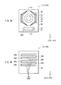
- FIG. 1 is a perspective view of a display according to an embodiment.
- FIG. 2 is a top view of an image display region in FIG. 1 .
- FIGS. 3A and 3B are a top view and a bottom view of a light-emitting device in FIG. 1 .
- FIG. 4 is a sectional view taken along an arrow direction A-A of the light-emitting device in FIGS. 3A and 3B .
- FIG. 5 is a top view illustrating crystal planes of a mesa section in FIGS. 3A and 3B .
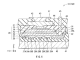
- FIG. 6 is a sectional view of the light-emitting device in the display in FIG. 1 .
- FIGS. 7A and 7B are sectional views for describing an example of a method of manufacturing the light-emitting device in FIG. 4 .
- FIGS. 8A and 8B are sectional views for describing an example of steps following FIGS. 7A and 7B .
- FIGS. 9A and 9B are sectional views for describing an example of steps following FIGS. 8A and 8B .
- FIGS. 10A and 10B are sectional views for describing an example of steps following FIGS. 9A and 9B .
- FIG. 1 illustrates a perspective view of an example of a schematic configuration of a display 1 according to an embodiment.
- the display 1 according to the embodiment is a so-called LED display, and uses LEDs as display pixels.
- the display 1 includes a display panel 10 (a supporting substrate) and a drive IC 20 (a drive section).
- the display panel 10 includes an image display region 10 A and a ring-shaped frame region 10 B around the image display region 10 A in one surface thereof.
- a plurality of data lines 11 are formed so as to extend in a vertical direction (in a vertical direction in the drawing) and to be arranged in parallel with a predetermined pitch.
- a plurality of scan lines 12 are formed so as to extend in a direction intersecting the data lines 11 , more specifically in a horizontal direction (a horizontal direction in the drawing) and to be arranged in parallel with a predetermined pitch.
- the data lines 11 and the scan lines 12 intersect each other (orthogonally intersect each other in FIG. 2 ) in the image display region 10 A when viewed from the direction of the normal to the display panel 10 .
- the scan lines 12 are formed in, for example, an outermost layer, and the data lines 11 are formed in a different layer (a layer below the outermost layer) from the outermost layer including the scan lines 12 .
- Display pixels 13 are arranged in intersections of the data lines 11 and the scan lines 12 , and a plurality of display pixels 13 are arranged in a grid pattern in the image display region 10 A.
- FIG. 2 illustrates the case where three light-emitting devices 14 configure one display pixel 13 and one display pixel 13 is allowed to emit light beams of three primary colors RGB.
- the light-emitting devices 14 are, for example, LEDs.
- a pair of electrodes 21 and 22 for injecting a current to the light-emitting device 14 are arranged on a top surface 14 A of the light-emitting device 14 .
- the electrode 21 of the two electrodes 21 and 22 arranged on the top surface 14 A is electrically connected to the data line 11 through, for example, a bonding wire.
- the electrode 22 of the two electrodes 21 and 22 arranged on the top surface 14 A is electrically connected to the scan line 12 through, for example, a bonding wire.
- the light-emitting device 14 further includes a semiconductor layer 29 including a p-type contact layer 23 , a p-type cladding layer 24 , an active layer 25 , an n-type cladding layer 26 , an n-type contact layer 27 and a resin block layer 28 in this order from a side close to the electrode 21 .
- the p-type contact layer 23 is made of, for example, p-type GaAs
- the p-type cladding layer 24 is made of, for example, p-type AlGaInP.
- the active layer 25 has, for example, a quantum well structure configured by alternately laminating a well layer made of GaInP and a barrier layer made of AlGaInP. If necessary, the active layer 25 may include a pair of guide layers between which the quantum well structure is sandwiched.
- the guide layers are made of, for example, AlGaInP.
- the n-type cladding layer 26 is made of, for example, n-type AlGaInP
- the n-type contact layer 27 is made of, for example, n-type GaAs.
- the resin block layer 28 is made of a material allowed to be subjected to selective wet etching in relation to GaAs, for example, n-type AlGaInP.
- the p-type cladding layer 24 and the n-type cladding layer 26 have a lower refractive index and a larger band gap than those of the active layer 25 .
- the semiconductor layer 29 has a double heterostructure, and functions as a light-emitting diode (LED) emitting light of a wavelength corresponding to the band gap of the active layer 25 from the active layer 25 by current injection.
- LED light-emitting diode
- the electrode 21 is formed, for example, by laminating palladium (Pd), platinum (Pt) and gold (Au) in this order on the p-type contact layer 23 .
- the electrode 22 is formed, for example, by laminating an alloy of gold (Au) and germanium (Ge), nickel (Ni) and gold (Au) in this order.
- the mesa section 30 has the shape of a truncated octagonal pyramid.
- the mesa section 30 is an octagonal prism with a top surface and a bottom surface in which the top surface and the bottom surface are parallel to each other and the top surface is smaller than the bottom surface.
- the top surface of the mesa section 30 is a (001) plane.
- the bottom surface of the mesa section 30 is a (00-1) plane.
- a pair of side surfaces extending in a longitudinal direction of the mesa section 30 in eight side surfaces of the mesa section 30 are a (111) plane and a ( ⁇ 1-11) plane.
- a pair of side surfaces extending in a lateral direction of the mesa section 30 in the eight side surfaces of the mesa section 30 are a (1-10) plane and a ( ⁇ 110) plane.
- the remaining four side surfaces in the eight side surfaces of the mesa section 30 are (1-22) plane, a (2-12) plane, a ( ⁇ 122) plane and a (1-22) plane.
- the n-type cladding layer 26 is exposed on a base of the mesa section 30 .
- An opening 26 A is formed in a part exposed to the base of the mesa section 14 of the n-type cladding layer 26 .
- a top surface of the n-type contact layer 27 is exposed to a bottom surface of the opening 26 A.
- the electrode 22 is in contact with the surface exposed to the bottom surface of the opening 26 A of the n-type contact layer 27 , and the n-type contact layer 27 and the electrode 22 are electrically connected to each other.
- the electrode 21 is in contact with a top surface of the p-type contact layer 23 , and the p-type contact layer 23 and the electrode 21 are electrically connected to each other.
- an opening 27 A (a first opening) is arranged in the n-type contact layer 27 .
- the opening 27 A is arranged at least in a region facing the electrode 21 .
- the opening 27 A is an air gap, and a bottom surface 26 B (a surface on a side close to the n-type contact layer 27 ) of the n-type cladding layer 26 configures a light emission surface.
- each of the openings 28 A is communicated with the opening 27 A, and is an air gap.
- each of the openings 28 A extends in a direction (a first direction) perpendicular to a (110) plane, and has a rectangular shape.
- a part between adjacent openings 28 A of the resin block layer 28 is a rod-shaped beam section 28 B extending in the direction perpendicular to the (110) plane.
- each beam section 28 B has inclined surfaces 28 C and 28 D formed of a (111) plane and a ( ⁇ 1-11) plane as side surfaces.
- each opening 28 A that is, the thickness of the resin block layer 28 is larger than the thickness of the n-type contact layer 27 (for example, tens of nm). Moreover, the width of each opening 28 A (the width of a narrowest part) is equal to or smaller than the width of each beam section 28 B (the width of a widest part).
- FIG. 6 illustrates an example of a sectional configuration of a part including the light-emitting device 14 when the light-emitting device 14 is mounted in the image display region 10 A of the display panel 10 .
- the light-emitting device 14 is fixed on a supporting substrate 40 with a resin layer 41 in between.
- the resin block layer 28 which is a layer closest to the supporting substrate 40 in the semiconductor layer 29 is in contact with the resin layer 41 , and each of the openings 28 A arranged in the resin block layer 28 is filled with the resin layer 41 .
- the resin layer 41 is slightly charged into the opening 27 A arranged in the n-type contact layer 27 ; therefore, the opening 27 A has an air gap.
- a surface exposed to the inside of the opening 27 A of the n-type cladding layer 26 is in contact with air with a refractive index of 1, and is not in contact with the resin layer 41 .
- the electrode 21 of the light-emitting device 14 is electrically connected to an extraction electrode 43 exposed on a top surface of the image display region 10 A through a bump 42 arranged in the image display region 10 A.
- the electrode 22 of the light-emitting device 14 is electrically connected to an extraction electrode 45 exposed on the top surface of the image display region 10 A through a bump 44 arranged in the image display region 10 A.
- the light-emitting device 14 , the bumps 42 and 44 and parts of the extraction electrodes 43 and 45 are covered with the resin layers 46 and 47 .
- the bumps 42 and 44 and the extraction electrodes 43 and 45 are made of, for example, metal including Au, Al, Cr, Ti, Ag or Cu as a main component.
- the resin layer 46 is made of, for example, an epoxy adhesive, and the resin layer 47 is made of, for example, a CRC polyimide-based material.
- FIGS. 7A and 7B to 10 A and 10 B are sectional views illustrating an example of steps of manufacturing the light-emitting device 14 in order.
- a substrate 31 which is a growth substrate for forming the semiconductor layer 29 by crystal growth is prepared, and then, for example, the resin block layer 28 , the n-type contact layer 27 , the n-type cladding layer 26 , the active layer 25 , the p-type cladding layer 24 and the p-type contact layer 23 are formed in this order on the substrate 31 (refer to FIG. 7A ).
- a mask with a predetermined shape (not illustrated) is formed on the p-type contact layer 23 , and then the p-type contact layer 23 is selectively removed with use of a phosphoric acid mixture (phosphoric acid 6:hydrogen peroxide water 2:water 100). After that, the mask is removed.
- a phosphoric acid mixture phosphoric acid 6:hydrogen peroxide water 2:water 100
- a rectangular mask (not illustrated) is formed on a surface of the p-type cladding layer 24 including the p-type contact layer 23 so that the longitudinal direction of the mask is perpendicular to a [110] direction, and then parts of the p-type cladding layer 24 , the active layer 25 , the n-type cladding layer 26 and the n-type contact layer 27 are selectively removed with use of an etching solution formed by cooling hydrochloric acid to ⁇ 15° C. Thus, the mesa section 30 is formed (refer to FIG. 7B ). Such an etching process may be completed by performing etching a plurality of times.
- the rate of etching the (111) plane and the ( ⁇ 1-11) plane is approximately one hundredth of the rate of etching the (1-10) plane and the ( ⁇ 110) plane. Therefore, in the above-described etching process, the (111) plane and the ( ⁇ 1-11) plane are exposed on a long side of the mask extending in a direction perpendicular to a [110] direction to reduce the etching rate. Therefore, when the above-described etching process is completed, a pair of side surfaces extending in the longitudinal direction of the mesa section 30 form the (111) plane and the ( ⁇ 1-11) plane.
- the (111) plane and the ( ⁇ 1-11) plane are not exposed as etching planes on a short side of the mask extending in a direction parallel to the [110] direction. Therefore, the reaction of etching on the (110) plane proceeds, and etching proceeds to a short side region of the mask without reducing the etching rate to form the (1-10) plane and the ( ⁇ 110) plane (a vertical plane). At this time, side etching occurs at corners of the mask to form the (1-22) plane, the (2-12) plane, the ( ⁇ 122) plane and the (1-22) plane. Thus, the mesa section 30 having crystal planes illustrated in FIG. 5 is formed.
- the mask is removed, and then the opening 26 A is formed in a part of the base of the mesa section 30 of the n-type cladding layer 26 to expose the n-type contact layer 27 on the bottom surface of the opening 26 A (refer to FIG. 7B ).
- the electrode 21 is formed on the top surface of the p-type contact layer 23 by, for example, evaporation, and the electrode 22 is formed on a surface of the n-type contact layer 27 exposed on the bottom surface of the opening 26 A by, for example, evaporation (refer to FIG. 8A ).
- a wafer 100 is formed.
- a light coating of a CRC polyimide-based material allowed to be separated by laser ablation is applied to the supporting substrate 32 and is cured to form a wafer 200 having a release layer 33 on the supporting substrate 32 .
- the wafer 200 is bonded to a surface including the mesa section 30 of the wafer 100 with an epoxy-based adhesive 34 in between so that the release layer 33 faces the mesa section 30 (refer to FIG. 8B ).
- the wafer 100 and wafer 200 are bonded together in a low vacuum so as to prevent the entry of air bubbles into the adhesive 34 , and the adhesive 34 is thermally cured while the adhesive 34 is subjected to weight bearing.
- the substrate 31 is removed. More specifically, the substrate 31 is lapped until a predetermined thickness, and then the remaining substrate 31 is completely removed with a solution including an ammonia-hydrogen peroxide water to expose the resin block layer 28 .
- a resist mask 35 having a plurality of striped openings 35 A is formed on a surface of the exposed resin block layer 28 (refer to FIG. 9A ). Each of the openings 35 A is arranged corresponding to a part where the beam section 28 is formed, and extends in a direction perpendicular to the [110] direction.
- the resin block layer 28 is selectively removed with use of, for example, an etching solution formed by cooling hydrochloric acid to ⁇ 15° C. Therefore, the openings 28 A and the beam sections 28 B are formed in the resin block layer 28 , and the n-type contact layer 27 is exposed on the bottom surfaces of the openings 28 A.
- the rate of etching the (111) plane and the ( ⁇ 1-11) plane is approximately one hundredth of the rate of etching the (1-10) plane and the ( ⁇ 110) plane. Therefore, in the above-described etching process, the (111) plane and the ( ⁇ 1-11) plane are exposed on the long sides of opening 35 A extending in a direction perpendicular to the [110] direction to reduce the etching rate. Therefore, when the above-described etching process is completed, a pair of side surfaces 28 C and 28 D extending in the longitudinal direction of the beam section 28 B form the (111) plane and the ( ⁇ 1-11) plane.
- the (111) plane and the ( ⁇ 1-11) plane are not exposed as etching planes on the short sides of the opening 35 A. Therefore, the reaction of etching on the (110) plane proceeds, and etching proceeds to a short side region of the opening 35 A without reducing the etching rate to form the (1-10) plane and the ( ⁇ 110) plane (the vertical plane).
- the beam section 28 B having the (111) plane and the ( ⁇ 1-11) plane as the side surfaces 28 C and 28 D is formed.
- a surface of the n-type contact layer 27 exposed on the bottom surfaces of the openings 28 A is immersed in a phosphoric acid solution for a predetermined time to selectively remove not only parts corresponding to the bottom surfaces of the openings 28 A of the n-type contact layer 27 but also parts corresponding to the beam sections 28 B of the n-type contact layer 27 . Therefore, the opening 27 A communicated with each of the openings 28 A is formed at least in a region facing the electrode 21 of the n-type contact layer 27 (refer to FIG. 10A ). At this time, both of the opening 27 A and each of the openings 28 A are air gaps, and the beam sections 28 B are located in midair. Thus, a plurality of light-emitting devices 14 are formed on the wafer 200 .
- the resist mask 35 is removed, and then the resin block layer 28 , the n-type contact layer 27 and the adhesive 34 are selectively removed by, for example, RIE (Reactive Ion Etching) to expose the release layer 33 (refer to FIG. 10B ). Therefore, the light-emitting devices 14 formed on the wafer 200 are separated from one another to form chips. Thus, the light-emitting device 14 according to the embodiment is formed.
- RIE Reactive Ion Etching
- the respective light-emitting devices 14 on the wafer 200 are adhered to the resin layer 41 applied to the supporting substrate 40 , and laser light is applied to the release layer 33 to ablate the release layer 33 .
- the respective light-emitting devices 14 are allowed to be transferred to the supporting substrate 40 . In doing so, each of the light-emitting devices 14 is allowed to be mounted on the display pixel 13 .
- the opening 27 A is arranged at least in the region facing the electrode 21 , and the resin block layer 28 including a plurality of openings 28 A communicated with the opening 27 A is arranged outside the n-type contact layer 27 (on a light emission side).
- the depth of each opening 28 A that is, the thickness of the resin block layer 28 is larger than the thickness of the n-type contact layer 27 (for example, by tens of nm).
- the resin block layer 28 is allowed to effectively prevent the resin layer 41 from being injected into the opening 27 A so that an air gap in the opening 27 A is completely filled with the resin layer 41 .
- an air gap remains in the opening 27 A in the display 1 . Therefore, in the embodiment, whole light emission surfaces (the bottom surface 26 B of the n-type cladding layer 26 ) of the light-emitting devices 14 are not adhered to the resin layer 41 , so a decline in light extraction efficiency is allowed to be prevented.
- the thickness of the n-type contact layer 27 is extremely thin, for example, approximately tens of nm, and the volume of air contained in the opening 27 A formed in the n-type contact layer 27 is extremely small. Therefore, for example, in the process of manufacturing the display 1 , in the case where the light-emitting devices 14 are transferred to the supporting substrate 40 and then heat is applied to air in the opening 27 A, the possibility that the light-emitting devices 14 are separated from the substrate 40 by expansion of air is allowed to be eliminated.
- the above-described embodiment is applied to wires (data lines 11 ) extending in the vertical direction and a drive IC driving the wires is described. However, the embodiment is applicable to wires (scan lines 12 ) extending in a horizontal direction and a drive IC driving the wires.
- the above-described embodiment is applied to an LED display.
- the embodiments are applicable to any other displays.
- the above-described embodiment is applied to a simple matrix drive display, but the embodiment is applicable to an active matrix drive display.
Landscapes
- Led Devices (AREA)
- Led Device Packages (AREA)
- Devices For Indicating Variable Information By Combining Individual Elements (AREA)
Abstract
Description
-
- 1. Configurations of display and light-emitting device
- 2. Method of manufacturing light-emitting device
- 3. Effects of display
Claims (6)
Applications Claiming Priority (2)
| Application Number | Priority Date | Filing Date | Title |
|---|---|---|---|
| JPP2010-007362 | 2010-01-15 | ||
| JP2010007362A JP2011146597A (en) | 2010-01-15 | 2010-01-15 | Light-emitting device, and display |
Publications (2)
| Publication Number | Publication Date |
|---|---|
| US20110175860A1 US20110175860A1 (en) | 2011-07-21 |
| US8294175B2 true US8294175B2 (en) | 2012-10-23 |
Family
ID=44277279
Family Applications (1)
| Application Number | Title | Priority Date | Filing Date |
|---|---|---|---|
| US12/985,079 Expired - Fee Related US8294175B2 (en) | 2010-01-15 | 2011-01-05 | Light-emitting device and display |
Country Status (2)
| Country | Link |
|---|---|
| US (1) | US8294175B2 (en) |
| JP (1) | JP2011146597A (en) |
Families Citing this family (6)
| Publication number | Priority date | Publication date | Assignee | Title |
|---|---|---|---|---|
| FR2998096B1 (en) * | 2012-11-14 | 2015-01-30 | Astron Fiamm Safety | ELECTRICAL CONNECTION OF AN OLED DEVICE |
| KR20150025231A (en) * | 2013-08-28 | 2015-03-10 | 서울반도체 주식회사 | Light source module and manufacturing method thereof, backlight unit |
| US9385279B2 (en) * | 2014-05-30 | 2016-07-05 | Nichia Corporation | Light-emitting device and method for manufacturing the same |
| TWM521008U (en) * | 2016-01-27 | 2016-05-01 | Lite On Technology Corp | Lamp device and its lighting module |
| WO2021070977A1 (en) * | 2019-10-07 | 2021-04-15 | 엘지전자 주식회사 | Display device using micro led and method of manufacturing same |
| CN111864019B (en) * | 2020-07-10 | 2021-11-30 | 武汉大学 | Flip light-emitting diode with embedded scattering layer and preparation method thereof |
Citations (3)
| Publication number | Priority date | Publication date | Assignee | Title |
|---|---|---|---|---|
| JP2002118124A (en) | 2000-10-06 | 2002-04-19 | Sony Corp | Device mounting method |
| JP2002182580A (en) | 2000-12-15 | 2002-06-26 | Sony Corp | Method for selectively transferring elements, method for manufacturing image display device, and method for manufacturing liquid crystal display device |
| JP2003168762A (en) | 2001-12-03 | 2003-06-13 | Sony Corp | Electronic component and method of manufacturing the same |
Family Cites Families (2)
| Publication number | Priority date | Publication date | Assignee | Title |
|---|---|---|---|---|
| JPH06268332A (en) * | 1993-03-12 | 1994-09-22 | Toshiba Corp | Semiconductor light emitting device |
| JP4952883B2 (en) * | 2006-01-17 | 2012-06-13 | ソニー株式会社 | Semiconductor light emitting device |
-
2010
- 2010-01-15 JP JP2010007362A patent/JP2011146597A/en active Pending
-
2011
- 2011-01-05 US US12/985,079 patent/US8294175B2/en not_active Expired - Fee Related
Patent Citations (5)
| Publication number | Priority date | Publication date | Assignee | Title |
|---|---|---|---|---|
| JP2002118124A (en) | 2000-10-06 | 2002-04-19 | Sony Corp | Device mounting method |
| US20020064032A1 (en) | 2000-10-06 | 2002-05-30 | Toyoharu Oohata | Device mounting method |
| JP2002182580A (en) | 2000-12-15 | 2002-06-26 | Sony Corp | Method for selectively transferring elements, method for manufacturing image display device, and method for manufacturing liquid crystal display device |
| JP2003168762A (en) | 2001-12-03 | 2003-06-13 | Sony Corp | Electronic component and method of manufacturing the same |
| US20040259282A1 (en) | 2001-12-03 | 2004-12-23 | Sony Corporation | Transferring semiconductor crystal from a substrate to a resin |
Also Published As
| Publication number | Publication date |
|---|---|
| US20110175860A1 (en) | 2011-07-21 |
| JP2011146597A (en) | 2011-07-28 |
Similar Documents
| Publication | Publication Date | Title |
|---|---|---|
| JP5657591B2 (en) | Semiconductor light emitting device and manufacturing method thereof | |
| JP6074317B2 (en) | Semiconductor light emitting device and light source unit | |
| TWI485888B (en) | Light module | |
| US9373274B2 (en) | Light-emitting device and display device | |
| JP5989420B2 (en) | Semiconductor light emitting device | |
| JP5537446B2 (en) | Light emitting device, light emitting module, and method of manufacturing light emitting device | |
| US8928009B2 (en) | Light emitting device, illuminating device, and display device | |
| US8294175B2 (en) | Light-emitting device and display | |
| JP5597362B2 (en) | Light emitting device, light emitting device including light emitting device, method for manufacturing light emitting device, and method for manufacturing light emitting device including light emitting device | |
| US10368417B2 (en) | Display device having semiconductor light-emitting device with inclined portion | |
| TWI525862B (en) | Component module | |
| US9444021B2 (en) | Film wiring substrate and light emitting device | |
| US12021172B2 (en) | Light-emitting element and image displaying apparatus | |
| KR20190115838A (en) | Display appartus using one chip type led and fabrication method of the same | |
| KR101248553B1 (en) | Light emitting device | |
| JP2001127343A (en) | Compound light emitting element and its manufacturing method | |
| JP7665871B2 (en) | Light emitting module, method for manufacturing the light emitting module, and display device | |
| JP2001044502A (en) | Composite light emitting element and manufacture thereof | |
| CN117691025A (en) | A micro-luminescent component | |
| HK1190829A (en) | Semiconductor light emitting device and light source unit |
Legal Events
| Date | Code | Title | Description |
|---|---|---|---|
| AS | Assignment |
Owner name: SONY CORPORATION, JAPAN Free format text: ASSIGNMENT OF ASSIGNORS INTEREST;ASSIGNOR:KOJIMA, KENSUKE;REEL/FRAME:026188/0162 Effective date: 20101210 |
|
| STCF | Information on status: patent grant |
Free format text: PATENTED CASE |
|
| FEPP | Fee payment procedure |
Free format text: PAYOR NUMBER ASSIGNED (ORIGINAL EVENT CODE: ASPN); ENTITY STATUS OF PATENT OWNER: LARGE ENTITY |
|
| FPAY | Fee payment |
Year of fee payment: 4 |
|
| MAFP | Maintenance fee payment |
Free format text: PAYMENT OF MAINTENANCE FEE, 8TH YEAR, LARGE ENTITY (ORIGINAL EVENT CODE: M1552); ENTITY STATUS OF PATENT OWNER: LARGE ENTITY Year of fee payment: 8 |
|
| FEPP | Fee payment procedure |
Free format text: MAINTENANCE FEE REMINDER MAILED (ORIGINAL EVENT CODE: REM.); ENTITY STATUS OF PATENT OWNER: LARGE ENTITY |
|
| LAPS | Lapse for failure to pay maintenance fees |
Free format text: PATENT EXPIRED FOR FAILURE TO PAY MAINTENANCE FEES (ORIGINAL EVENT CODE: EXP.); ENTITY STATUS OF PATENT OWNER: LARGE ENTITY |
|
| STCH | Information on status: patent discontinuation |
Free format text: PATENT EXPIRED DUE TO NONPAYMENT OF MAINTENANCE FEES UNDER 37 CFR 1.362 |
|
| FP | Lapsed due to failure to pay maintenance fee |
Effective date: 20241023 |