US8288761B2 - Composition for photosensitive organic dielectric material and application thereof - Google Patents
Composition for photosensitive organic dielectric material and application thereof Download PDFInfo
- Publication number
- US8288761B2 US8288761B2 US12/426,295 US42629509A US8288761B2 US 8288761 B2 US8288761 B2 US 8288761B2 US 42629509 A US42629509 A US 42629509A US 8288761 B2 US8288761 B2 US 8288761B2
- Authority
- US
- United States
- Prior art keywords
- weight
- percent
- composition
- photosensitive organic
- dielectric material
- Prior art date
- Legal status (The legal status is an assumption and is not a legal conclusion. Google has not performed a legal analysis and makes no representation as to the accuracy of the status listed.)
- Expired - Fee Related, expires
Links
- 239000000203 mixture Substances 0.000 title claims abstract description 60
- 239000003989 dielectric material Substances 0.000 title claims abstract description 59
- 239000002904 solvent Substances 0.000 claims abstract description 27
- 239000002861 polymer material Substances 0.000 claims abstract description 24
- 239000003431 cross linking reagent Substances 0.000 claims abstract description 21
- ZMXDDKWLCZADIW-UHFFFAOYSA-N N,N-Dimethylformamide Chemical compound CN(C)C=O ZMXDDKWLCZADIW-UHFFFAOYSA-N 0.000 claims description 42
- KFZMGEQAYNKOFK-UHFFFAOYSA-N Isopropanol Chemical compound CC(C)O KFZMGEQAYNKOFK-UHFFFAOYSA-N 0.000 claims description 28
- 229910052751 metal Inorganic materials 0.000 claims description 22
- 239000002184 metal Substances 0.000 claims description 22
- LLHKCFNBLRBOGN-UHFFFAOYSA-N propylene glycol methyl ether acetate Chemical compound COCC(C)OC(C)=O LLHKCFNBLRBOGN-UHFFFAOYSA-N 0.000 claims description 14
- 239000010409 thin film Substances 0.000 claims description 10
- 229920001665 Poly-4-vinylphenol Polymers 0.000 claims description 8
- 239000000758 substrate Substances 0.000 claims description 8
- 230000000379 polymerizing effect Effects 0.000 claims description 6
- BNCADMBVWNPPIZ-UHFFFAOYSA-N 2-n,2-n,4-n,4-n,6-n,6-n-hexakis(methoxymethyl)-1,3,5-triazine-2,4,6-triamine Chemical compound COCN(COC)C1=NC(N(COC)COC)=NC(N(COC)COC)=N1 BNCADMBVWNPPIZ-UHFFFAOYSA-N 0.000 claims description 4
- 125000000217 alkyl group Chemical group 0.000 claims description 4
- 125000000732 arylene group Chemical group 0.000 claims description 4
- YKVDTFOIHUIQLZ-UHFFFAOYSA-N formaldehyde;2-n-(methoxymethyl)-1,3,5-triazine-2,4,6-triamine Chemical compound O=C.COCNC1=NC(N)=NC(N)=N1 YKVDTFOIHUIQLZ-UHFFFAOYSA-N 0.000 claims description 4
- 229910052736 halogen Inorganic materials 0.000 claims description 4
- 125000005843 halogen group Chemical group 0.000 claims 3
- 238000000034 method Methods 0.000 description 37
- 238000004519 manufacturing process Methods 0.000 description 9
- 239000000463 material Substances 0.000 description 9
- 239000011651 chromium Substances 0.000 description 5
- 239000010949 copper Substances 0.000 description 5
- 239000010931 gold Substances 0.000 description 5
- 238000000059 patterning Methods 0.000 description 5
- 229910052782 aluminium Inorganic materials 0.000 description 4
- 230000008901 benefit Effects 0.000 description 4
- 229910052804 chromium Inorganic materials 0.000 description 4
- 229910052802 copper Inorganic materials 0.000 description 4
- 229910052737 gold Inorganic materials 0.000 description 4
- 229910052709 silver Inorganic materials 0.000 description 4
- WGTYBPLFGIVFAS-UHFFFAOYSA-M tetramethylammonium hydroxide Chemical compound [OH-].C[N+](C)(C)C WGTYBPLFGIVFAS-UHFFFAOYSA-M 0.000 description 4
- 238000000576 coating method Methods 0.000 description 3
- -1 e.g. Inorganic materials 0.000 description 3
- 230000005684 electric field Effects 0.000 description 3
- 239000010408 film Substances 0.000 description 3
- 239000000243 solution Substances 0.000 description 3
- 239000011248 coating agent Substances 0.000 description 2
- 238000004132 cross linking Methods 0.000 description 2
- 238000010586 diagram Methods 0.000 description 2
- 238000005516 engineering process Methods 0.000 description 2
- 239000004615 ingredient Substances 0.000 description 2
- 230000010354 integration Effects 0.000 description 2
- 238000012986 modification Methods 0.000 description 2
- 230000004048 modification Effects 0.000 description 2
- 239000011368 organic material Substances 0.000 description 2
- 229920002120 photoresistant polymer Polymers 0.000 description 2
- 229920000301 poly(3-hexylthiophene-2,5-diyl) polymer Polymers 0.000 description 2
- XLYOFNOQVPJJNP-UHFFFAOYSA-N water Substances O XLYOFNOQVPJJNP-UHFFFAOYSA-N 0.000 description 2
- ZAMOUSCENKQFHK-UHFFFAOYSA-N Chlorine atom Chemical compound [Cl] ZAMOUSCENKQFHK-UHFFFAOYSA-N 0.000 description 1
- VYZAMTAEIAYCRO-UHFFFAOYSA-N Chromium Chemical compound [Cr] VYZAMTAEIAYCRO-UHFFFAOYSA-N 0.000 description 1
- RYGMFSIKBFXOCR-UHFFFAOYSA-N Copper Chemical compound [Cu] RYGMFSIKBFXOCR-UHFFFAOYSA-N 0.000 description 1
- PXGOKWXKJXAPGV-UHFFFAOYSA-N Fluorine Chemical compound FF PXGOKWXKJXAPGV-UHFFFAOYSA-N 0.000 description 1
- KWYUFKZDYYNOTN-UHFFFAOYSA-M Potassium hydroxide Chemical compound [OH-].[K+] KWYUFKZDYYNOTN-UHFFFAOYSA-M 0.000 description 1
- BQCADISMDOOEFD-UHFFFAOYSA-N Silver Chemical compound [Ag] BQCADISMDOOEFD-UHFFFAOYSA-N 0.000 description 1
- XBDYBAVJXHJMNQ-UHFFFAOYSA-N Tetrahydroanthracene Natural products C1=CC=C2C=C(CCCC3)C3=CC2=C1 XBDYBAVJXHJMNQ-UHFFFAOYSA-N 0.000 description 1
- XAGFODPZIPBFFR-UHFFFAOYSA-N aluminium Chemical compound [Al] XAGFODPZIPBFFR-UHFFFAOYSA-N 0.000 description 1
- 239000003990 capacitor Substances 0.000 description 1
- 238000006243 chemical reaction Methods 0.000 description 1
- 229910052801 chlorine Inorganic materials 0.000 description 1
- 239000000460 chlorine Substances 0.000 description 1
- 238000011161 development Methods 0.000 description 1
- 238000003618 dip coating Methods 0.000 description 1
- 238000001312 dry etching Methods 0.000 description 1
- 230000005669 field effect Effects 0.000 description 1
- 229910052731 fluorine Inorganic materials 0.000 description 1
- 239000011737 fluorine Substances 0.000 description 1
- 239000011521 glass Substances 0.000 description 1
- PCHJSUWPFVWCPO-UHFFFAOYSA-N gold Chemical compound [Au] PCHJSUWPFVWCPO-UHFFFAOYSA-N 0.000 description 1
- 150000002367 halogens Chemical group 0.000 description 1
- AMGQUBHHOARCQH-UHFFFAOYSA-N indium;oxotin Chemical compound [In].[Sn]=O AMGQUBHHOARCQH-UHFFFAOYSA-N 0.000 description 1
- 238000007641 inkjet printing Methods 0.000 description 1
- 150000002500 ions Chemical class 0.000 description 1
- 230000001678 irradiating effect Effects 0.000 description 1
- QSHDDOUJBYECFT-UHFFFAOYSA-N mercury Chemical compound [Hg] QSHDDOUJBYECFT-UHFFFAOYSA-N 0.000 description 1
- 229910052753 mercury Inorganic materials 0.000 description 1
- 238000000813 microcontact printing Methods 0.000 description 1
- SLIUAWYAILUBJU-UHFFFAOYSA-N pentacene Chemical compound C1=CC=CC2=CC3=CC4=CC5=CC=CC=C5C=C4C=C3C=C21 SLIUAWYAILUBJU-UHFFFAOYSA-N 0.000 description 1
- 229920003023 plastic Polymers 0.000 description 1
- 239000004033 plastic Substances 0.000 description 1
- 238000011160 research Methods 0.000 description 1
- 238000012827 research and development Methods 0.000 description 1
- 238000007650 screen-printing Methods 0.000 description 1
- 239000004332 silver Substances 0.000 description 1
- 238000007764 slot die coating Methods 0.000 description 1
- 238000004528 spin coating Methods 0.000 description 1
- 239000007921 spray Substances 0.000 description 1
- IFLREYGFSNHWGE-UHFFFAOYSA-N tetracene Chemical compound C1=CC=CC2=CC3=CC4=CC=CC=C4C=C3C=C21 IFLREYGFSNHWGE-UHFFFAOYSA-N 0.000 description 1
- 238000012546 transfer Methods 0.000 description 1
- 238000001039 wet etching Methods 0.000 description 1
Images


Classifications
-
- G—PHYSICS
- G03—PHOTOGRAPHY; CINEMATOGRAPHY; ANALOGOUS TECHNIQUES USING WAVES OTHER THAN OPTICAL WAVES; ELECTROGRAPHY; HOLOGRAPHY
- G03F—PHOTOMECHANICAL PRODUCTION OF TEXTURED OR PATTERNED SURFACES, e.g. FOR PRINTING, FOR PROCESSING OF SEMICONDUCTOR DEVICES; MATERIALS THEREFOR; ORIGINALS THEREFOR; APPARATUS SPECIALLY ADAPTED THEREFOR
- G03F7/00—Photomechanical, e.g. photolithographic, production of textured or patterned surfaces, e.g. printing surfaces; Materials therefor, e.g. comprising photoresists; Apparatus specially adapted therefor
- G03F7/004—Photosensitive materials
- G03F7/038—Macromolecular compounds which are rendered insoluble or differentially wettable
-
- G—PHYSICS
- G03—PHOTOGRAPHY; CINEMATOGRAPHY; ANALOGOUS TECHNIQUES USING WAVES OTHER THAN OPTICAL WAVES; ELECTROGRAPHY; HOLOGRAPHY
- G03F—PHOTOMECHANICAL PRODUCTION OF TEXTURED OR PATTERNED SURFACES, e.g. FOR PRINTING, FOR PROCESSING OF SEMICONDUCTOR DEVICES; MATERIALS THEREFOR; ORIGINALS THEREFOR; APPARATUS SPECIALLY ADAPTED THEREFOR
- G03F7/00—Photomechanical, e.g. photolithographic, production of textured or patterned surfaces, e.g. printing surfaces; Materials therefor, e.g. comprising photoresists; Apparatus specially adapted therefor
- G03F7/004—Photosensitive materials
- G03F7/0048—Photosensitive materials characterised by the solvents or agents facilitating spreading, e.g. tensio-active agents
-
- H—ELECTRICITY
- H10—SEMICONDUCTOR DEVICES; ELECTRIC SOLID-STATE DEVICES NOT OTHERWISE PROVIDED FOR
- H10K—ORGANIC ELECTRIC SOLID-STATE DEVICES
- H10K10/00—Organic devices specially adapted for rectifying, amplifying, oscillating or switching; Organic capacitors or resistors having potential barriers
- H10K10/40—Organic transistors
- H10K10/46—Field-effect transistors, e.g. organic thin-film transistors [OTFT]
- H10K10/462—Insulated gate field-effect transistors [IGFETs]
- H10K10/468—Insulated gate field-effect transistors [IGFETs] characterised by the gate dielectrics
- H10K10/471—Insulated gate field-effect transistors [IGFETs] characterised by the gate dielectrics the gate dielectric comprising only organic materials
-
- G—PHYSICS
- G03—PHOTOGRAPHY; CINEMATOGRAPHY; ANALOGOUS TECHNIQUES USING WAVES OTHER THAN OPTICAL WAVES; ELECTROGRAPHY; HOLOGRAPHY
- G03F—PHOTOMECHANICAL PRODUCTION OF TEXTURED OR PATTERNED SURFACES, e.g. FOR PRINTING, FOR PROCESSING OF SEMICONDUCTOR DEVICES; MATERIALS THEREFOR; ORIGINALS THEREFOR; APPARATUS SPECIALLY ADAPTED THEREFOR
- G03F7/00—Photomechanical, e.g. photolithographic, production of textured or patterned surfaces, e.g. printing surfaces; Materials therefor, e.g. comprising photoresists; Apparatus specially adapted therefor
- G03F7/004—Photosensitive materials
- G03F7/0045—Photosensitive materials with organic non-macromolecular light-sensitive compounds not otherwise provided for, e.g. dissolution inhibitors
Definitions
- the present invention relates to a composition for, a photosensitive organic dielectric material, and a structure of metal layer-insulating layer-metal layer formed and a transistor both constituted by the composition.
- Embodiments disclosed, herein may provide a composition for a photosensitive organic dielectric material.
- the composition includes 4-10 percent by weight of a polymer material, 1.5-10 percent by weight of a crosslinking agent, 0.32-2 percent by weight of a photoacid generator (PAG) and 78-94.18 percent by weight of a solvent based on a total weight of the composition for the photosensitive organic dielectric material.
- PAG photoacid generator
- Embodiments disclosed herein may provide a structure of metal layer-insulating layer-metal layer.
- a composition for forming a photosensitive organic dielectric material is polymerized through irradiation to form the insulating layer.
- the composition for forming the photosensitive organic dielectric material includes 4-10 percent by weight of a polymer material, 1.5-10 percent by weight of a crosslinking agent, 0.32-2 percent by weight of a photoacid generator, and 78-94.18 percent by weight of a solvent based on a total weight of the composition for the photosensitive organic dielectric material.
- Embodiments disclosed herein may provide an organic thin film transistor (OTFT) including a gate, a gate dielectric layer, a source, a drain, and an active layer.
- the gate is disposed on a substrate.
- the gate dielectric layer covers the gate, and a composition for a photosensitive organic dielectric material is polymerized through irradiation to form the gate dielectric layer.
- the composition for the photosensitive organic dielectric material includes 4-10 percent by weight of a polymer material, 1.5-10 percent by weight of a crosslinking agent, 0.32-2 percent by weight of a photoacid generator, and 78-94.18 percent by weight of a solvent based on a total weight of the composition for the photosensitive organic dielectric material.
- the source and the drain are disposed on the gate dielectric layer at two sides of the gate.
- the active layer covers the gate dielectric layer on the gate and is disposed between the source and the drain.
- FIG. 1 is a schematic view of a structure of metal layer-insulating layer-metal layer.
- FIG. 2 is a schematic view of a top contact type OTFT structure.
- FIG. 3 is a schematic view of a bottom contact type OTFT structure.
- FIGS. 4A and 4B are electrical characteristic diagrams of a top contact type OTFT according to an embodiment of the present invention respectively.
- Embodiments disclosed herein may provide a composition for a photosensitive organic dielectric material.
- a low-temperature process can be adopted to form a thin film, and the formed thin film has a high carrier mobility.
- embodiments disclosed herein may provide a composition for a photosensitive organic dielectric material, and the composition can be patterned by performing a wet developing process so as to simplify the process.
- embodiments disclosed herein may provide a composition for a photosensitive organic dielectric material, and the composition can be applied to integration and large area process so as to reduce fabrication costs of devices.
- a composition for a photosensitive organic dielectric material includes a polymer material, a crosslinking agent, a photoacid generator (PAG), and a solvent.
- respective percentages by weight of each ingredient in the composition for the photosensitive organic dielectric material are: 4-10 percent by weight of the polymer material, 1.5-10 percent by weight of the crosslinking agent, 0.32-2 percent by weight of the photoacid generator, and 78-94.18 percent by weight of the solvent.
- respective percentages by weight of each component in the composition for the photosensitive organic dielectric material are: 7 percent by weight of the polymer material, 5.3 percent by weight of the crosslinking agent, 0.64 percent by weight of the photoacid generator, and 87.06 percent by weight of the solvent.
- respective percentages by weight of each ingredient in the composition for forming the photosensitive organic dielectric material are: 4 percent by weight of the polymer material, 6.31 percent by weight of the crosslinking agent, 0.64 percent by weight of the photoacid generator, and 89.05 percent by weight of the solvent.
- the polymer material is selected from a group consisting of polyvinyl phenol (PVA), whose structure is shown below:
- a molecular weight of polyvinyl phenol (PVA) can be 2000-40000.
- a percentage of the polymer material can be 4-10 percent by weight. When the percentage of the polymer material is too high, a film thickness becomes too thick. Consequently, during operation, a smaller electric field is produced, and a higher voltage is required for operation. When the percentage of the polymer material is too low, the film thickness becomes too thin and tends to be uneven such that leakage current may occur during operation.
- the crosslinking agent is selected from a group consisting of 2,4,6-tris[bis(methoxymethyl)amino]-1,3,5-triazine, whose structure is shown below:
- a percentage of the crosslinking agent can be 1.5-10 percent by weight.
- a crosslinking density becomes too high such that the formed thin film gets so rigid that it cracks easily, resulting in leakage current.
- a crosslinking density is insufficient such that leakage current occurs due to insufficient strength to withstand high voltages.
- the photoacid generator includes:
- R 1 , R 2 and R 3 can be completely identical, partially identical or completely different, and they may respectively be a straight chain or a branched chain of alkyl group of C1-C4, arylene group, or arakyl group.
- X is a halogen, e.g., fluorine or chlorine.
- a percentage of the photoacid generator can be 0.32-2 percent by weight. When the percentage of the photoacid generator is too high, so many ions are produced that a density of leakage current increases. When the percentage of the photoacid generator is too low, generated photoacid is insufficient such that an exposure process cannot be carried out to achieve perfectly developed patterns.
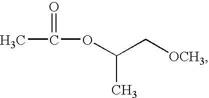
- the solvent is selected from a group consisting of propylene glycol monomethyl ether acetate (PGMEA), whose structure is shown below:
- IPA isopropanol
- DMF dimethylformamide
- a percentage of the solvent can be 78-94.18 percent by weight. When the percentage of the solvent is too high, a concentration of the solvent becomes so low that the thickness of the formed thin film is too thin to be even. When the percentage of the solvent is too low, the concentration of the solvent becomes so high that the thickness of the formed film is too thick.
- the dielectric layer can be applied to a field effect transistor and a thin film transistor (TFT) as a gate dielectric layer.
- TFT thin film transistor
- the dielectric layer can be applied to the insulating layer in the structure of metal layer-insulating layer-metal layer, such as a dielectric layer between two electrodes in a capacitor, but is not limited thereto.
- MIM metal layer-insulating layer-metal layer
- OTFT organic thin film transistor
- FIG. 1 is a schematic view of a structure of metal layer-insulating layer-metal layer.
- Materials of two metal layers 102 and 106 in an MIM structure 100 can be identical or different.
- the material of the metal layer 102 includes gold (Au), silver (Ag), aluminum (Al), copper (Cu), chromium (Cr) or a transparent conductive oxide, e.g., indium tin oxide (ITO).
- the material of the metal layer 106 may include Au, Ag, Al, Cu, Cr or a transparent conductive oxide, e.g., ITO.
- An insulating layer 104 is formed by polymerizing the composition for the photosensitive organic dielectric material of the present invention through irradiation.
- FIG. 2 is a schematic view of a top contact type OTFT structure.
- FIG. 3 is a schematic view of a bottom contact type OTFT structure.
- an OTFT 200 of the present invention has a gate 204 , a gate dielectric layer 206 , a source 210 , a drain 212 and an active layer 208 .
- the gate 204 can be disposed on a substrate 202 , and the gate dielectric layer 206 covers the gate 204 .
- the source 210 and the drain 212 are disposed on the gate dielectric layer 206 at two sides of the gate 204 .
- the active layer 208 is disposed over the gate 204 and under the source 210 and the drain 212 .
- the active layer 208 is disposed over the gate 204 and between the source 210 and the drain 212 and extends to cover upper portions of the source 210 and the drain 212 .
- a material of the substrate 202 is, for example, glass, plastic, metal or other suitable materials.
- the material of the gate 204 is, for example, metal, e.g., Au, Ag, Al, Cu, Cr, or a transparent conductive oxide, such as ITO.
- the material of the gate dielectric layer 206 is formed by polymerizing the composition for the photosensitive organic dielectric material through irradiation.
- the materials of the source 210 and the drain 212 include metal, e.g., Au, Ag, Al, Cu, Cr, or transparent conductive oxides, e.g., ITO.
- the material of the active layer 208 is, for example, pentacene, poly-(3-hexylthiophene) (P3HT), or tetracene.
- a manufacturing method of said OTFT includes first forming a gate 204 on a substrate 202 and then manufacturing a gate dielectric layer 206 with the composition of the present invention.
- a method for manufacturing the gate dielectric layer 206 may include first coating the composition for forming the photosensitive organic dielectric material on the substrate 202 according to the foregoing embodiment of the present invention. Afterwards, a baking process is performed to form a dielectric material layer. Finally, an exposure process and a developing process are performed to form the gate dielectric layer 206 .
- a coating method is spin coating, dip coating, or spray, for example.
- the baking process includes first performing a soft baking process at low temperature followed by a hard baking process at a higher temperature.
- the temperatures of the soft baking process and the hard baking process are related to the kind of solvent in the composition.
- the temperature for the soft baking process can be between a room temperature and 150° C., between the room temperature and 130° C., or between 50° C.
- a patterning method includes first performing an exposure process by using a photomask as a mask and without forming any photoresist layer on the dielectric material layer, for example.
- an area in the dielectric material layer not yet exposed is formed as an unexposed region, and an exposed area in the dielectric material layer is crosslinked and polymerized to form an exposed region.
- a developing process is performed to remove a dielectric material in the unexposed region of the dielectric material layer, leaving the remaining exposed region to form the gate dielectric layer 206 .
- a light source used in the exposure process is a mercury lamp, for example.
- An exposure intensity is, for example, 100-400 mJ/cm 2 .
- a developer solution used for the developing process is a water solution of tetra methyl ammonium hydroxide (TMAH) or a water solution of potassium hydroxide (KOH).
- the composition of the present invention may also be formed on the substrate 202 by direct patterning. Then, an irradiating process is performed followed by a baking process to polymerize the composition so as to form the gate dielectric layer 206 .
- the method for direct patterning includes, for example, slot die coating, flexographic coating, inkjet printing, microcontact printing, nanoimprinting, or screen printing.
- the patterned active layer 208 , the source 210 , and the drain 212 are further formed to accomplish the top contact type OTFT shown by FIG. 2 , or the bottom contact type OTFT shown by FIG. 3 .
- FIGS. 4A and 4B are electrical characteristic diagrams of a top contact type OTFT according to an embodiment of the present invention respectively.
- the ordinate represents a density of leakage current
- the abscissa represents an electric field intensity.
- the curve shows a relationship between a gate of the OTFT supplied with different voltages and the density of leakage current.
- Vg represents a voltage applied to the gate
- Id represents a corresponding current generated by a drain of the OTFT
- a curve shows the relationship between the voltage applied to the gate of the OTFT and the corresponding current generated by the drain of the OTFT.
- an electron mobility rate of the top contact type OTFT in the present embodiment is 0.66 cm 2 /V ⁇ s, and the density of leakage current is 2 ⁇ 10 ⁇ 8 A/cm 2 under the electric field of 2MV/cm.
- Embodiments disclosed herein may provide a composition for a photosensitive organic dielectric material.
- the composition is patterned by a wet developing process to form a gate organic dielectric layer so as to simplify the process.
- the composition for the photosensitive organic dielectric material has an extremely low density of leakage current.
- the photosensitive organic dielectric material when applied to top contact type OTFT devices, the photosensitive organic dielectric material also has satisfactory carrier mobility, and the process is suitable to be carried out at low temperature. Therefore, embodiments disclosed herein may provide not only has advantages such as implementation at low temperature and simplified process but is also applicable to device integration and mass production and thereby reducing the fabrication costs of the devices.
Landscapes
- Physics & Mathematics (AREA)
- General Physics & Mathematics (AREA)
- Spectroscopy & Molecular Physics (AREA)
- Thin Film Transistor (AREA)
Abstract
Description

derivatives thereof or a combination thereof. A molecular weight of polyvinyl phenol (PVA) can be 2000-40000. In the composition for forming the photosensitive organic dielectric material, a percentage of the polymer material can be 4-10 percent by weight. When the percentage of the polymer material is too high, a film thickness becomes too thick. Consequently, during operation, a smaller electric field is produced, and a higher voltage is required for operation. When the percentage of the polymer material is too low, the film thickness becomes too thin and tends to be uneven such that leakage current may occur during operation.

hexa methoxymethyl melamine-formaldehyde, or a combination thereof. In the composition for the photosensitive organic dielectric material, a percentage of the crosslinking agent can be 1.5-10 percent by weight. When the percentage of the crosslinking agent is too high, a crosslinking density becomes too high such that the formed thin film gets so rigid that it cracks easily, resulting in leakage current. When the percentage of the crosslinking agent is too low, a crosslinking density is insufficient such that leakage current occurs due to insufficient strength to withstand high voltages.

R1, R2 and R3 can be completely identical, partially identical or completely different, and they may respectively be a straight chain or a branched chain of alkyl group of C1-C4, arylene group, or arakyl group. X is a halogen, e.g., fluorine or chlorine. In the composition for the photosensitive organic dielectric material, a percentage of the photoacid generator can be 0.32-2 percent by weight. When the percentage of the photoacid generator is too high, so many ions are produced that a density of leakage current increases. When the percentage of the photoacid generator is too low, generated photoacid is insufficient such that an exposure process cannot be carried out to achieve perfectly developed patterns.

isopropanol (IPA), dimethylformamide (DMF), or a combination thereof. In the composition for the photosensitive organic dielectric material, a percentage of the solvent can be 78-94.18 percent by weight. When the percentage of the solvent is too high, a concentration of the solvent becomes so low that the thickness of the formed thin film is too thin to be even. When the percentage of the solvent is too low, the concentration of the solvent becomes so high that the thickness of the formed film is too thick.
Claims (18)


Applications Claiming Priority (3)
| Application Number | Priority Date | Filing Date | Title |
|---|---|---|---|
| TW97137953A | 2008-10-02 | ||
| TW097137953A TWI375119B (en) | 2008-10-02 | 2008-10-02 | Composition for forming photosensitive dielectric material and application thereof |
| TW97137953 | 2008-10-02 |
Publications (2)
| Publication Number | Publication Date |
|---|---|
| US20100084636A1 US20100084636A1 (en) | 2010-04-08 |
| US8288761B2 true US8288761B2 (en) | 2012-10-16 |
Family
ID=42075083
Family Applications (1)
| Application Number | Title | Priority Date | Filing Date |
|---|---|---|---|
| US12/426,295 Expired - Fee Related US8288761B2 (en) | 2008-10-02 | 2009-04-20 | Composition for photosensitive organic dielectric material and application thereof |
Country Status (2)
| Country | Link |
|---|---|
| US (1) | US8288761B2 (en) |
| TW (1) | TWI375119B (en) |
Families Citing this family (2)
| Publication number | Priority date | Publication date | Assignee | Title |
|---|---|---|---|---|
| US8692238B2 (en) | 2012-04-25 | 2014-04-08 | Eastman Kodak Company | Semiconductor devices and methods of preparation |
| CN106688050B (en) | 2014-06-11 | 2018-09-18 | 伊斯曼柯达公司 | The device of dielectric layer with band polymer containing thiosulfate |
Citations (2)
| Publication number | Priority date | Publication date | Assignee | Title |
|---|---|---|---|---|
| US20060145149A1 (en) * | 2003-08-29 | 2006-07-06 | Infineon Technologies Ag | Integrated circuit comprising an organic semiconductor, and method for the production of an integrated circuit |
| US20060202198A1 (en) * | 2003-08-29 | 2006-09-14 | Marcus Halik | Integrated circuit, and method for the production of an integrated circuit |
-
2008
- 2008-10-02 TW TW097137953A patent/TWI375119B/en not_active IP Right Cessation
-
2009
- 2009-04-20 US US12/426,295 patent/US8288761B2/en not_active Expired - Fee Related
Patent Citations (3)
| Publication number | Priority date | Publication date | Assignee | Title |
|---|---|---|---|---|
| US20060145149A1 (en) * | 2003-08-29 | 2006-07-06 | Infineon Technologies Ag | Integrated circuit comprising an organic semiconductor, and method for the production of an integrated circuit |
| US20060202198A1 (en) * | 2003-08-29 | 2006-09-14 | Marcus Halik | Integrated circuit, and method for the production of an integrated circuit |
| US20080315192A1 (en) * | 2003-08-29 | 2008-12-25 | Marcus Halik | Integrated Circuit Comprising an Organic Semiconductor, and Method for the Production of an Integrated Circuit |
Also Published As
| Publication number | Publication date |
|---|---|
| TWI375119B (en) | 2012-10-21 |
| TW201015215A (en) | 2010-04-16 |
| US20100084636A1 (en) | 2010-04-08 |
Similar Documents
| Publication | Publication Date | Title |
|---|---|---|
| JP4629997B2 (en) | Thin film transistor and thin film transistor array | |
| KR101186740B1 (en) | Method for Fabricating Bank and Organic Thin Film Transistor Having the Bank | |
| JP5221896B2 (en) | Electrode forming method for organic electronic device, organic thin film transistor including electrode formed thereby, and display device having the same | |
| KR101467507B1 (en) | Organic thin film transistors | |
| US7834352B2 (en) | Method of fabricating thin film transistor | |
| JP4439394B2 (en) | Pattern formation method | |
| CN104377311B (en) | Hydrophobic cofferdam | |
| JP2010532559A (en) | Self-aligned organic thin film transistor and method for manufacturing the same | |
| US20150364685A1 (en) | Process for patterning materials in thin-film devices | |
| US10707079B2 (en) | Orthogonal patterning method | |
| JP2004234901A (en) | Display substrate, organic EL display device, display substrate manufacturing method and electronic device | |
| CN101384963A (en) | A method of patterning a thin film | |
| JP6635041B2 (en) | Thin-film transistors and MOS field-effect transistors using repellent materials and methods of manufacturing the same | |
| WO2015076334A1 (en) | Transistor manufacturing method and transistor | |
| JP4572501B2 (en) | Method for producing organic thin film transistor | |
| US8288761B2 (en) | Composition for photosensitive organic dielectric material and application thereof | |
| US20170194583A1 (en) | Method of manufacturing thin film transistor, thin film transistor manufactured by the method, and electronic device comprising the thin film transistor | |
| JP5332145B2 (en) | Multilayer structure, electronic device, electronic device array, and display device | |
| TWI469224B (en) | Organic thin film transistor and fabricating the same | |
| KR101249097B1 (en) | Composition for Organic Gate Insulator, Method for Fabricating Organic Gate Insulator and Organic Thin Film Transistor Having the Same | |
| JP2007227595A (en) | Method for producing organic thin film transistor | |
| JP4906934B2 (en) | Electronic element, electronic element array, and display device | |
| KR100546065B1 (en) | Water soluble photoresist, organic thin film photolithography process and organic thin film shaping process | |
| TW201830746A (en) | Polar elastomer microstructures and methods for fabricating same |
Legal Events
| Date | Code | Title | Description |
|---|---|---|---|
| AS | Assignment |
Owner name: INDUSTRIAL TECHNOLOGY RESEARCH INSTITUTE,TAIWAN Free format text: ASSIGNMENT OF ASSIGNORS INTEREST;ASSIGNORS:LIN, MEI-RU;YAN, JING-YI;CHEN, LIANG-HSIANG;AND OTHERS;REEL/FRAME:022617/0010 Effective date: 20090109 Owner name: INDUSTRIAL TECHNOLOGY RESEARCH INSTITUTE, TAIWAN Free format text: ASSIGNMENT OF ASSIGNORS INTEREST;ASSIGNORS:LIN, MEI-RU;YAN, JING-YI;CHEN, LIANG-HSIANG;AND OTHERS;REEL/FRAME:022617/0010 Effective date: 20090109 |
|
| STCF | Information on status: patent grant |
Free format text: PATENTED CASE |
|
| FPAY | Fee payment |
Year of fee payment: 4 |
|
| FEPP | Fee payment procedure |
Free format text: MAINTENANCE FEE REMINDER MAILED (ORIGINAL EVENT CODE: REM.); ENTITY STATUS OF PATENT OWNER: LARGE ENTITY |
|
| LAPS | Lapse for failure to pay maintenance fees |
Free format text: PATENT EXPIRED FOR FAILURE TO PAY MAINTENANCE FEES (ORIGINAL EVENT CODE: EXP.); ENTITY STATUS OF PATENT OWNER: LARGE ENTITY |
|
| STCH | Information on status: patent discontinuation |
Free format text: PATENT EXPIRED DUE TO NONPAYMENT OF MAINTENANCE FEES UNDER 37 CFR 1.362 |
|
| FP | Lapsed due to failure to pay maintenance fee |
Effective date: 20201016 |