US8259243B2 - Controllable device for phase modulation - Google Patents
Controllable device for phase modulation Download PDFInfo
- Publication number
- US8259243B2 US8259243B2 US12/466,433 US46643309A US8259243B2 US 8259243 B2 US8259243 B2 US 8259243B2 US 46643309 A US46643309 A US 46643309A US 8259243 B2 US8259243 B2 US 8259243B2
- Authority
- US
- United States
- Prior art keywords
- modulator
- phase
- liquid crystal
- controllable
- cells
- Prior art date
- Legal status (The legal status is an assumption and is not a legal conclusion. Google has not performed a legal analysis and makes no representation as to the accuracy of the status listed.)
- Active, expires
Links
- 239000004973 liquid crystal related substance Substances 0.000 claims abstract description 114
- 239000011159 matrix material Substances 0.000 claims abstract description 43
- 230000001427 coherent effect Effects 0.000 claims abstract description 9
- 210000004027 cell Anatomy 0.000 claims description 102
- 230000003287 optical effect Effects 0.000 claims description 22
- 239000000463 material Substances 0.000 claims description 14
- 239000006185 dispersion Substances 0.000 claims description 10
- 239000003086 colorant Substances 0.000 claims description 8
- 230000005684 electric field Effects 0.000 claims description 5
- 239000004990 Smectic liquid crystal Substances 0.000 claims description 3
- 239000000203 mixture Substances 0.000 claims description 3
- 210000002858 crystal cell Anatomy 0.000 claims description 2
- 230000010287 polarization Effects 0.000 claims 1
- 230000008859 change Effects 0.000 description 8
- 230000000694 effects Effects 0.000 description 8
- 230000006870 function Effects 0.000 description 8
- 230000001934 delay Effects 0.000 description 5
- 238000000034 method Methods 0.000 description 5
- 230000008901 benefit Effects 0.000 description 4
- 230000010363 phase shift Effects 0.000 description 4
- 238000001311 chemical methods and process Methods 0.000 description 3
- 230000000630 rising effect Effects 0.000 description 3
- 230000003068 static effect Effects 0.000 description 3
- 230000002411 adverse Effects 0.000 description 2
- 238000004519 manufacturing process Methods 0.000 description 2
- 238000012986 modification Methods 0.000 description 2
- 230000004048 modification Effects 0.000 description 2
- 239000013642 negative control Substances 0.000 description 2
- 239000013641 positive control Substances 0.000 description 2
- 230000008569 process Effects 0.000 description 2
- 230000003595 spectral effect Effects 0.000 description 2
- 239000000126 substance Substances 0.000 description 2
- 239000000758 substrate Substances 0.000 description 2
- 230000006399 behavior Effects 0.000 description 1
- 230000006835 compression Effects 0.000 description 1
- 238000007906 compression Methods 0.000 description 1
- 239000013078 crystal Substances 0.000 description 1
- 230000001419 dependent effect Effects 0.000 description 1
- 238000005516 engineering process Methods 0.000 description 1
- 230000008571 general function Effects 0.000 description 1
- 239000011521 glass Substances 0.000 description 1
- ORUIBWPALBXDOA-UHFFFAOYSA-L magnesium fluoride Chemical compound [F-].[F-].[Mg+2] ORUIBWPALBXDOA-UHFFFAOYSA-L 0.000 description 1
- 229910001635 magnesium fluoride Inorganic materials 0.000 description 1
- 230000001902 propagating effect Effects 0.000 description 1
- 239000010453 quartz Substances 0.000 description 1
- VYPSYNLAJGMNEJ-UHFFFAOYSA-N silicon dioxide Inorganic materials O=[Si]=O VYPSYNLAJGMNEJ-UHFFFAOYSA-N 0.000 description 1
- 238000001228 spectrum Methods 0.000 description 1
- 230000001360 synchronised effect Effects 0.000 description 1
- 238000002834 transmittance Methods 0.000 description 1
Images


Classifications
-
- G—PHYSICS
- G03—PHOTOGRAPHY; CINEMATOGRAPHY; ANALOGOUS TECHNIQUES USING WAVES OTHER THAN OPTICAL WAVES; ELECTROGRAPHY; HOLOGRAPHY
- G03H—HOLOGRAPHIC PROCESSES OR APPARATUS
- G03H1/00—Holographic processes or apparatus using light, infrared or ultraviolet waves for obtaining holograms or for obtaining an image from them; Details peculiar thereto
- G03H1/02—Details of features involved during the holographic process; Replication of holograms without interference recording
-
- G—PHYSICS
- G09—EDUCATION; CRYPTOGRAPHY; DISPLAY; ADVERTISING; SEALS
- G09G—ARRANGEMENTS OR CIRCUITS FOR CONTROL OF INDICATING DEVICES USING STATIC MEANS TO PRESENT VARIABLE INFORMATION
- G09G3/00—Control arrangements or circuits, of interest only in connection with visual indicators other than cathode-ray tubes
- G09G3/001—Control arrangements or circuits, of interest only in connection with visual indicators other than cathode-ray tubes using specific devices not provided for in groups G09G3/02 - G09G3/36, e.g. using an intermediate record carrier such as a film slide; Projection systems; Display of non-alphanumerical information, solely or in combination with alphanumerical information, e.g. digital display on projected diapositive as background
- G09G3/003—Control arrangements or circuits, of interest only in connection with visual indicators other than cathode-ray tubes using specific devices not provided for in groups G09G3/02 - G09G3/36, e.g. using an intermediate record carrier such as a film slide; Projection systems; Display of non-alphanumerical information, solely or in combination with alphanumerical information, e.g. digital display on projected diapositive as background to produce spatial visual effects
-
- G—PHYSICS
- G02—OPTICS
- G02F—OPTICAL DEVICES OR ARRANGEMENTS FOR THE CONTROL OF LIGHT BY MODIFICATION OF THE OPTICAL PROPERTIES OF THE MEDIA OF THE ELEMENTS INVOLVED THEREIN; NON-LINEAR OPTICS; FREQUENCY-CHANGING OF LIGHT; OPTICAL LOGIC ELEMENTS; OPTICAL ANALOGUE/DIGITAL CONVERTERS
- G02F1/00—Devices or arrangements for the control of the intensity, colour, phase, polarisation or direction of light arriving from an independent light source, e.g. switching, gating or modulating; Non-linear optics
- G02F1/01—Devices or arrangements for the control of the intensity, colour, phase, polarisation or direction of light arriving from an independent light source, e.g. switching, gating or modulating; Non-linear optics for the control of the intensity, phase, polarisation or colour
- G02F1/13—Devices or arrangements for the control of the intensity, colour, phase, polarisation or direction of light arriving from an independent light source, e.g. switching, gating or modulating; Non-linear optics for the control of the intensity, phase, polarisation or colour based on liquid crystals, e.g. single liquid crystal display cells
- G02F1/133—Constructional arrangements; Operation of liquid crystal cells; Circuit arrangements
- G02F1/1333—Constructional arrangements; Manufacturing methods
- G02F1/1335—Structural association of cells with optical devices, e.g. polarisers or reflectors
- G02F1/13363—Birefringent elements, e.g. for optical compensation
- G02F1/133638—Waveplates, i.e. plates with a retardation value of lambda/n
-
- G—PHYSICS
- G02—OPTICS
- G02F—OPTICAL DEVICES OR ARRANGEMENTS FOR THE CONTROL OF LIGHT BY MODIFICATION OF THE OPTICAL PROPERTIES OF THE MEDIA OF THE ELEMENTS INVOLVED THEREIN; NON-LINEAR OPTICS; FREQUENCY-CHANGING OF LIGHT; OPTICAL LOGIC ELEMENTS; OPTICAL ANALOGUE/DIGITAL CONVERTERS
- G02F1/00—Devices or arrangements for the control of the intensity, colour, phase, polarisation or direction of light arriving from an independent light source, e.g. switching, gating or modulating; Non-linear optics
- G02F1/01—Devices or arrangements for the control of the intensity, colour, phase, polarisation or direction of light arriving from an independent light source, e.g. switching, gating or modulating; Non-linear optics for the control of the intensity, phase, polarisation or colour
- G02F1/13—Devices or arrangements for the control of the intensity, colour, phase, polarisation or direction of light arriving from an independent light source, e.g. switching, gating or modulating; Non-linear optics for the control of the intensity, phase, polarisation or colour based on liquid crystals, e.g. single liquid crystal display cells
- G02F1/137—Devices or arrangements for the control of the intensity, colour, phase, polarisation or direction of light arriving from an independent light source, e.g. switching, gating or modulating; Non-linear optics for the control of the intensity, phase, polarisation or colour based on liquid crystals, e.g. single liquid crystal display cells characterised by the electro-optical or magneto-optical effect, e.g. field-induced phase transition, orientation effect, guest-host interaction or dynamic scattering
- G02F1/13781—Devices or arrangements for the control of the intensity, colour, phase, polarisation or direction of light arriving from an independent light source, e.g. switching, gating or modulating; Non-linear optics for the control of the intensity, phase, polarisation or colour based on liquid crystals, e.g. single liquid crystal display cells characterised by the electro-optical or magneto-optical effect, e.g. field-induced phase transition, orientation effect, guest-host interaction or dynamic scattering using smectic liquid crystals
-
- G—PHYSICS
- G02—OPTICS
- G02F—OPTICAL DEVICES OR ARRANGEMENTS FOR THE CONTROL OF LIGHT BY MODIFICATION OF THE OPTICAL PROPERTIES OF THE MEDIA OF THE ELEMENTS INVOLVED THEREIN; NON-LINEAR OPTICS; FREQUENCY-CHANGING OF LIGHT; OPTICAL LOGIC ELEMENTS; OPTICAL ANALOGUE/DIGITAL CONVERTERS
- G02F2203/00—Function characteristic
- G02F2203/04—Function characteristic wavelength independent
-
- G—PHYSICS
- G02—OPTICS
- G02F—OPTICAL DEVICES OR ARRANGEMENTS FOR THE CONTROL OF LIGHT BY MODIFICATION OF THE OPTICAL PROPERTIES OF THE MEDIA OF THE ELEMENTS INVOLVED THEREIN; NON-LINEAR OPTICS; FREQUENCY-CHANGING OF LIGHT; OPTICAL LOGIC ELEMENTS; OPTICAL ANALOGUE/DIGITAL CONVERTERS
- G02F2203/00—Function characteristic
- G02F2203/12—Function characteristic spatial light modulator
-
- G—PHYSICS
- G02—OPTICS
- G02F—OPTICAL DEVICES OR ARRANGEMENTS FOR THE CONTROL OF LIGHT BY MODIFICATION OF THE OPTICAL PROPERTIES OF THE MEDIA OF THE ELEMENTS INVOLVED THEREIN; NON-LINEAR OPTICS; FREQUENCY-CHANGING OF LIGHT; OPTICAL LOGIC ELEMENTS; OPTICAL ANALOGUE/DIGITAL CONVERTERS
- G02F2203/00—Function characteristic
- G02F2203/50—Phase-only modulation
-
- G—PHYSICS
- G02—OPTICS
- G02F—OPTICAL DEVICES OR ARRANGEMENTS FOR THE CONTROL OF LIGHT BY MODIFICATION OF THE OPTICAL PROPERTIES OF THE MEDIA OF THE ELEMENTS INVOLVED THEREIN; NON-LINEAR OPTICS; FREQUENCY-CHANGING OF LIGHT; OPTICAL LOGIC ELEMENTS; OPTICAL ANALOGUE/DIGITAL CONVERTERS
- G02F2413/00—Indexing scheme related to G02F1/13363, i.e. to birefringent elements, e.g. for optical compensation, characterised by the number, position, orientation or value of the compensation plates
- G02F2413/02—Number of plates being 2
-
- G—PHYSICS
- G03—PHOTOGRAPHY; CINEMATOGRAPHY; ANALOGOUS TECHNIQUES USING WAVES OTHER THAN OPTICAL WAVES; ELECTROGRAPHY; HOLOGRAPHY
- G03H—HOLOGRAPHIC PROCESSES OR APPARATUS
- G03H1/00—Holographic processes or apparatus using light, infrared or ultraviolet waves for obtaining holograms or for obtaining an image from them; Details peculiar thereto
- G03H1/22—Processes or apparatus for obtaining an optical image from holograms
- G03H1/2294—Addressing the hologram to an active spatial light modulator
-
- G—PHYSICS
- G03—PHOTOGRAPHY; CINEMATOGRAPHY; ANALOGOUS TECHNIQUES USING WAVES OTHER THAN OPTICAL WAVES; ELECTROGRAPHY; HOLOGRAPHY
- G03H—HOLOGRAPHIC PROCESSES OR APPARATUS
- G03H1/00—Holographic processes or apparatus using light, infrared or ultraviolet waves for obtaining holograms or for obtaining an image from them; Details peculiar thereto
- G03H1/02—Details of features involved during the holographic process; Replication of holograms without interference recording
- G03H2001/0208—Individual components other than the hologram
- G03H2001/0224—Active addressable light modulator, i.e. Spatial Light Modulator [SLM]
-
- G—PHYSICS
- G03—PHOTOGRAPHY; CINEMATOGRAPHY; ANALOGOUS TECHNIQUES USING WAVES OTHER THAN OPTICAL WAVES; ELECTROGRAPHY; HOLOGRAPHY
- G03H—HOLOGRAPHIC PROCESSES OR APPARATUS
- G03H2225/00—Active addressable light modulator
- G03H2225/30—Modulation
- G03H2225/32—Phase only
-
- G—PHYSICS
- G03—PHOTOGRAPHY; CINEMATOGRAPHY; ANALOGOUS TECHNIQUES USING WAVES OTHER THAN OPTICAL WAVES; ELECTROGRAPHY; HOLOGRAPHY
- G03H—HOLOGRAPHIC PROCESSES OR APPARATUS
- G03H2240/00—Hologram nature or properties
- G03H2240/20—Details of physical variations exhibited in the hologram
- G03H2240/40—Dynamic of the variations
- G03H2240/42—Discrete level
-
- G—PHYSICS
- G09—EDUCATION; CRYPTOGRAPHY; DISPLAY; ADVERTISING; SEALS
- G09G—ARRANGEMENTS OR CIRCUITS FOR CONTROL OF INDICATING DEVICES USING STATIC MEANS TO PRESENT VARIABLE INFORMATION
- G09G3/00—Control arrangements or circuits, of interest only in connection with visual indicators other than cathode-ray tubes
- G09G3/20—Control arrangements or circuits, of interest only in connection with visual indicators other than cathode-ray tubes for presentation of an assembly of a number of characters, e.g. a page, by composing the assembly by combination of individual elements arranged in a matrix no fixed position being assigned to or needed to be assigned to the individual characters or partial characters
- G09G3/34—Control arrangements or circuits, of interest only in connection with visual indicators other than cathode-ray tubes for presentation of an assembly of a number of characters, e.g. a page, by composing the assembly by combination of individual elements arranged in a matrix no fixed position being assigned to or needed to be assigned to the individual characters or partial characters by control of light from an independent source
- G09G3/36—Control arrangements or circuits, of interest only in connection with visual indicators other than cathode-ray tubes for presentation of an assembly of a number of characters, e.g. a page, by composing the assembly by combination of individual elements arranged in a matrix no fixed position being assigned to or needed to be assigned to the individual characters or partial characters by control of light from an independent source using liquid crystals
- G09G3/3611—Control of matrices with row and column drivers
Definitions
- the present invention relates to a device for phase modulation of coherent light with a spatial light modulator which comprises a modulator matrix with a regular arrangement of controllable LC modulator cells, with at least one light source which illuminates the modulator matrix, and with a control unit which controls the phase modulation in the LC modulator cells.
- a spatial light modulator which comprises a modulator matrix with a regular arrangement of controllable LC modulator cells, with at least one light source which illuminates the modulator matrix, and with a control unit which controls the phase modulation in the LC modulator cells.
- the field of application of this invention includes coherent-optical applications which comprise for modulating coherent light a liquid crystal (LC) device which is used to control the phase of the light in phase steps, whose number typically ranges between more than fifty and several hundreds, in a modulation element of the LC device.
- the LC device can be used for three-dimensional, preferably holographic image representation.
- LC SLM spatial light modulator
- the switching delay of the LC molecules in a LC SLM depends among other factors on the LC type (nematic, smectic, . . . ) and on the arrangement of the LC molecules in a modulator cell of the modulator matrix of the LC SLM.
- Frame inversion is realised in one embodiment such that in a first frame all modulator cells of the modulator matrix are controlled with a positive voltage and in a second frame all modulator cells of the modulator matrix are controlled with a negative voltage.
- the sign of the voltage can be altered dot-wise (‘dot inversion’) or line-wise (‘line inversion’) in order to prevent flickering.
- dot inversion in a first frame even columns of the modulator matrix are controlled with a positive voltage and odd columns are controlled with a negative voltage, for example. In a second frame, the columns are controlled vice versa.
- dot inversion the modulator matrix shows a chessboard-like pattern of positive and negative control voltages.
- the orientation of the LC molecules depends only on the absolute value of the applied voltage, not on the sign. The orientation of these LC molecules does thus not change when frame inversion is employed.
- IPS in-plane switching
- Physical modifications of known, commercially available LC SLM should preferably be as little as possible to achieve the aforementioned goals.
- the object can be solved by a device for phase modulation of coherent light with a spatial light modulator comprising a modulator matrix with a regular arrangement of controllable LC modulator cells, with at least one light source which illuminates the modulator matrix, and with a control unit that can control the phase modulation in the LC modulator cells, to realise a three-dimensional image representation in a display device comprising the modulation device.
- a device for phase modulation of coherent light with a spatial light modulator comprising a modulator matrix with a regular arrangement of controllable LC modulator cells, with at least one light source which illuminates the modulator matrix, and with a control unit that can control the phase modulation in the LC modulator cells, to realise a three-dimensional image representation in a display device comprising the modulation device.
- the device according to this invention can be further configured such that
- the LC material can be used as a controllable ⁇ /2 plate because the birefringence of the LC material and the layer thickness are matched accordingly.
- a change in the sign of the applied voltage effects a different orientation of the LC molecules in PSS LC cells, as described above.
- This change in molecule orientation corresponds with a rotation of the optical axis of the ⁇ /2 plate.
- the molecule orientation and the optical axis are turned clockwise in order to realise positive voltages, and counter-clockwise to realise negative voltages.
- phase-modulating light modulator In contrast to an amplitude-modulating light modulator, in a phase-modulating light modulator of the above-described configuration the phase conditions change depending on the sign of the applied voltage.
- the ⁇ /2 plate disposed between two ⁇ /4 plates turning the optical axis of the ⁇ /2 plate clockwise corresponds to a phase shift with positive sign, turning it counter-clockwise corresponds to a phase shift with negative sign.
- a modulator cell is controlled e.g. by a voltage U 0 with positive sign, and if this voltage corresponds to a rotation angle of the optical axis ⁇ 0 and a phase + ⁇ 0 , then if the same modulator cell is controlled with the voltage ⁇ U 0 with the same absolute value but negative sign the rotation angle of the optical axis is ⁇ 0 and the phase is ⁇ 0 , i.e. with the same absolute value but opposite sign.
- phase modulation in a large modulation range of phase values it is therefore necessary to modify the control method such that the sign of the voltage can be chosen individually for each modulator cell, depending on the actual phase value to be written. This doubles the phase range which can be realised compared with the case where only control voltages with one sign can be used.
- phase values are here adapted in every other frame. This is done for example in that the same information is written with the help of control signals generated by the control unit, but while the image content is the same, different signs of the voltage are generated simultaneously for individual modulator cells in every other frame.
- phase offset of the phase values to be written is permitted for the entire modulator matrix. This means that a constant phase value is added simultaneously for each modulator cell. In most coherent applications, e.g. for hologram reconstructions, it is only the relative phase between individual modulator cells of the PSS LC SLM that matters, not the absolute phase. This is why the phase offset can be employed advantageously here.
- Frame inversion can thus be replaced equivalently as follows: In every other frame the phase values to be written to the LC SLM are given a globally constant phase offset (modulo 2 ⁇ ), where the amount of the offset depends on the modulation range of the SLM.
- the preferred phase offset is ⁇ for a modulator with a modulation range of 2 ⁇ .
- a phase-modulating light modulator has a relative phase of 0 at a voltage of 0; it shows a phase shift of + ⁇ at a maximum positive control voltage U max . Consequently, at the negative control voltage ⁇ U max the phase shift is ⁇ , relative to the voltage 0.
- the phase-modulating light modulator thus has a modulation range of 2 ⁇ , namely the range [ ⁇ . . . + ⁇ ].
- the sub-range [ ⁇ . . . 0] corresponds with negative voltages
- the sub-range [0 . . . + ⁇ ] corresponds with positive voltages.
- the phase pattern is linear rising because the difference between values written to adjacent cells is always ⁇ /4.
- these two modulator cells are controlled with negative voltages.
- the third cell would be controlled with the voltage 0 and the fourth with a positive voltage.
- phase value modulo 2 ⁇ is relevant for the representation of a complex number.
- the sub-range [ ⁇ . . . 0] is thus equivalent to the shifted range [ ⁇ . . . 2 ⁇ ].
- the sign of the control voltage thus changes for all modulator cells but the third one, which forms an exception because its control voltage is zero in one frame. However, it is still the same phase pattern, namely the linear rising phase, that is written to the modulator cells. This means that the difference between the phase values of adjacent cells also remains ⁇ /4 in the second frame. It is thus achieved that the sign of the voltage is inverted in most cells in every other frame according to the phase value setting, while the relevant phase pattern which is written to the modulator matrix remains the same.
- the local phase offset can be generated in the LC modulator cells while the electric field is turned off by aligning the molecule axes of the LC molecules parallel with the optical axes of the ⁇ /4 layers.
- phase value which results from a given voltage can be realised in a LC modulator cell with same absolute value but opposite sign when the voltage polarity is reversed.
- the at least one light source of the controllable device is preferably designed for providing polarised light.
- the modulator matrix can alternatively comprise at least one entry-side polariser.
- the polariser can preferably be a circular polariser, which combines the functionality of a ⁇ /4 plate and a linear polariser.
- the modulator matrix has such a configuration of the ⁇ /4 plates and/or ⁇ /2 plate that a phase modulation can be controlled by the control unit for at least three different colours or wavelengths.
- the LC layer of the ⁇ /2 plate has a thickness d which is optimised for the central one of the at least three wavelengths which are modulated.
- the device for phase modulation can comprise LC modulator cells with a mix of LC materials whose dispersion changes with the wavelength, so that ⁇ n ( ⁇ ) d ⁇ /2 applies for the different wavelengths of the at least three colours.
- the ⁇ /4 plates and/or the ⁇ /2 plate show a different layer thickness d and/or orientation of their optical axes for the LC modulator cells which correspond with the different wavelengths.
- the non-controllable ⁇ /4 plates can be achromatic elements. The physical form of these ⁇ /4 plates and that of the achromatic circular polarisers, into which the functionality of the ⁇ /4 plates is integrated, can be the same as explained in the description of the prior art.
- a device for phase modulation with the physical forms described above can preferably be provided by relatively simple but effective modifications of a prior art LC SLM which boasts short switching delays.
- FIG. 1 is a schematic view of a LC arrangement for phase modulation according to this invention
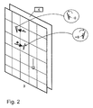
- FIG. 2 is a schematic view of the preferred direction of rotation of the LC molecules depending on the applied voltage
- FIGS. 3 a , 3 b are schematic views of a modulator matrix with an inversion of the LC modulator cells in two subsequent frames according to the prior art
- FIGS. 4 a , 4 b are schematic views of a modulator matrix with individually locally controlled LC modulator cells ( FIG. 4 a ) and with the inversion of the LC modulator cells caused by a global phase offset ( FIG. 4 b ).
- the inventive device for phase modulation of coherent light comprises a spatial light modulator (SLM), at least one light source means for illuminating the modulator matrix of the SLM, and a control unit for controlling the phase modulation of modulator cells of the modulator matrix.
- the modulator cells are LC modulator cells which are arranged regularly in rows and columns and which are preferably of rectangular shape.
- the function of the invention can also be realised with other forms of LC modulator cells.
- the control unit comprises memory units and computing units which communicate with each other with the help of software and hardware elements in order to generate and exchange data in order to control the LC modulator cells with control signals for a preferably three-dimensional image representation.
- the device for phase modulation can for example be integrated into a holographic display device.
- FIG. 1 The design of a controllable phase-modulating device is shown schematically in FIG. 1 with its major components.
- a three-dimensional modulator matrix 3 with a layer thickness d forms a controllable ⁇ /2 plate, and is disposed between two static, non-controllable layers.
- the two static layers have the function of non-controllable ⁇ /4 plates 2 , 2 ′.
- this is the same arrangement as described by Pancharatnam [2] in the prior art section.
- the ⁇ /4 plates 2 , 2 ′ can for example be realised in the form of films.
- the ⁇ /2 plate comprises a LC layer of the PSS liquid crystal type, which can be controlled by a control unit 4 , and shows a regular arrangement of modulator cells in rows and columns.
- An oriented LC molecule is shown exemplarily in the drawing in several modulator cells.
- the optical axes of the two ⁇ /4 plates 2 , 2 ′ are parallel, they are indicated by a vertical line.
- the numerals 1 and 1 ′ designate the polarisation direction of the incident light at the points of entry and exit of the modulation device.
- the thickness d of the LC layer is such to provide the functionality of a ⁇ /2 plate, it is characterised by the equation (1) ⁇ n d ⁇ (2m+1) ⁇ /2,
- ⁇ n describes the birefringence of the LC material used
- ⁇ is the wavelength of the used light
- m is an integer number.
- the orientation of the ⁇ /4 plates 2 , 2 ′ relative to the orientation of the birefringent LC molecules when no electric field is applied is here chosen such that the optical axes of the ⁇ /4 plates and that of the ⁇ /2 plate are parallel. It is generally also possible to use other mutual orientations of the optical axes.
- Light 1 which is emitted by a light source means (not shown), and which is preferably linear polarised, falls on the non-controllable ⁇ /4 plate 2 with a polarisation angle ⁇ of 45°.
- This ⁇ /4 plate transforms the linear polarised light into circular polarised light.
- the controllable ⁇ /2 plate which follows in the direction of the propagating incident light, modulates the phase of the passing light depending on the actually set rotation angle of its optical axis.
- the shown parallel orientation of the optical axes is considered to be the relative phase 0 . Controlling the ⁇ /2 plate would result in a phase change.
- the second ⁇ /4 plate 2 ′ which follows the ⁇ /2 plate, then generates linear polarised light 1 ′ again with a polarisation direction which is parallel to that on the entry side.
- the at least one light source can for example be a laser which preferably generates linear polarised light.
- the arrangement shown in FIG. 1 can also comprise at least one linear polariser which can be additionally activated.
- Another possibility of generating a global phase offset is to use commercially available circular polarisers, which already combine the functions of a linear polariser and a ⁇ /4 plate.
- Prior art LC light modulators are often designed such that there are at least two substrates—commonly in the form of thin glass plates—on either side of the LC layer.
- One substrate typically accommodates a common electrode (basic electrode) for all modulator cells, and the other substrate accommodates an individual electrode for controlling each modulator cell.
- the devices are controlled in that the common electrode is given a mean voltage different from zero, e.g. 6 V (also known as source bus voltage).
- the individual electrodes can then be given higher or lower variable voltage values, e.g. 9 V for one modulator cell and 3 V for another cell.
- the voltage values activated from outside are positive.
- the liquid crystals of the modulator matrix only change their orientation depending on the absolute value of the voltage, but not on its sign. In these types of modulators, changing the sign does therefore not have any adverse effects on the orientation of the liquid crystal molecules.
- PSS LCD PSS liquid crystal type
- FIG. 2 This is shown schematically in FIG. 2 .
- the modulator matrix 3 which is shown in a perspective view, there are three modulator cells with one LC molecule each with its orientation when voltage is applied; arrows indicate these oriented molecules.
- the LC molecules rotate counter-clockwise by the angle ⁇ .
- the LC molecules rotate clockwise by the angle + ⁇ .
- the voltage value 0 is shown in a third modulator cell (right-hand side of the matrix) for comparison.
- a PSS LCD is used as an amplitude-modulating display, controlling the cells with different signs always causes the same amplitude. This is because the amplitude control is based on a rotation of linear polarised light. A ⁇ /2 plate with an angle ⁇ relative to the polarisation of the incident light turns it by 2 ⁇ . The transmittance of the amplitude-modulating light modulator with crossed polarisers is proportional to the square sine of 2 ⁇ . It is thus the same for the positive angle 2 ⁇ and for the negative angle ⁇ 2 ⁇ . Consequently, in a display device or modulator matrix it is irrelevant whether the molecules rotate clockwise or counter-clockwise. If an amplitude-modulating light modulator is realised with a PSS LCD, the device can thus be controlled conventionally.
- phase value created by a positive voltage would differ from that created by a negative voltage.
- the electric control by the control unit must be adapted according to this invention such that an individual modulator cell can be controlled locally with either a positive or a negative voltage.
- the control unit In order to be able to realise a phase modulation in the positive range of values of 0 . . . + ⁇ , the control unit must control the modulator cells of the modulator matrix 3 with a positive voltage value, so that the LC molecules rotate clockwise. If the modulator cells are controlled with a negative voltage value of the same magnitude, so that the LC molecules rotate counter-clockwise, the phase will be modulated in the negative range of values of 0 . . . ⁇ . Due to the fact that for representing complex numbers phase values only enter modulo 2 ⁇ , the negative value ⁇ is equivalent to 2 ⁇ .
- FIGS. 3 a and 3 b illustrate schematically a conventional control of a SLM according to the prior art, showing the principle of the pixel inversion for two subsequent frames M and M+1.
- the SLM comprise a modulator matrix with 4 ⁇ 4 modulator cells which are regularly arranged in rows and columns.
- the individual signs of the voltages for each of the 4 ⁇ 4 modulator cells are inverted compared with frame M.
- the inversion shown here takes advantage of a chessboard-like pattern for controlling the cells.
- the modulator cells can also be controlled by the control unit in different patterns. For example, every other column in frame M could be controlled only with negative or only with positive voltage values. Or all modulator cells in frame M could be controlled with positive voltage values, and in frame M+1 with negative voltage values.
- control means control each modulator cell individually locally with a positive or negative voltage, according to the given phase value to be written. This is shown in an embodiment of the SLM shown in FIGS. 4 a and 4 b.
- a numerical example (1) shows for a SLM made up of 4 ⁇ 4 modulator cells for phase modulation phase values to be written between 0 and 2 ⁇ for a linear phase pattern.
- the phase values are for example pre-computed and stored in memory units of the control unit.
- FIG. 4 a shows schematically the modulator cells to be controlled with positive and negative voltage values, represented by plus and minus signs in the respective cell. All modulator cells with phase values in the range [0 . . . ⁇ ] are controlled with a positive voltage. All phase values in the range [ ⁇ . . . 2 ⁇ ] are controlled with negative voltage values, because the range [ ⁇ . . . 2 ⁇ ] is equivalent to the range ⁇ [ ⁇ . . . 0] for a modulo 2 ⁇ representation.
- the left modulator cell in the top row with the phase 0.7 ⁇ is for example controlled with a voltage U 1
- the individual local control of the modulator cells with positive and negative voltage values causes the aforementioned problem of the occurrence of disturbing chemical processes when a DC voltage is applied for a long time, i.e. if the same content is to be displayed for a long time.
- the same phase values must be written to the same modulator cells several times.
- phase offset is introduced between subsequently displayed frames for the entire modulator matrix, in order to overcome this problem.
- This phase offset is generated by the control unit, or is directly integrated into a computation, for example a hologram computation.
- the idea to use a phase offset is based on the finding that only the relative phase between individual modulator cells matters for the function as a phase-modulating light modulator in coherent-optical applications, but not the absolute phase of the individual cells.
- the sign is inverted in each modulator cell.
- the control voltage for the left cell in the first row changed for example from 0.7 ⁇ (positive voltage) in numerical example (1) to 1.7 ⁇ (i.e. 2 ⁇ 0.3 ⁇ , negative voltage) in numerical example (2).
- the global phase offset can be realised in different ways in the device for phase modulation.
- One possibility is to process the phase offset in the computing unit for generating the data to be written to the light modulator, e.g. during a hologram computation.
- An electric control voltage is calculated in the control unit for each modulator cell in the SLM to be controlled depending on the phase value to be written.
- a further possibility of realising a global phase offset is thus for the control unit to take into account the phase offset when calculating the control voltage in every other frame.
- the mean voltage is not zero in two subsequent frames in the present phase-modulating light modulator.
- the phase values of +0.7 ⁇ in the first frame and ⁇ 0.3 ⁇ in the second frame with identical image content would correspond with a positive voltage U 1 and a negative voltage ⁇ U 2 with a lower absolute value
- the mean voltage which is important for the general function, which is 0.5(U 1 -U 2 ) in the example, is thereby significantly reduced compared to a DC voltage without phase offset (U 1 in this example).
- the inverted phase values in the numerical examples (1) and (2) can be written to the modulator cells and the at least one light source can according to this invention be turned off for the duration of the writing process.
- the SLM will then only modulate light in every other frame. In the other frames, it is not illuminated by a light source. If the device is used as a display device for three-dimensional image representation, this three-dimensional image representation would only be generated in every other frame.
- the top left modulator cell in the numerical example (1) to which the phase value of 0.7 ⁇ was written with the voltage U 1 in the first frame, would be controlled with the voltage ⁇ U 1 in the next frame to obtain a phase value of 1.3 ⁇ (2 ⁇ 0.7 ⁇ ).
- the light source By synchronising the control of the at least one light source and the modulator matrix, the light source would be turned on in the first frame, but turned off in the second one.
- This embodiment boasts the advantage of reducing the mean voltage to zero. However, it is disadvantageous that the average lightness of a three-dimensional image representation is reduced to about 50% in a device with one or multiple light sources compared to the previously described embodiment.
- phase-modulating light modulator of a PSS liquid crystal type with ⁇ /4 plates which can for example have the physical form of birefringent films, and with the possibility of individual local selection of the sign of the voltage to be applied for each modulator cell and with a compensation of the DC voltage through a global phase offset provides an efficient phase-modulating SLM. Thanks to its short switching times, this SLM can preferably be used to display holographic reconstructions.
- controllable device for phase modulation with PSS-type liquid crystals is realised in that it is modified for colour representation, as required for example in a holographic display device for colour reconstructions.
- the LC SLM must perform a phase modulation for at least three different colours, typically for the primary colours red, green and blue. These colours can for example be realised with three lasers with different, narrow emitted wavelength bands. However, this is associated with the problem that the layer thicknesses of the ⁇ /4 and ⁇ /2 plates are often optimised for one wavelength only.
- a conventional in-plane switching (IPS) display for example functions like a ⁇ /2 plate with variable orientation of the optical axes of the molecules.
- a simple rotation of the molecules at a linear polarisation then only occurs for one wavelength.
- light of other wavelengths shows an elliptic polarisation state.
- different wavelengths of the light After leaving the linear polariser at the exit of the modulator cell (see FIG. 1 ), different wavelengths of the light have different amplitudes at the same voltage. In an amplitude-modulating display, this has the only disadvantage of a little lower luminous efficiency for the deviating wavelengths.
- phase-modulating light modulator With the configuration ⁇ /4 ⁇ /2 ⁇ /4 plate, the wavelength dependence would cause major problems. A mere phase modulation at constant amplitude can only be achieved for one wavelength. Undesired, coupled amplitude changes would occur together with the phase changes for the other wavelengths. The following actions and measures can be taken in order to minimise this effect.
- means known from amplitude-modulating displays can generally be adapted to phase-modulating displays.
- phase modulation device can also be realised as follows:
- the wavelengths of 450 nm, 535 nm and 621 nm can thus be obtained.
- either the ⁇ /2 plate or the two ⁇ /4 plates can be made achromatic for the above found wavelengths by adapting the layer thickness d of those plates according to the equations (1) and (3).
- Such elements of higher orders are generally more sensitive to deviations of wavelength and angle of incidence of the light. However, this does not have any adverse effects on a usage as a phase-modulating light modulator in a device for holographic representation of three-dimensional images, if defined, narrow-band light sources, such as lasers or special LEDs are used there.
- the SLM is then also illuminated with almost parallel coherent light.
- controllable ⁇ /2 plate As far as the controllable ⁇ /2 plate is concerned, it must be considered that thicker layers d can have an effect on the switching delay and the given control voltage levels.
- the thickness d of the non-controllable ⁇ /4 plates can be increased without causing any trouble.
Abstract
Description
-
- The controllable LC modulator cells have a layer with the functionality of a controllable λ/2 plate with LC molecules of the type and arrangement of PSS liquid crystal cells, said layer being disposed between two layers with the functionality of non-controllable λ/4 plates,
- Each LC modulator cell can be controlled locally by the control unit with an individual positive or negative voltage value, depending on the positive or negative sign of a phase value to be written,
- The control unit can be programmed such to generate a globally constant phase offset for the phase values to be written to the LC modulator cells, and
- The globally constant phase offset can be generated in every other frame.
Δn(λi)d=(2m i+1)λi/2 for the λ/2 and/or the equation
Δn(λi)d=(4m i+3)λi/2 for the λ/4 plate
for all i=1, 2, 3, . . . at least approximately.
| 0.7 π | 0.2 π | 1.3 π | 0.5 π | ||
| 1.1 π | 0.9 π | 0.8 π | 1.2 π | ||
| 0.5 π | 1.6 π | 1.7 π | 1.1 π | ||
| 1.5 π | 1.1 π | 1.4 π | 0.9 π | ||
| 1.7 π | 1.2 π | 0.3 π | 1.5 π | ||
| 0.1 π | 1.9 π | 1.8 π | 0.2 π | ||
| 1.5 π | 0.6 π | 0.7 π | 0.1 π | ||
| 0.5 π | 0.1 π | 0.4 π | 1.9 π | ||
- (a) A simple approach is to optimise the thickness d of the LC layer for the central wavelength, which corresponds to green light. The deviation of the optimum layer thickness of a λ/2 plate for the wavelengths of red and blue light then effects a minor phase-dependent amplitude change, which must be accepted.
- (b) A LC material for displays is often a mix of several different substances, whose mixing ratio can affect parameters such as the birefringence. This is why such substances should be mixed for a phase-modulating light modulator whose dispersions preferably change with the wavelength, so that the relation Δn(λ) d≈λ/2 does not only apply to one, but to multiple wavelengths.
- (c) Further, a phase-modulating light modulator can be realised in that the LC layer of the λ/4 plates and/or that of the λ/2 plate is spatially structured such that the LC layers which locally modulate the light red, green and blue have a respective thickness d of the λ/4 plates or λ/2 plate which is adapted to the wavelength they modulate. Just like a conventional screen comprises red, green and blue colour pixels, which modulate only one colour and absorb the other colours with the help of spatially structured colour filters for each pixel or each modulator cell, λ/4 plates with different thicknesses can be used for the individual colour pixels.
- (d) Solutions are known for λ/4 and λ/2 plates which can generally be used for manufacturing achromatic elements. Two different materials, e.g. a thin plate made of crystal quartz and a plate made of magnesium fluoride, can be combined such that the optical axes of the two materials are situated at right angles. The spectral dispersions of the birefringence of each plate extinguish each other in a certain wavelength range. Such achromatic elements can preferably be used for the static, non-controllable λ/4 plates of the inventive phase-modulating light modulator.
- (e) It is generally known that multi-order elements can be used for light modulation—but not in the context of phase displays. A multi-order element or multi-order diffractive optical element (DOE) can for example be a diffractive zone lens, which focuses light of multiple wavelengths. The relative optical paths in adjacent zones of the zone lens must only differ by a multiple of the wavelength if a continuous phase function is to be realised. For two or three different wavelengths, it is possible to satisfy this condition for several multiples of the individual wavelengths.
Δn d=(2m+1)λ/2 (1)
-
- can be satisfied simultaneously for different orders mi (integer) and different wavelengths λi:
(2m i+1)/(2m j+1)=λj/λi (2a)
(2 m i+1)/(2 m j+1)=λj Δn(λi)/(λi Δn(λj)) (2b)
-
- must be satisfied.
(4m+1)ë/4=Än d (3)
(4m i+1)/(4m j+1)=λj/λi (4a)
(4m i+1)/(4m j+1)=λj Δn(λi)/(λi Δn(λj)) (4b)
- (f) The controllable device for phase modulation described in the first embodiment comprises two λ/4 plates and one λ/2 plate. The optical axes of the two λ/4 plates can be arranged either parallel to each other or at right angles. If the layer thickness d is optimal, a mere phase modulation is effected in either case, but the relative polarisation at the exit of the phase-modulating light modulator is different. Since both arrangements differ in their wavelength dependence, the configuration with the smaller deviations from the given phase modulation as regards the used wavelengths will be chosen as the preferred physical form of the LC modulator matrix.
Claims (16)
Δn(λi)d=(2mi+1)λi/2 for the λ/2 plate and/or the equation
Δn(λi)d=(4mi+3)λi/2 for the λ/4 plate, for all i=1, 2, 3, . . . at least approximately.
Applications Claiming Priority (3)
| Application Number | Priority Date | Filing Date | Title |
|---|---|---|---|
| DE102008001827.9 | 2008-05-16 | ||
| DE102008001827 | 2008-05-16 | ||
| DE102008001827 | 2008-05-16 |
Publications (2)
| Publication Number | Publication Date |
|---|---|
| US20090284671A1 US20090284671A1 (en) | 2009-11-19 |
| US8259243B2 true US8259243B2 (en) | 2012-09-04 |
Family
ID=41180578
Family Applications (1)
| Application Number | Title | Priority Date | Filing Date |
|---|---|---|---|
| US12/466,433 Active 2030-10-01 US8259243B2 (en) | 2008-05-16 | 2009-05-15 | Controllable device for phase modulation |
Country Status (3)
| Country | Link |
|---|---|
| US (1) | US8259243B2 (en) |
| JP (1) | JP5582722B2 (en) |
| DE (1) | DE102009002987B4 (en) |
Families Citing this family (15)
| Publication number | Priority date | Publication date | Assignee | Title |
|---|---|---|---|---|
| US10509364B2 (en) | 2009-09-29 | 2019-12-17 | Seereal Technologies S.A. | Light modulator for a display for displaying two-dimensional and/or three-dimensional image contents |
| KR101993566B1 (en) * | 2009-12-01 | 2019-06-26 | 시리얼 테크놀로지즈 에스.에이. | Phase modulator for modulating light interacting with the phase modulator |
| KR101818567B1 (en) * | 2011-05-18 | 2018-02-22 | 삼성디스플레이 주식회사 | Method of driving display panel and display apparatus performing the method |
| CN104769660B (en) * | 2012-10-01 | 2017-08-11 | 视瑞尔技术公司 | Controllable device for the phase-modulation of coherent light |
| MY177315A (en) * | 2013-07-30 | 2020-09-11 | Dolby Laboratories Licensing Corp | Projector display systems having non-mechanical mirror beam steering |
| US9918053B2 (en) * | 2014-05-14 | 2018-03-13 | Jasper Display Corp. | System and method for pulse-width modulating a phase-only spatial light modulator |
| US11030942B2 (en) | 2017-10-13 | 2021-06-08 | Jasper Display Corporation | Backplane adaptable to drive emissive pixel arrays of differing pitches |
| US11710445B2 (en) | 2019-01-24 | 2023-07-25 | Google Llc | Backplane configurations and operations |
| US11637219B2 (en) | 2019-04-12 | 2023-04-25 | Google Llc | Monolithic integration of different light emitting structures on a same substrate |
| US11238782B2 (en) | 2019-06-28 | 2022-02-01 | Jasper Display Corp. | Backplane for an array of emissive elements |
| GB2587400B (en) * | 2019-09-27 | 2022-02-16 | Dualitas Ltd | Hologram display using a liquid crystal display device |
| US11626062B2 (en) | 2020-02-18 | 2023-04-11 | Google Llc | System and method for modulating an array of emissive elements |
| US11538431B2 (en) | 2020-06-29 | 2022-12-27 | Google Llc | Larger backplane suitable for high speed applications |
| WO2023287936A1 (en) | 2021-07-14 | 2023-01-19 | Google Llc | Backplane and method for pulse width modulation |
| CN114924410B (en) * | 2022-05-20 | 2023-06-30 | 西南科技大学 | Focusing method and device based on small phase modulation and phase compensation |
Citations (2)
| Publication number | Priority date | Publication date | Assignee | Title |
|---|---|---|---|---|
| US7145616B2 (en) * | 2004-08-27 | 2006-12-05 | Nano Loa, Inc. | Transflective liquid crystal device |
| US20070003709A1 (en) | 2005-06-29 | 2007-01-04 | Nano Loa, Inc. | Liquid crystal display device |
Family Cites Families (5)
| Publication number | Priority date | Publication date | Assignee | Title |
|---|---|---|---|---|
| JP2809912B2 (en) * | 1991-12-03 | 1998-10-15 | シャープ株式会社 | Hologram display device |
| GB9923428D0 (en) * | 1999-10-04 | 1999-12-08 | Thomas Swan & Company Limited | Optical switch |
| JP4331873B2 (en) * | 2000-08-04 | 2009-09-16 | 日本放送協会 | Hologram display |
| US20040196428A1 (en) * | 2003-01-16 | 2004-10-07 | Nano Loa, Inc. | Liquid crystal display device |
| GB2454246B (en) * | 2007-11-02 | 2010-03-10 | Light Blue Optics Ltd | Holographic image display systems |
-
2009
- 2009-05-11 DE DE102009002987.7A patent/DE102009002987B4/en not_active Expired - Fee Related
- 2009-05-15 JP JP2009118765A patent/JP5582722B2/en not_active Expired - Fee Related
- 2009-05-15 US US12/466,433 patent/US8259243B2/en active Active
Patent Citations (2)
| Publication number | Priority date | Publication date | Assignee | Title |
|---|---|---|---|---|
| US7145616B2 (en) * | 2004-08-27 | 2006-12-05 | Nano Loa, Inc. | Transflective liquid crystal device |
| US20070003709A1 (en) | 2005-06-29 | 2007-01-04 | Nano Loa, Inc. | Liquid crystal display device |
Non-Patent Citations (3)
| Title |
|---|
| Love et al., Opt. Communications, 110, pp. 475-478 (1994). |
| Mochizuki , Journal of the SID, 14/6, pp. 529-536 (2006). |
| Pancharatnam, Proc. Ind. Acad. Sci. 41, pp. 130-144 (Parts I and II) (1955). |
Also Published As
| Publication number | Publication date |
|---|---|
| JP5582722B2 (en) | 2014-09-03 |
| US20090284671A1 (en) | 2009-11-19 |
| DE102009002987A1 (en) | 2009-11-19 |
| DE102009002987B4 (en) | 2018-11-08 |
| JP2009301024A (en) | 2009-12-24 |
Similar Documents
| Publication | Publication Date | Title |
|---|---|---|
| US8259243B2 (en) | Controllable device for phase modulation | |
| US11002982B2 (en) | Light modulator device for a display for representing two- and/or three-dimensional image content | |
| US10359626B2 (en) | Display with observer tracking | |
| US9442332B2 (en) | Phase modulator for the modulation of light which interacts with the phase modulator | |
| JP5914530B2 (en) | High contrast grayscale and color display | |
| JP4133460B2 (en) | Projection-type image display device | |
| KR100478804B1 (en) | Optical shifter and optical display system | |
| US10102814B2 (en) | Controllable device for phase modulation of coherent light | |
| US20200333662A1 (en) | Alignment cells for modulating both amplitude and phase in spatial light modulators | |
| US20030058385A1 (en) | Liquid crystal display device | |
| US20230350248A1 (en) | Spatial light modulators modulating both amplitude and phase | |
| US8218222B2 (en) | Controllable light modulator | |
| US11353763B2 (en) | Phase modulation device and display apparatus | |
| CN110945411B (en) | Phase modulator, illumination system and projector | |
| US11282472B2 (en) | Voltage control for modulating both amplitude and phase in liquid crystals | |
| JP2003140108A (en) | Optical device | |
| WO2023100511A1 (en) | Optical phase modulation system, and display device | |
| US20230024541A1 (en) | Light modulation device having high light efficiency | |
| US11422458B2 (en) | Nano-stamping to create two different gratings to modulate light in amplitude and phase via liquid crystals | |
| JP2005055739A (en) | Optical deflection element and image display device | |
| JP2005309160A (en) | Light deflecting device and image display device |
Legal Events
| Date | Code | Title | Description |
|---|---|---|---|
| AS | Assignment |
Owner name: SEEREAL TECHNOLOGIES S.A., LUXEMBOURG Free format text: ASSIGNMENT OF ASSIGNORS INTEREST;ASSIGNOR:LEISTER, NORBERT;REEL/FRAME:022798/0718 Effective date: 20090520 |
|
| STCF | Information on status: patent grant |
Free format text: PATENTED CASE |
|
| FEPP | Fee payment procedure |
Free format text: PAYOR NUMBER ASSIGNED (ORIGINAL EVENT CODE: ASPN); ENTITY STATUS OF PATENT OWNER: SMALL ENTITY |
|
| FPAY | Fee payment |
Year of fee payment: 4 |
|
| AS | Assignment |
Owner name: SEEREAL TECHNOLOGIES S.A., LUXEMBOURG Free format text: CHANGE OF ADDRESS;ASSIGNOR:SEEREAL TECHNOLOGIES S.A.;REEL/FRAME:043380/0628 Effective date: 20170701 |
|
| MAFP | Maintenance fee payment |
Free format text: PAYMENT OF MAINTENANCE FEE, 8TH YR, SMALL ENTITY (ORIGINAL EVENT CODE: M2552); ENTITY STATUS OF PATENT OWNER: SMALL ENTITY Year of fee payment: 8 |