KR101818567B1 - Method of driving display panel and display apparatus performing the method - Google Patents
Method of driving display panel and display apparatus performing the method Download PDFInfo
- Publication number
- KR101818567B1 KR101818567B1 KR1020110046752A KR20110046752A KR101818567B1 KR 101818567 B1 KR101818567 B1 KR 101818567B1 KR 1020110046752 A KR1020110046752 A KR 1020110046752A KR 20110046752 A KR20110046752 A KR 20110046752A KR 101818567 B1 KR101818567 B1 KR 101818567B1
- Authority
- KR
- South Korea
- Prior art keywords
- frame
- partial
- data
- normal frame
- normal
- Prior art date
Links
Images


Classifications
-
- H—ELECTRICITY
- H04—ELECTRIC COMMUNICATION TECHNIQUE
- H04N—PICTORIAL COMMUNICATION, e.g. TELEVISION
- H04N13/00—Stereoscopic video systems; Multi-view video systems; Details thereof
- H04N13/30—Image reproducers
- H04N13/332—Displays for viewing with the aid of special glasses or head-mounted displays [HMD]
- H04N13/341—Displays for viewing with the aid of special glasses or head-mounted displays [HMD] using temporal multiplexing
-
- G—PHYSICS
- G09—EDUCATION; CRYPTOGRAPHY; DISPLAY; ADVERTISING; SEALS
- G09G—ARRANGEMENTS OR CIRCUITS FOR CONTROL OF INDICATING DEVICES USING STATIC MEANS TO PRESENT VARIABLE INFORMATION
- G09G3/00—Control arrangements or circuits, of interest only in connection with visual indicators other than cathode-ray tubes
- G09G3/20—Control arrangements or circuits, of interest only in connection with visual indicators other than cathode-ray tubes for presentation of an assembly of a number of characters, e.g. a page, by composing the assembly by combination of individual elements arranged in a matrix no fixed position being assigned to or needed to be assigned to the individual characters or partial characters
- G09G3/34—Control arrangements or circuits, of interest only in connection with visual indicators other than cathode-ray tubes for presentation of an assembly of a number of characters, e.g. a page, by composing the assembly by combination of individual elements arranged in a matrix no fixed position being assigned to or needed to be assigned to the individual characters or partial characters by control of light from an independent source
- G09G3/36—Control arrangements or circuits, of interest only in connection with visual indicators other than cathode-ray tubes for presentation of an assembly of a number of characters, e.g. a page, by composing the assembly by combination of individual elements arranged in a matrix no fixed position being assigned to or needed to be assigned to the individual characters or partial characters by control of light from an independent source using liquid crystals
- G09G3/3611—Control of matrices with row and column drivers
- G09G3/3614—Control of polarity reversal in general
-
- H—ELECTRICITY
- H04—ELECTRIC COMMUNICATION TECHNIQUE
- H04N—PICTORIAL COMMUNICATION, e.g. TELEVISION
- H04N13/00—Stereoscopic video systems; Multi-view video systems; Details thereof
- H04N13/10—Processing, recording or transmission of stereoscopic or multi-view image signals
- H04N13/106—Processing image signals
- H04N13/144—Processing image signals for flicker reduction
-
- H—ELECTRICITY
- H04—ELECTRIC COMMUNICATION TECHNIQUE
- H04N—PICTORIAL COMMUNICATION, e.g. TELEVISION
- H04N13/00—Stereoscopic video systems; Multi-view video systems; Details thereof
- H04N13/20—Image signal generators
- H04N13/286—Image signal generators having separate monoscopic and stereoscopic modes
Landscapes
- Engineering & Computer Science (AREA)
- Multimedia (AREA)
- Signal Processing (AREA)
- Physics & Mathematics (AREA)
- Computer Hardware Design (AREA)
- General Physics & Mathematics (AREA)
- Theoretical Computer Science (AREA)
- Chemical & Material Sciences (AREA)
- Crystallography & Structural Chemistry (AREA)
- Control Of Indicators Other Than Cathode Ray Tubes (AREA)
- Liquid Crystal (AREA)
- Liquid Crystal Display Device Control (AREA)
Abstract
The driving method of the display panel outputs the data voltage of the first utility data frame to the display panel in the first normal frame. The data voltage of the first usage partial line having the same polarity as the data voltage of the first usage partial line output to the display panel in the first normal frame is displayed in the second partial frame shorter than the first normal frame, Panel. According to this, in the three-dimensional image mode, the inverted signal controls the polarity of the data voltage charged in the normal frame to be the same as the polarity of the data voltage charged in the partial frame. Accordingly, it is possible to improve the display quality of the three-dimensional image by eliminating flicker and horizontal line defect due to visual difference between the image displayed in the normal frame and the image displayed in the partial frame.

Description
BACKGROUND OF THE
In general, a liquid crystal display device displays a two-dimensional plane image. Recently, as the demand for three-dimensional stereoscopic images in the fields such as games, movies, and the like increases, the three-dimensional stereoscopic images are displayed using the liquid crystal display.
Generally, a three-dimensional image displays a stereoscopic image using the principle of binocular parallax through two eyes of a person. For example, since two eyes of a person are separated by a certain degree, images observed from different angles with each eye are input to the brain. The stereoscopic image display apparatus uses the binocular disparity of a person.
As a method using the binocular parallax, there are a glasses system and an autostereoscopic system. The eyeglass system includes a passive polarized glasses system with polarizing filters having different polarization axes in both eyes and a time-divisional system that periodically displays the left eye image and the right eye image periodically, And active shutter glasses that use glasses to open and close shutters and right-eye shutters.
The shutter glasses type display device displays the left eye image or the right eye image on the display panel in the active section of the frame section and selectively opens and closes the left eye shutter and the right eye shutter according to the image displayed on the display panel in the vertical blanking interval The three-dimensional image is recognized.
As described above, the three-dimensional display device to which the polarizing glasses system and the shutter glasses system are applied has a problem to improve display defects such as crosstalk, flicker, vertical line, horizontal line and the like.
It is an object of the present invention to provide a method of driving a display panel for improving display quality of a three-dimensional image.
Another object of the present invention is to provide a display device for performing the above driving method.
According to another aspect of the present invention, there is provided a method of driving a display panel for outputting a data voltage of a first usage data frame to a display panel in a first normal frame. The data voltage of the first usage partial line having the same polarity as the data voltage of the first usage partial line output to the display panel in the first normal frame is displayed in the second partial frame shorter than the first normal frame, Panel.
In this embodiment, in the second normal frame having the same section as the first normal frame, the data voltage of the second utility data frame is outputted to the display panel, and the second special frame having the same interval as the first non- The data voltage of the second liquid partial line having the same polarity as the data voltage of the second liquid partial line output to the display panel in the second normal frame can be output to the display panel.
In this embodiment, it is possible to generate an inverted signal whose phase is inverted with the period of the first normal frame, the first partial frame, the second normal frame and the second partial frame.
In this embodiment, the inversion signal has the same phase in the first normal frame and the second normal frame, and may have the same phase in the first partial frame and the second partial frame.
In the present embodiment, when the first normal frame and the second normal frame have a phase corresponding to the 1 + 2 dot inversion method, the first partial frame and the second partial frame correspond to the one-dot inversion method Phase.
In the present embodiment, when the inversion signal has a phase corresponding to the one-dot inversion method in the first normal frame and the second normal frame, the first partial frame and the second partial frame correspond to the column inversion method Lt; / RTI >
In this embodiment, when the inversion signal has a phase corresponding to the 2-dot inversion method in the first normal frame and the second normal frame, the first partial frame and the second partial frame are subjected to the 1-dot inversion method And may have a corresponding phase.
In the present embodiment, when the inversion signal has a phase corresponding to the column inversion method in the first normal frame and the second normal frame, in the first partial frame and the second partial frame, Phase.
According to another aspect of the present invention, a display device includes a display panel and a data driver. The display panel includes a plurality of data lines and a plurality of gate lines crossing the data lines. Wherein the data driver outputs a data voltage of a first usage data frame to a data line of the display panel in a first normal frame and outputs the data voltage of the first usage frame in a second partial frame shorter than the first normal frame, And outputs the data voltage of the first usage partial line having the same polarity as the data voltage of the first usage partial line output to the panel to the data line of the display panel.
In this embodiment, the data driver outputs the data voltage of the second usage data frame to the data line of the display panel in the second normal frame having the same interval as the first normal frame, The data voltage of the second usage partial line having the same polarity as the data voltage of the second usage partial line output to the display panel in the second normal frame is supplied to the data line of the display panel .
In this embodiment, the apparatus may further include a timing controller for generating an inverted signal whose phase is inverted with respect to the first normal frame, the first partial frame, the second normal frame, and the second partial frame.
In the present embodiment, the timing control section may generate the inversion signal having the same phase in the first normal frame and the second normal frame, and having the same phase in the first and second partial frames .
In this embodiment, the display apparatus further includes a gate driver for generating a plurality of gate signals, wherein the gate driver comprises: a first sub-gate circuit for outputting an odd gate signal to odd gate lines of the display panel; And a second sub-gate circuit for outputting an even gate signal to the first gate line.
In this embodiment, the timing control unit may provide a vertical start signal to the gate driver at the beginning of each of the first normal frame, the first partial frame, the second normal frame, and the second partial frame.
In the present embodiment, the timing control section supplies a first clock signal to the first subgate circuit and a second clock signal which is inverted in phase with the first clock signal, in each of the first and second normal frames, And provide a third clock signal to the second subgate circuit and a fourth clock signal that is in phase with the third clock signal.
In the present embodiment, the first and second clock signals may be provided to the first subgate circuit or the third and fourth clock signals may be provided to the second subgate, respectively, Circuit.
According to embodiments of the present invention, the inversion signal in the three-dimensional image mode controls the polarity of the data voltage charged in the normal frame to be the same as the polarity of the data voltage charged in the partial frame. Accordingly, it is possible to improve the display quality of the three-dimensional image by eliminating flicker and horizontal line defect due to visual difference between the image displayed in the normal frame and the image displayed in the partial frame.
1 is a block diagram of a display device according to an embodiment of the present invention.
FIGS. 2A and 2B are waveform diagrams of input and output signals of the timing control unit shown in FIG.
3 is a block diagram of the data driver shown in FIG.
4 is a waveform diagram of input / output signals of the data driver shown in FIG.
5 is a block diagram of the gate driver shown in FIG.
6 is a waveform diagram of input / output signals of the gate driver shown in FIG.
FIGS. 7A, 7B, and 7C are conceptual diagrams illustrating a driving method of the display panel shown in FIG.
8A, 8B and 8C are conceptual diagrams illustrating a driving method of a display panel according to another embodiment of the present invention.
FIGS. 9A, 9B, and 9C are conceptual diagrams illustrating a driving method of a display panel according to another embodiment of the present invention.
10A, 10B, and 10C are conceptual diagrams illustrating a driving method of a display panel according to another embodiment of the present invention.
Hereinafter, preferred embodiments of the present invention will be described in more detail with reference to the drawings.
1 is a block diagram of a display device according to an embodiment of the present invention. FIGS. 2A and 2B are waveform diagrams for control signals of the display device shown in FIG. 1. FIG.
1, 2A and 2B, the display device includes a
The
The
The
The
The raw control signal CS includes a three-dimensional enable signal 3D_EN, a data enable signal DE, a left and right identification signal LR_S, and a spot identification signal OE_S. The data control signal includes a load signal TP, an inversion signal REV, and the like. The gate control signal includes a vertical start signal STV, a first gate clock signal CPV1, a second gate clock signal CPV2, and the like.
Referring to FIG. 2A, in the two-dimensional image mode, the
The
In the two-dimensional image mode, the Kth frame FRAME_K has a vertical active interval VA and a vertical blanking interval VB. The vertical active period VA is a period during which the data enable signal 2D_DE is activated and the vertical blanking period VB during which the data enable signal 2D_DE is inactivated. K is a natural number.
The load signal (2D_TP) synchronizes with the data enable signal (2D_DE) to control the output timing of the data voltage, which is an output signal of the data driver (230).
The inverted signal (2D_REV) controls the polarity of the data voltage. For example, if the inverted signal 2D_REV is at a high level, the data voltage is positive (+) with respect to a reference voltage. If the inverted signal 2D_REV is at a low level, ).
The inverted signal (2D_REV) may be inverted in phase by the one frame period. For example, when the inversion method is 1 + 2 dot inversion, the data voltage of the Kth frame FRAME_K has polarities of +, -, +, +, -, - The data voltage of the first frame FRAME_ (K + 1) may have a polarity of -, +, +, -, -, +, +, ... inverted from the data voltage of the Kth frame FRAME_K have.
The vertical start signal (2D_STV) has the one frame (1 frame) period and controls the operation start timing of the gate driver (250). The vertical start signal 2D_STV has a high level pulse at the beginning of each of the Kth frame FRAME_K and the K + 1th frame FRAME_ (K + 1).
The first gate clock signal 2D_CPV1 is a control signal for generating odd gate signals and the second gate clock signal 2D_CPV2 has a delay difference from the first gate clock signal 2D_CPV1, Lt; / RTI > The first and second gate clock signals 2D_CPV1 and 2D_CPV2 are activated only in the vertical active section VA in synchronization with the data enable signal 2D_DE.
2B, in the three-dimensional image mode, the
The three-dimensional image data includes the first navigation data, the first navigation partial data, the second navigation data, and the second navigation partial data. The first eye can be used for the left eye, and the second eye can be used for the right eye. Hereinafter, the first eye is referred to as the left eye and the second eye is referred to as the right eye.
The partial line data may be odd-numbered line data or even-numbered line data of a data frame, which is data on a frame basis, based on the odd-numbered identification signal OE_S. For example, if the odd-numbered identification signal OE_S is at a low level, odd-numbered line data and at a high level are even-numbered line data.
The
The Kth frame FRAME_K is time-divided into a first normal frame N_FRAME1 and a first partial frame P_FRAME1. For example, the first normal frame N_FRAME1 has a period corresponding to the vertical active period VA, and has a first normal active period NVA1 and a first normal blanking period NVB1. The first normal active period NVA1 processes the left eye data LD based on the left / right identification signal LR_S as a period during which the data enable signal 3D_DE is activated. The first normal frame N_FRAME1 may have a frequency of 180 Hz.
The first partial frame P_FRAME1 has a section corresponding to the vertical blanking interval VB and has a first partial active period PVA1 and a first partial blanking period PVB1. The first partial active period PVA1 processes odd-numbered line data O_LD for the left eye on the basis of the odd-numbered identification signal OE_S as a period during which the data enable signal 3D_DE is activated. The first partial frame P_FRAME1 may have a frequency of 360 Hz.
The first normal active period NVA1 is a period for processing a left eye data frame and the first temporary active period PVA1 is a period for processing odd or even line data in a left eye data frame. In addition, the first normal blanking interval NVB1 and the first partial frame P_FRAME1 may be sections for opening the left eye shutter glasses and closing the right eye shutter glasses.
The (K + 1) th frame (FRAME_K + 1) includes a second normal frame (N_FRAME2) and a second partial frame (P_FRAME2). The second normal frame N_FRAME2 has a second normal active period NVA2 and a second normal blanking period NVB2. The second normal active section NVA2 processes the right eye data RD based on the left / right identification signal LR_S. The second normal frame N_FRAME2 may have a frequency of 180 Hz.
The second partial frame P_FRAME2 has a second partial active period PVA2 and a second partial blanking period PVB2. The second temporary active section PVA2 processes odd-numbered line data O_RD for right eye based on the odd-numbered identification signal OE_S. The second partial frame P_FRAME1 may have a frequency of 360 Hz.
The second normal active period NVA2 is a period for processing the right eye data frame and the second temporary active period PVA2 is a period for processing odd or even line data in the right eye frame image. In addition, the second normal blanking interval NVB2 and the second partial frame P_FRAME2 may be sections for opening the right eye shutter glasses and closing the left eye shutter glasses.
The load signal 3D_TP controls the output timing of the data voltage, which is an output signal of the
The inverted signal (3D_REV) controls the polarity of the data voltage. The inverted signal (3D_REV) may be inverted in phase at four frame intervals. As shown in the figure, the inversion signal 3D_REV is inverted in phase with a period of a first normal frame N_FRAME1, a first partial frame P_FRAME1, a second normal frame N_FRAME2, and a second partial frame P_FRAME2. That is, the inverted signal 3D_REV has the same phase in the first and second normal frames N_FRAME1 and N_FRAME2, and the phases are the same in the first and second partial frames P_FRAME1 and P_FRAME2.
The vertical start signal 3D_STV has one frame period and controls the operation start timing of the
The first gate clock signal 3D_CPV1 is a control signal for generating odd gate signals and the second gate clock signal 3D_CPV2 has a delay difference from the first gate clock signal 2D_CPV1, Lt; / RTI > The first and second gate clock signals 3D_CPV1 and 3D_CPV2 are activated based on the data enable signal 3D_DE and the odd identification signal OE_S.
For example, if the odd identification signal OE_S is low in the first and second partial active periods PVA1 and PVA2, the first gate clock signal 3D_CPV1 is activated, and the second gate clock signal (3D_CPV2) is inactivated. Accordingly, a gate signal may be applied to the odd gate lines of the
3 is a block diagram of the data driver shown in FIG.
1 and 3, the
The
The
The digital-to-
The
4 is a waveform diagram of input / output signals of the data driver shown in FIG.
2B, 3 and 4, in the first normal frame N_FRAME1 of the three-dimensional image mode, the
The
The digital-to-
The
Then, in the first partial frame P_FRAME1, the
The
The digital-to-
The
The polarities of the odd-numbered data voltages (+ Ld1, -Ld3, + Ld5, -Ld7, ...) of the left eye for the first partial frame P_FRAME1 are applied to the first normal frame N_FRAME1 (+ Ld1, -Ld3, + Ld5, -Ld7, ...) of the left eye for the left eye. Accordingly, it is possible to prevent a visual deviation between the left-eye image displayed in the first normal frame N_FRAME1 and the left-eye image displayed in the first partial frame P_FRAME1.
In the second normal frame N_FRAME2, the
The
The digital-to-
The
Then, in the second partial frame P_FRAME2, the
The
The digital-to-
The
The polarities of the odd-numbered data voltages (+ Rd1, -Rd3, + Rd5, -Rd7, ...) for the right eye of the second partial frame P_FRAME2 are the polarities of the
Although not shown, the inversion signal REV is applied to the 1 + 2 dot inversion method (+, -, -, +, +, -, -) of the first normal frame N_FRAME1 in the third normal frame N_FRAME3. (+, +, -, -, +, +, ...) which is the inverse of the first partial frame P_FRAME1 , +, -, +, -, ...) opposite to the one-dot inversion method (+, -, +, - (+, -, -, +, +, -, ...) of the second normal frame (N_FRAME2) (+, -, +, -, -, -, -, +, +, ...) of the second partial frame P_FRAME2 in the fourth partial frame P_FRAME4, (+, -, +, -, ...) which is opposite to the one-dot inversion method
The inversion signal REV may be inverted in phase with respect to four frames.
Accordingly, the polarities of the left eye image displayed in the first normal frame and the right eye image displayed in the second normal frame are the same, and the polarity of the odd (or even) second left eye line displayed in the first normal frame Numbered (or even-numbered) line of the left eye displayed in the first normal frame and the polarity of the odd-numbered (or even-numbered) line of the left eye displayed in the second normal frame, The polarities of odd-numbered (or even-numbered) lines for the right eye displayed on the frame are the same. As a result, the display quality of the three-dimensional image can be improved.
5 is a block diagram of the gate driver shown in FIG.
1 and 5, the
The first
Each of the stages SRC11, SRC12, SRC13, ... includes an input terminal D, a clock terminal CT and an output terminal Q, and a D flip-flop (D-FF: Data Flip Flop) . The input terminal D receives the vertical start signal STV or the output signal of the previous stage. The clock terminal CT receives the first clock signal CPV11 or the second clock signal CPV12. For example, the odd-numbered stage SRC11 receives the first clock signal CPV11 and the even-numbered stage SRC12 receives the second clock signal CPV12. The first clock signal CPV11 and the second clock signal CPV12 may be different signals having a delay difference. The output terminal Q outputs a gate signal synchronized with the first or second clock signal CPV11 or CPV12. The first
The second
Each of the stages SRC21, SRC22, SRC23, ... includes an input terminal D, a clock terminal CT and an output terminal Q, and may be a D flip-flop.
The input terminal D receives the vertical start signal STV or the output signal of the previous stage. The clock terminal CT receives the third clock signal CPV21 or the fourth clock signal CPV22. For example, the odd-numbered stage SRC21 receives the third clock signal CPV21 and the even-numbered stage SRC22 receives the fourth clock signal CPV22. The third clock signal CPV21 may be a different signal having a delay difference from the first clock signal CPV11 and the third clock signal CPV21 and the fourth clock signal CPV22 may be different signals having a delay difference It can be a different signal. The output terminal Q outputs a gate signal synchronized with the third or fourth clock signal CPV21 or CPV22. The second
6 is a waveform diagram of input / output signals of the gate driver shown in FIG.
Referring to FIGS. 2B, 5 and 6, in the first normal frame N_FRAME1 of the three-dimensional image mode, the
The first
The
Accordingly, the left eye data LD can be displayed on the
In the first partial frame P_FRAME1, the
The first
Accordingly, odd-numbered data O_LD for the left eye in the first partial frame P_FRAME1 can be displayed on the
In the second normal frame N_FRAME2 of the three-dimensional image mode, the
The first
The
Accordingly, the right eye data RD can be displayed on the
In the second partial frame P_FRAME2, the
The first
Accordingly, odd-numbered data O_RD for right eye in the second partial frame P_FRAME2 can be displayed on the
FIGS. 7A, 7B, and 7C are conceptual diagrams illustrating a driving method of the display panel shown in FIG.
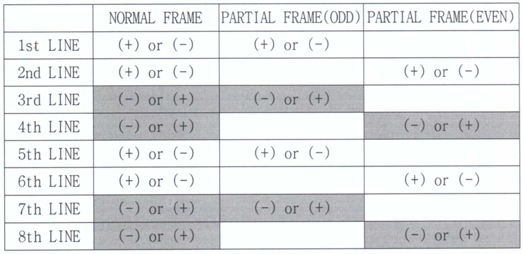
As shown in the following Table 1, when the inversion signal REV has the phase of the 1 + 2 dot inversion method in the normal frame, the inversion signal REV has the phase of the one-dot inversion method in the partial frame .
<Table 1>

Referring to Table 1 and FIG. 7A, in the normal frame, the
Referring to Table 1 and FIG. 7B, in the partial frame for processing odd-numbered data, the
On the other hand, referring to <Table 1> and FIG. 7C, in the partial frame processing the even-numbered data, on the
8A, 8B and 8C are conceptual diagrams illustrating a driving method of a display panel according to another embodiment of the present invention.
As shown in the following Table 2, when the inversion signal REV has a phase of the one-dot inversion method in the normal frame, the inversion signal REV is a positive (+) high level or negative (-) level of the column inversion method that maintains the low level.
<Table 2>

Referring to Table 2 and FIG. 8A, in the normal frame, the
Referring to Table 2 and FIG. 8B, in the partial frame processing the odd-numbered data, the
Referring to Table 2 and FIG. 8C, in the partial frame processing the even-numbered data, the
FIGS. 9A, 9B, and 9C are conceptual diagrams illustrating a driving method of a display panel according to another embodiment of the present invention.
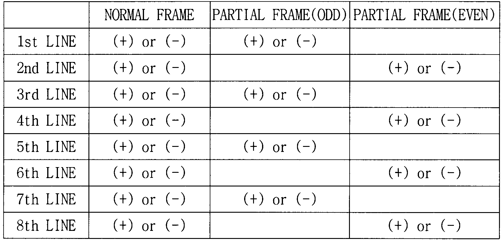
As shown in the following Table 3, when the inversion signal REV has the phase of the 2-dot inversion method in the normal frame, the inversion signal REV can have the phase of the 1-dot inversion method in the partial frame .
<Table 3>
Referring to Table 3 and FIG. 9A, in the normal frame, the
Referring to Table 3 and FIG. 9B, in the partial frame for processing odd-numbered data, the
Referring to Table 3 and FIG. 9C, in the partial frame processing the even-numbered data, the
10A, 10B, and 10C are conceptual diagrams illustrating a driving method of a display panel according to another embodiment of the present invention.
As summarized in Table 4, when the inversion signal REV has the phase of the column inversion scheme in the normal frame, the inversion signal REV may have the phase of the column inversion scheme as well as the partial inversion .
<Table 4>
Referring to Table 4 and FIG. 10A, in the normal frame, the
Referring to Table 4 and FIG. 10B, in the partial frame for processing the odd-numbered data, the
On the other hand, referring to Table 4 and FIG. 10C, in the partial frame processing the even-numbered data, in the
According to embodiments of the present invention, in the three-dimensional image mode, the inversion signal REV controls the polarity of the data voltage charged in the normal frame to be the same as the polarity of the data voltage charged in the partial frame. Accordingly, it is possible to improve the display quality of the three-dimensional image by eliminating flicker and horizontal line defect due to visual difference between the image displayed in the normal frame and the image displayed in the partial frame.
It will be understood by those skilled in the art that various changes in form and details may be made therein without departing from the spirit and scope of the invention as defined in the appended claims. It will be possible.
100: display panel 230: data driver
250: gate driver 270: timing controller
231: shift register 232: latch
233: Digital to Analog Converter 234: Output Buffer
251: first subgate circuit 252: second subgate circuit
Claims (20)
The data voltage of the first usage partial line having the same polarity as the data voltage of the first usage partial line output to the display panel in the first normal frame is displayed in the first partial frame shorter than the first normal frame, Outputting to a panel;
Outputting a data voltage of a second usage data frame to the display panel in a second normal frame having the same interval as the first normal frame;
A data voltage of the second usage partial line having the same polarity as the data voltage of the second usage partial line output to the display panel in the second normal frame in the second partial frame having the same section as the first partial frame, To the display panel; And
And controlling the polarity of the data voltage and generating an inverted signal whose phase is inverted with the period of the first normal frame, the first partial frame, the second normal frame and the second partial frame,
Wherein the inverted signal has the same phase in the first normal frame and the second normal frame, and has the same phase in the first partial circuit and the second partial frame, and the partial line is an odd- And a driving method of the display panel.
In the first normal frame and the second normal frame have a phase corresponding to the 1 + 2 dot inversion method, the first partial circuit and the second partial frame have a phase corresponding to the one-dot inversion method To the display panel.
Wherein when the first normal frame and the second normal frame have a phase corresponding to the one-dot inversion method, the first partial frame and the second partial frame have a phase corresponding to the column inversion method A method of driving a panel.
Wherein when the first normal frame and the second normal frame have a phase corresponding to the two dot inversion method, the first partial frame and the second partial frame have a phase corresponding to the one-dot inversion method A method of driving a display panel.
Wherein when the first normal frame and the second normal frame have a phase corresponding to the column inversion method, the first partial frame and the second partial frame have a phase corresponding to the column inversion method. .
Outputting a data voltage of a first use data frame to a data line of the display panel in a first normal frame and outputting a data voltage of a first data frame to a data line of the display panel in a first partial frame shorter than the first normal frame, In the second normal frame having the same interval as that of the first normal frame, the data voltage of the first usage partial line having the same polarity as the data voltage of the first use partial line is outputted to the data line of the display panel, Outputting the data voltage of the data frame for the second eye to the data line of the display panel and outputting the data voltage of the second useful portion outputted to the display panel in the second normal frame within the second partial frame having the same interval as the first partial frame The data voltage of the second usage partial line having the same polarity as the data voltage of the line, A data driver to output the line; And
And generating an inverted signal whose phase is inverted with the period of the first normal frame, the first partial frame, the second normal frame and the second partial frame, and having the same phase in the first normal frame and the second normal frame, And a timing controller for generating the inverted signal having the same phase in the first partial and the second partial,
Wherein the data driver controls the polarity of the data voltage based on the inverted signal, and the partial line is an odd-numbered or an even-numbered line.
The gate driver
A first sub-gate circuit for outputting an odd gate signal to odd-numbered gate lines; And
And a second sub-gate circuit for outputting even-numbered gate signals to the even-numbered gate lines.
And provides a vertical start signal to the gate driver at the beginning of each of the first normal frame, the first partial frame, the second normal frame, and the second partial frame.
A first sub-gate circuit for providing a first clock signal and a second clock signal inverted in phase with the first clock signal,
And provides a third clock signal to the second sub-gate circuit and a fourth clock signal that is inverted in phase with the third clock signal.
Providing the first and second clock signals to the first subgate circuit, or
And provides the third and fourth clock signals to the second sub-gate circuit.
Priority Applications (5)
| Application Number | Priority Date | Filing Date | Title |
|---|---|---|---|
| KR1020110046752A KR101818567B1 (en) | 2011-05-18 | 2011-05-18 | Method of driving display panel and display apparatus performing the method |
| US13/242,274 US9113158B2 (en) | 2011-05-18 | 2011-09-23 | Method of driving display panel and display apparatus for performing the method |
| EP11191441.2A EP2525583A3 (en) | 2011-05-18 | 2011-11-30 | Method of driving display panel and display apparatus for performing the method |
| CN201210008250.0A CN102789756B (en) | 2011-05-18 | 2012-01-09 | Drive the method for display floater and perform the display device of the method |
| JP2012003536A JP5964057B2 (en) | 2011-05-18 | 2012-01-11 | Display device |
Applications Claiming Priority (1)
| Application Number | Priority Date | Filing Date | Title |
|---|---|---|---|
| KR1020110046752A KR101818567B1 (en) | 2011-05-18 | 2011-05-18 | Method of driving display panel and display apparatus performing the method |
Publications (2)
| Publication Number | Publication Date |
|---|---|
| KR20120128853A KR20120128853A (en) | 2012-11-28 |
| KR101818567B1 true KR101818567B1 (en) | 2018-02-22 |
Family
ID=45421847
Family Applications (1)
| Application Number | Title | Priority Date | Filing Date |
|---|---|---|---|
| KR1020110046752A KR101818567B1 (en) | 2011-05-18 | 2011-05-18 | Method of driving display panel and display apparatus performing the method |
Country Status (5)
| Country | Link |
|---|---|
| US (1) | US9113158B2 (en) |
| EP (1) | EP2525583A3 (en) |
| JP (1) | JP5964057B2 (en) |
| KR (1) | KR101818567B1 (en) |
| CN (1) | CN102789756B (en) |
Families Citing this family (5)
| Publication number | Priority date | Publication date | Assignee | Title |
|---|---|---|---|---|
| CN102629453B (en) | 2011-05-25 | 2014-04-30 | 京东方科技集团股份有限公司 | Method for driving liquid crystal display panel in polarity-reversal mode and apparatus thereof |
| KR102019764B1 (en) * | 2012-12-21 | 2019-09-09 | 엘지디스플레이 주식회사 | Liquid crystal display device and driving method thereof |
| CN103208265B (en) * | 2013-04-15 | 2015-08-19 | 合肥京东方光电科技有限公司 | Liquid crystal display device polarity reversal driving method, device and liquid crystal display device |
| KR20160024048A (en) | 2014-08-22 | 2016-03-04 | 삼성디스플레이 주식회사 | Display device |
| KR102335113B1 (en) * | 2014-12-22 | 2021-12-03 | 삼성디스플레이 주식회사 | Display device and driving method thereof |
Citations (1)
| Publication number | Priority date | Publication date | Assignee | Title |
|---|---|---|---|---|
| JP2011075746A (en) * | 2009-09-30 | 2011-04-14 | Sony Corp | Image display device, image display observation system, and image display method |
Family Cites Families (31)
| Publication number | Priority date | Publication date | Assignee | Title |
|---|---|---|---|---|
| JP3155996B2 (en) * | 1995-12-12 | 2001-04-16 | アルプス電気株式会社 | Color liquid crystal display |
| US20010052887A1 (en) | 2000-04-11 | 2001-12-20 | Yusuke Tsutsui | Method and circuit for driving display device |
| JP4218249B2 (en) * | 2002-03-07 | 2009-02-04 | 株式会社日立製作所 | Display device |
| JP4095518B2 (en) * | 2002-10-31 | 2008-06-04 | セイコーエプソン株式会社 | Electro-optical device and electronic apparatus |
| CN1567419A (en) * | 2003-06-20 | 2005-01-19 | 统宝光电股份有限公司 | Polarity reversal driving method and apparatus for liquid crystal display panel |
| WO2005024769A1 (en) | 2003-09-08 | 2005-03-17 | Koninklijke Philips Electronics, N.V. | Electrophoretic display activation with blanking frames |
| US7576814B2 (en) * | 2004-03-29 | 2009-08-18 | Lg. Display Co., Ltd. | Liquid crystal display device of in-plane switching mode, method of fabricating the same, and method of driving the same |
| KR101090247B1 (en) * | 2004-04-19 | 2011-12-06 | 삼성전자주식회사 | Apparatus and method of driving 4 color device display |
| JP4572095B2 (en) * | 2004-07-15 | 2010-10-27 | Nec液晶テクノロジー株式会社 | Liquid crystal display device, portable device, and driving method of liquid crystal display device |
| US7724228B2 (en) * | 2004-11-29 | 2010-05-25 | Lg Display Co., Ltd. | Liquid crystal display device and driving method thereof |
| US8836621B2 (en) * | 2004-12-15 | 2014-09-16 | Nlt Technologies, Ltd. | Liquid crystal display apparatus, driving method for same, and driving circuit for same |
| US8847861B2 (en) * | 2005-05-20 | 2014-09-30 | Semiconductor Energy Laboratory Co., Ltd. | Active matrix display device, method for driving the same, and electronic device |
| TWI287775B (en) * | 2005-05-30 | 2007-10-01 | Prime View Int Co Ltd | Method for driving liquid crystal display panel |
| TWI298862B (en) * | 2005-10-28 | 2008-07-11 | Novatek Microelectronics Corp | Driving method and data driving circuit of plane surface display |
| JP4883524B2 (en) * | 2006-03-31 | 2012-02-22 | Nltテクノロジー株式会社 | Liquid crystal display device, drive control circuit used for the liquid crystal display device, and drive method |
| KR101315376B1 (en) * | 2006-08-02 | 2013-10-08 | 삼성디스플레이 주식회사 | Driving device of display device and method of modifying image signals thereof |
| KR20080089992A (en) * | 2007-04-03 | 2008-10-08 | 삼성전자주식회사 | Display substrate and liquid crystal display comprising the same |
| KR100859694B1 (en) | 2007-04-12 | 2008-09-23 | 삼성에스디아이 주식회사 | 2d/3d liquid display device and the driving method thereof |
| KR101274702B1 (en) * | 2007-05-25 | 2013-06-12 | 엘지디스플레이 주식회사 | Liquid Crystal Display and Driving Method thereof |
| KR101330459B1 (en) * | 2007-12-29 | 2013-11-15 | 엘지디스플레이 주식회사 | Liquid Crystal Display |
| DE102009002987B4 (en) * | 2008-05-16 | 2018-11-08 | Seereal Technologies S.A. | Controllable device for phase modulation |
| KR101599848B1 (en) | 2008-11-18 | 2016-03-07 | 엘지전자 주식회사 | 3-dimensional display and method for driving the same |
| US8390553B2 (en) * | 2009-02-13 | 2013-03-05 | Apple Inc. | Advanced pixel design for optimized driving |
| US8319528B2 (en) * | 2009-03-26 | 2012-11-27 | Semiconductor Energy Laboratory Co., Ltd. | Semiconductor device having interconnected transistors and electronic device including semiconductor device |
| EP2234100B1 (en) * | 2009-03-26 | 2016-11-02 | Semiconductor Energy Laboratory Co., Ltd. | Liquid crystal display device |
| JP2010256420A (en) * | 2009-04-21 | 2010-11-11 | Sony Corp | Liquid crystal display and driving method therefor |
| JP2010266601A (en) * | 2009-05-13 | 2010-11-25 | Seiko Epson Corp | Photoelectric device and electronic equipment |
| JP5175977B2 (en) * | 2009-05-22 | 2013-04-03 | シャープ株式会社 | 3D display device |
| JP5629439B2 (en) * | 2009-08-26 | 2014-11-19 | 株式会社ジャパンディスプレイ | Liquid crystal display |
| TW201129078A (en) * | 2010-02-01 | 2011-08-16 | Chunghwa Picture Tubes Ltd | Stereoscopic image displaying method |
| TWI410914B (en) * | 2010-03-12 | 2013-10-01 | Acer Inc | Liquid crystal display and control method thereof |
-
2011
- 2011-05-18 KR KR1020110046752A patent/KR101818567B1/en active IP Right Grant
- 2011-09-23 US US13/242,274 patent/US9113158B2/en not_active Expired - Fee Related
- 2011-11-30 EP EP11191441.2A patent/EP2525583A3/en not_active Ceased
-
2012
- 2012-01-09 CN CN201210008250.0A patent/CN102789756B/en not_active Expired - Fee Related
- 2012-01-11 JP JP2012003536A patent/JP5964057B2/en not_active Expired - Fee Related
Patent Citations (1)
| Publication number | Priority date | Publication date | Assignee | Title |
|---|---|---|---|---|
| JP2011075746A (en) * | 2009-09-30 | 2011-04-14 | Sony Corp | Image display device, image display observation system, and image display method |
Also Published As
| Publication number | Publication date |
|---|---|
| EP2525583A2 (en) | 2012-11-21 |
| CN102789756B (en) | 2016-09-07 |
| US9113158B2 (en) | 2015-08-18 |
| JP5964057B2 (en) | 2016-08-03 |
| CN102789756A (en) | 2012-11-21 |
| JP2012242819A (en) | 2012-12-10 |
| US20120293495A1 (en) | 2012-11-22 |
| KR20120128853A (en) | 2012-11-28 |
| EP2525583A3 (en) | 2014-05-21 |
Similar Documents
| Publication | Publication Date | Title |
|---|---|---|
| KR101804890B1 (en) | Method of driving display panel and a display apparatus performing the method | |
| KR101477967B1 (en) | Method of driving display panel and display apparatus for performing the same | |
| KR101950204B1 (en) | Method of driving display panel and display apparatus for performing the same | |
| JP6081698B2 (en) | Display panel driving method and display device executing the same | |
| KR101738476B1 (en) | Method of driving display panel and display device performing the method | |
| KR101906402B1 (en) | Method of driving display panel and display apparatu7s for performing the same | |
| US10102811B2 (en) | Method of displaying three-dimensional image and display apparatus using the same | |
| KR101818567B1 (en) | Method of driving display panel and display apparatus performing the method | |
| KR20140003685A (en) | 3d image display device and driving method thereof | |
| KR101817939B1 (en) | Method of processing three-dimension image data and display apparatus performing the same | |
| US9088788B2 (en) | Method of displaying a three dimensional image and display apparatus for performing the method | |
| KR20120109720A (en) | Method of driving display panel and dispay apparatus performing the method | |
| CN104280968A (en) | Liquid crystal panel and pixel black insertion method during 3D display of liquid crystal panel | |
| KR101921963B1 (en) | Display apparatus and method of driving the same | |
| US20160063932A1 (en) | Overdrive method, circuit, and display device | |
| WO2016033831A1 (en) | Over drive method, circuit and display device | |
| US20150221263A1 (en) | Three-dimensional image display device and driving method thereof | |
| US20110216174A1 (en) | Method for displaying stereoscopic images |
Legal Events
| Date | Code | Title | Description |
|---|---|---|---|
| N231 | Notification of change of applicant | ||
| A201 | Request for examination | ||
| E902 | Notification of reason for refusal | ||
| E701 | Decision to grant or registration of patent right | ||
| GRNT | Written decision to grant |