US8253489B2 - Amplifier, transmitter, and method for compensating gain - Google Patents

Amplifier, transmitter, and method for compensating gain Download PDF

Info

Publication number
US8253489B2
US8253489B2 US12/756,295 US75629510A US8253489B2 US 8253489 B2 US8253489 B2 US 8253489B2 US 75629510 A US75629510 A US 75629510A US 8253489 B2 US8253489 B2 US 8253489B2
Authority
US
United States
Prior art keywords
gain compensation
voltage difference
gan
signal
gain
Prior art date
Legal status (The legal status is an assumption and is not a legal conclusion. Google has not performed a legal analysis and makes no representation as to the accuracy of the status listed.)
Expired - Fee Related
Application number
US12/756,295
Other versions
US20100289585A1 (en
Inventor
Fumihiro Tomisawa
Tatsuhiko Tajima
Current Assignee (The listed assignees may be inaccurate. Google has not performed a legal analysis and makes no representation or warranty as to the accuracy of the list.)
Fujitsu Ltd
Original Assignee
Fujitsu Ltd
Priority date (The priority date is an assumption and is not a legal conclusion. Google has not performed a legal analysis and makes no representation as to the accuracy of the date listed.)
Filing date
Publication date
Application filed by Fujitsu Ltd filed Critical Fujitsu Ltd
Assigned to FUJITSU LIMITED reassignment FUJITSU LIMITED ASSIGNMENT OF ASSIGNORS INTEREST (SEE DOCUMENT FOR DETAILS). Assignors: TAJIMA, TATSUHIKO, Tomisawa, Fumihiro
Publication of US20100289585A1 publication Critical patent/US20100289585A1/en
Application granted granted Critical
Publication of US8253489B2 publication Critical patent/US8253489B2/en
Expired - Fee Related legal-status Critical Current
Anticipated expiration legal-status Critical

Links

Images

Classifications

    • HELECTRICITY
    • H03ELECTRONIC CIRCUITRY
    • H03FAMPLIFIERS
    • H03F1/00Details of amplifiers with only discharge tubes, only semiconductor devices or only unspecified devices as amplifying elements
    • H03F1/30Modifications of amplifiers to reduce influence of variations of temperature or supply voltage or other physical parameters
    • H03F1/303Modifications of amplifiers to reduce influence of variations of temperature or supply voltage or other physical parameters using a switching device
    • H03F1/304Modifications of amplifiers to reduce influence of variations of temperature or supply voltage or other physical parameters using a switching device and using digital means
    • HELECTRICITY
    • H03ELECTRONIC CIRCUITRY
    • H03FAMPLIFIERS
    • H03F1/00Details of amplifiers with only discharge tubes, only semiconductor devices or only unspecified devices as amplifying elements
    • H03F1/30Modifications of amplifiers to reduce influence of variations of temperature or supply voltage or other physical parameters
    • H03F1/301Modifications of amplifiers to reduce influence of variations of temperature or supply voltage or other physical parameters in MOSFET amplifiers

Definitions

  • the embodiment discussed herein is directed to an apparatus such as an amplifier for amplifying a signal.
  • amplifiers using a device such as a FET (Field Effect Transistor) circuit element are employed in wireless base stations for sending and receiving communication signals.
  • a device such as LDMOS-FET and GaAs-FET have been employed.
  • amplifiers using a highly efficient GaN-HEMT GaN-HEMT (Gallium Nitride High Electron Mobility Transistor) capable of operating at lower power than the previous amplifiers are becoming mainstream.
  • GaN-HEMT GaN-HEMT
  • an amplifier using a GaN-HEMT device is denoted as a high power amplifier.
  • the aforementioned high power amplifier causes an Idq drift when the amplifier controls the output level of the GaN-HEMT device from high power to low power.
  • an idle current (Idq) becomes equal to or lower than a prescribed value.
  • Such an Idq drift causes the gain of the GaN-HEMT device to fluctuate by a large degree.
  • an amplifier includes a voltage detector that detects current flowing to a drain terminal of a transistor which amplifies a signal using GaN as a voltage difference by means of voltage conversion, a compensation decision unit that decides whether or not to perform gain compensation based on the voltage difference detected by the voltage detector, and a gain compensation unit that performs the gain compensation according to the voltage difference when the compensation decision unit decides to perform the gain compensation.
  • FIG. 1 is a graph illustrating a relation between the idle current Idq and the temperature T of GaN-HEMT
  • FIG. 2 is a graph illustrating a relation between the idle current Idq and the gain of GaN-HEMT
  • FIG. 3 is a graph illustrating a relation between a drain current Idq input in a GaN-HEMT device and the gain
  • FIG. 4 is a graph for illustrating an outline of a transmitter according to an embodiment of the present invention.
  • FIG. 5 is a diagram illustrating a configuration of the transmitter according to the embodiment of the present invention.
  • FIG. 6 is a diagram illustrating a schematic configuration of a high power amplifier according to the embodiment of the present invention.
  • FIG. 7 is a diagram illustrating a detailed configuration of the high power amplifier according to the embodiment of the present invention.
  • FIG. 8 is a flowchart illustrating a processing procedure of the high power amplifier according to the embodiment of the present invention.
  • the Idq drift is a phenomenon that an idle current (Idq) at the initial setting of a GaN-HEMT device, for example, in a high power amplifier fluctuates under various conditions.
  • the idle current corresponds to a drain current in the condition where a signal is not applied to the GaN-HEMT device.
  • Idq drift occurs prominently when the GaN-HEMT device is at a low temperature, and does not occur when the GaN-HEMT device is at a high temperature.
  • FIG. 1 is a graph illustrating a relation between idle current Idq and temperature T of GaN-HEMT.
  • setting value of the normal idle current of a GaN-HEMT device is 0.4 A.
  • the idle current lowers significantly with a decrease of the temperature of the GaN-HEMT device. For example, when the temperature of the GaN-HEMT device is as low as ⁇ 20° C., the idle current of the GaN-HEMT device becomes 0.05 A.
  • variation amount of the idle current with an increase of the temperature of the GaN-HEMT device is small.
  • FIG. 2 is a graph illustrating a relation between the idle current Idq and the gain of GaN-HEMT.
  • the normal gain of the GaN-HEMT device is about 23 dB.
  • the gain of the GaN-HEMT device decreases significantly when the output level is lowered while the idle current is low after the idle current decreases because of the effect of temperature drop. For example, if the output level is lowered when the idle current is 0.05 A, the gain of the GaN-HEMT device drops from the normal 23 dB to 20 dB.
  • a large gain fluctuation does not occur at high temperature, because the variation amount of the idle current along with an increase of the temperature of the GaN-HEMT device is small.
  • FIG. 3 is a graph illustrating a relation between the drain current Idq input to the GaN-HEMT device and the gain. As illustrated in FIG. 3 , the normal gain of the GaN-HEMT device is about 23 dB. When the drain current input to the drain terminal of the GaN-HEMT device falls, the gain drops.
  • the gain of the GaN-HEMT device drops because of the Idq drift when the value of the drain current falls below the prescribed value. Because the idle current represents a current in the situation when the current is not input to the GaN-HEMT device, it is not possible to perform gain compensation by monitoring the idle current itself.
  • the drain current can be monitored even when the current is input to the GaN-HEMT device. Therefore, if the gain compensation is performed dynamically based on the drain current, a large fluctuation in the gain of the GaN-HEMT device due to the Idq drift can be prevented.
  • FIG. 4 is a diagram for illustrating an outline of a transmitter according to the embodiment of the present invention.
  • the transmitter according to the embodiment of the present invention monitors the drain current input to the drain terminal of the GaN-HEMT device and decides whether the value of the drain current becomes lower than a prescribed value or not. If the value of the drain current becomes lower than the prescribed value, the transmitter performs gain compensation dependent on the drain current.
  • the transmitter performs gain compensation so that the gain returns to 23 dB.
  • the transmitter according to the embodiment of the present invention can prevent the large fluctuation of the gain of the GaN-HEMT device caused by the Idq drift by performing gain compensation based on the drain current.
  • FIG. 5 is a diagram illustrating a configuration of the transmitter according to the embodiment of the present invention.
  • a transmitter 100 includes a distortion compensation unit 110 , a D/A converter 120 , a QMOD 130 , a high power amplifier 140 , a DUP 150 , and an A/D converter 160 .
  • the distortion compensation unit 110 is a processing unit that includes an APD or an FPGA.
  • the distortion compensation unit 110 acquires information of a signal fed back from the high power amplifier 140 , and compensates the distortion of the signal based on the acquired information.
  • the D/A converter 120 is a processing unit for acquiring a digital signal from the distortion compensation unit 110 , converting the digital signal into an analog signal, and outputting the converted analog signal to the QMOD 130 .
  • the QMOD (quadrature modulator) 130 is a processing unit for executing quadrature modulation on the acquired signal when it acquires a signal from the D/A converter 120 .
  • the QMOD 130 outputs a quadrature-modulated signal to the high power amplifier 140 .
  • the high power amplifier 140 acquires a signal from the QMOD 130 and amplifies the signal using the GaN-HEMT device.
  • the high power amplifier 140 divides the amplified signal using a coupler and outputs the amplified signal to the DUP 150 and the A/D converter 160 .
  • the high power amplifier 140 performs gain compensation based on the drain current of the GaN-HEMT device.
  • the DUP (Duplexer) 150 is an antenna-shared device and reduces the transmission loss of a signal output from the high power amplifier 140 or a signal received from an antenna.
  • the A/D converter 160 is a processing unit for acquiring an analog signal from the high power amplifier 140 , converting the acquired analog signal into a digital signal, and outputting the digital signal after conversion to the distortion compensation unit 110 .
  • FIG. 6 is a diagram illustrating the schematic configuration of the high power amplifier 140 according to the embodiment of the present invention.
  • the high power amplifier 140 includes a GaN-HEMT device 141 , a voltage detector 142 , a gain compensation decision circuit 143 , a control circuit 144 , and a gain compensation circuit 145 .
  • the GaN-HEMT device 141 connected to Vg (gate bias) and Vd (drain bias) is a circuit to amplify a signal that the QMOD 130 illustrated in FIG. 5 outputs.
  • the voltage detector 142 is a processing unit for detecting a current flowing to the drain terminal of the GaN-HEMT device 141 as a potential difference (voltage) by means of voltage conversion.
  • the voltage detector 142 outputs the voltage value as a detection result to the gain compensation decision circuit 143 and the control circuit 144 .
  • the gain compensation decision circuit 143 acquires the voltage value from the voltage detector 142 and decides whether or not to perform gain compensation based on the acquired voltage value. Specifically, the gain compensation decision circuit 143 decides to perform gain compensation if the voltage value is less than a prescribed value, and decides not to perform gain compensation if the voltage value is equal to or more than the prescribed value. The gain compensation decision circuit 143 outputs the decision result to the control circuit 144 .
  • the control circuit 144 acquires the decision result from the gain compensation decision circuit 143 and acquires the voltage value from the voltage detector 142 .
  • the control circuit 144 further outputs the voltage value based on the decision result to the gain compensation circuit 145 . Specifically, if the control circuit 144 acquires the decision result indicating gain compensation, the control circuit 144 outputs the voltage value to the gain compensation circuit 145 . On the other hand, if the control circuit 144 acquires the decision result indicating no gain compensation, the control circuit 144 does not output the voltage value to the gain compensation circuit 145 .
  • the gain compensation circuit 145 is a circuit for performing gain compensation on acquiring the voltage value from the control circuit 144 , according to the acquired voltage value. For example, the gain compensation circuit 145 performs gain compensation by adjusting an attenuation amount of a signal, which is sent through a signal line, according to the voltage value.
  • FIG. 7 is a diagram illustrating the detailed configuration of the high power amplifier 140 according to the embodiment of the present invention.
  • the high power amplifier 140 includes the GaN-HEMT device 141 , the voltage detector 142 , the gain compensation decision circuit 143 , the control circuit 144 , and the gain compensation circuit 145 .
  • the signal line for sending a signal includes DC cut capacitors 10 for cutting the DC component of the signal.
  • the GaN-HEMT device 141 connected to the Vg (gate bias) and the Vd (drain bias) is a circuit for amplifying a signal that the QMOD 130 illustrated in FIG. 5 outputs.
  • a line connecting the Vg and the GaN-HEMT device 141 is connected to a plurality of capacitors 11 .
  • a line connecting the Vd and the GaN-HEMT device 141 is connected to a plurality of capacitors 11 and a resistor 141 a.
  • the voltage detector 142 includes a differential amplifier circuit 142 a including a plurality of resistors R 1 to R 4 .
  • the voltage detector 142 amplifies a voltage difference between a voltage V 1 applied from a line connected to one terminal of the resistor 141 a and a voltage V 2 applied from a line connected to the other terminal of the resistor 141 a.
  • the voltage detector 142 outputs the amplified voltage difference V out to the gain compensation decision circuit 143 and the control circuit 144 .
  • the gain compensation decision circuit 143 includes a comparator 143 a and resistors R 5 and R 6 .
  • the gain compensation decision circuit 143 decides whether or not the value of the voltage difference V out is larger than a voltage applied from a line connecting the resistors R 5 and R 6 . If the value of the voltage difference V out is smaller than the voltage applied from the line connecting the resistors R 5 and R 6 , the gain compensation decision circuit 143 outputs an H signal to the control circuit 144 . On the other hand, if the value of the voltage difference V out is larger than the voltage applied from the line connecting the resistors R 5 and R 6 , the gain compensation decision circuit 143 outputs an L signal to the control circuit 144 .
  • the control circuit 144 includes a transistor switch 144 a.
  • the control circuit 144 outputs the voltage difference V out to the gain compensation circuit 145 on acquiring the H signal from the gain compensation decision circuit 143 .
  • the control circuit 144 does not output the voltage difference V out to the gain compensation circuit 145 on acquiring the L signal from the gain compensation decision circuit 143 .
  • the gain compensation circuit 145 includes a V-ATT (attenuator) 145 a.
  • the gain compensation circuit 145 performs gain compensation by giving an attenuation amount corresponding to the voltage difference V out to the signal when the gain compensation circuit 145 receives the voltage difference V out from the control circuit 144 . It is assumed that a voltage gradient illustrating the relation between the voltage difference V out and the attenuation amount is adjusted based on a property of the gain compensation circuit 145 and a property of a differential amplifier circuit 142 a.
  • FIG. 8 is a flowchart illustrating the processing procedure of the high power amplifier 140 according to the embodiment of the present invention.
  • the voltage detector 142 outputs the voltage difference between both ends of the resistor 141 a connected to the Vd (Step S 101 ).
  • the gain compensation decision circuit 143 decides whether or not to perform the gain compensation based on the voltage difference (Step S 102 ). If the gain compensation decision circuit 143 decides not to perform the gain compensation (Step S 103 , No), the process proceeds to Step S 101 . On the other hand, if the gain compensation decision circuit 143 decides to perform the gain compensation (Step S 103 , Yes), the gain compensation circuit 145 controls the attenuation amount according to the voltage difference (Step S 104 ), and the process proceeds to Step S 101 .
  • the high power amplifier 140 outputs the voltage difference based on the voltage between both ends of the resistor 141 a , which is connected to the drain bias connected to the GaN-HEMT device. Then, whether to perform the gain compensation is decided based on the voltage difference.
  • the high power amplifier 140 specifies the attenuation amount based on the voltage difference when performing the gain compensation and performs the gain compensation by giving the specified attenuation amount to the signal line. Therefore, a large gain fluctuation caused by the Idq drift can be efficiently compensated.
  • whether to perform the gain compensation is decided based on a voltage difference, and the specified attenuation amount corresponds to the voltage difference, by way of example.
  • the drain current may be used in place of the voltage difference.

Landscapes

  • Engineering & Computer Science (AREA)
  • Power Engineering (AREA)
  • Amplifiers (AREA)
  • Control Of Amplification And Gain Control (AREA)
  • Transmitters (AREA)

Abstract

An amplifier includes a voltage detector that detects current flowing to a drain terminal of a transistor which amplifies a signal using GaN as a voltage difference by means of voltage conversion, a compensation decision unit that decides whether or not to perform gain compensation based on the voltage difference detected by the voltage detector, and a gain compensation unit that performs the gain compensation according to the voltage difference when the compensation decision unit decides to perform the gain compensation.

Description

CROSS-REFERENCE TO RELATED APPLICATION
This application is based upon and claims the benefit of priority of the prior Japanese Patent Application No. 2009-120189, filed on May 18, 2009, the entire contents of which are incorporated herein by reference.
FIELD
The embodiment discussed herein is directed to an apparatus such as an amplifier for amplifying a signal.
BACKGROUND
In recent years, amplifiers using a device such as a FET (Field Effect Transistor) circuit element are employed in wireless base stations for sending and receiving communication signals. Previously, amplifiers using a device such as LDMOS-FET and GaAs-FET have been employed. Recently, however, amplifiers using a highly efficient GaN-HEMT (Gallium Nitride High Electron Mobility Transistor) capable of operating at lower power than the previous amplifiers are becoming mainstream. In the explanation hereinafter, an amplifier using a GaN-HEMT device is denoted as a high power amplifier.
However, the aforementioned high power amplifier causes an Idq drift when the amplifier controls the output level of the GaN-HEMT device from high power to low power. In the Idq drift, an idle current (Idq) becomes equal to or lower than a prescribed value. Such an Idq drift causes the gain of the GaN-HEMT device to fluctuate by a large degree.
Although a small gain fluctuation in a general amplifier is compensated in an existing apparatus, a large gain fluctuation caused by the Idq drift is not compensated in the existing apparatus. Therefore, when a large gain fluctuation occurs by the Idq drift, control for compensating the fluctuation becomes unstable. As a result, it takes time until the compensation of the gain fluctuation is completed (as examples of conventional technology, see Japanese Laid-open Patent Publication No. 08-32357, and Japanese Laid-open Patent Publication No. 10-294628).
SUMMARY
According to an aspect of an embodiment of the invention, an amplifier includes a voltage detector that detects current flowing to a drain terminal of a transistor which amplifies a signal using GaN as a voltage difference by means of voltage conversion, a compensation decision unit that decides whether or not to perform gain compensation based on the voltage difference detected by the voltage detector, and a gain compensation unit that performs the gain compensation according to the voltage difference when the compensation decision unit decides to perform the gain compensation.
The object and advantages of the embodiment will be realized and attained by means of the elements and combinations particularly pointed out in the claims.
It is to be understood that both the foregoing general description and the following detailed description are exemplary and explanatory and are not restrictive of the embodiment, as claimed.
BRIEF DESCRIPTION OF DRAWINGS
FIG. 1 is a graph illustrating a relation between the idle current Idq and the temperature T of GaN-HEMT;
FIG. 2 is a graph illustrating a relation between the idle current Idq and the gain of GaN-HEMT;
FIG. 3 is a graph illustrating a relation between a drain current Idq input in a GaN-HEMT device and the gain;
FIG. 4 is a graph for illustrating an outline of a transmitter according to an embodiment of the present invention;
FIG. 5 is a diagram illustrating a configuration of the transmitter according to the embodiment of the present invention;
FIG. 6 is a diagram illustrating a schematic configuration of a high power amplifier according to the embodiment of the present invention;
FIG. 7 is a diagram illustrating a detailed configuration of the high power amplifier according to the embodiment of the present invention; and
FIG. 8 is a flowchart illustrating a processing procedure of the high power amplifier according to the embodiment of the present invention.
DESCRIPTION OF EMBODIMENT(S)
Preferred embodiments of the present invention will be explained with reference to accompanying drawings. It should be noted that the present invention is not limited by this embodiment.
First, before explaining the embodiment of the present invention, the Idq drift of GaN-HEMT is explained. The Idq drift is a phenomenon that an idle current (Idq) at the initial setting of a GaN-HEMT device, for example, in a high power amplifier fluctuates under various conditions. The idle current corresponds to a drain current in the condition where a signal is not applied to the GaN-HEMT device.
One condition for causing the Idq drift is that the output level of the high power amplifier is decreased, for example, from a rated output level to a level 20 dB lower than a dynamic range predetermined by the specifications of the apparatus. Such Idq drift occurs prominently when the GaN-HEMT device is at a low temperature, and does not occur when the GaN-HEMT device is at a high temperature.
FIG. 1 is a graph illustrating a relation between idle current Idq and temperature T of GaN-HEMT. As illustrated in FIG. 1, setting value of the normal idle current of a GaN-HEMT device is 0.4 A. The idle current lowers significantly with a decrease of the temperature of the GaN-HEMT device. For example, when the temperature of the GaN-HEMT device is as low as −20° C., the idle current of the GaN-HEMT device becomes 0.05 A. On the other hand, variation amount of the idle current with an increase of the temperature of the GaN-HEMT device is small.
FIG. 2 is a graph illustrating a relation between the idle current Idq and the gain of GaN-HEMT. As illustrated in FIG. 2, the normal gain of the GaN-HEMT device is about 23 dB. However, the gain of the GaN-HEMT device decreases significantly when the output level is lowered while the idle current is low after the idle current decreases because of the effect of temperature drop. For example, if the output level is lowered when the idle current is 0.05 A, the gain of the GaN-HEMT device drops from the normal 23 dB to 20 dB. On the other hand, a large gain fluctuation does not occur at high temperature, because the variation amount of the idle current along with an increase of the temperature of the GaN-HEMT device is small.
Next, a relation between the gain and the drain current input to the GaN-HEMT device when the Idq drift occurs is explained. FIG. 3 is a graph illustrating a relation between the drain current Idq input to the GaN-HEMT device and the gain. As illustrated in FIG. 3, the normal gain of the GaN-HEMT device is about 23 dB. When the drain current input to the drain terminal of the GaN-HEMT device falls, the gain drops.
Here, when comparing FIG. 2 and FIG. 3, it is found that the relation between the idle current and the gain correlates with the relation between the drain current and the gain. Therefore, it is considered that the gain of the GaN-HEMT device drops because of the Idq drift when the value of the drain current falls below the prescribed value. Because the idle current represents a current in the situation when the current is not input to the GaN-HEMT device, it is not possible to perform gain compensation by monitoring the idle current itself.
On the other hand, the drain current can be monitored even when the current is input to the GaN-HEMT device. Therefore, if the gain compensation is performed dynamically based on the drain current, a large fluctuation in the gain of the GaN-HEMT device due to the Idq drift can be prevented.
Next, an outline of a transmitter according to the embodiment of the present invention is explained. FIG. 4 is a diagram for illustrating an outline of a transmitter according to the embodiment of the present invention. As illustrated in FIG. 4, the transmitter according to the embodiment of the present invention monitors the drain current input to the drain terminal of the GaN-HEMT device and decides whether the value of the drain current becomes lower than a prescribed value or not. If the value of the drain current becomes lower than the prescribed value, the transmitter performs gain compensation dependent on the drain current.
For example, in FIG. 4, when the drain current is 0.1 A, the gain of the GaN-HEMT device drops from 23 dB to 20 dB. Hence, when the drain current is found to be 0.1 A as a result of monitoring of the drain current, the transmitter performs gain compensation so that the gain returns to 23 dB.
As described above, the transmitter according to the embodiment of the present invention can prevent the large fluctuation of the gain of the GaN-HEMT device caused by the Idq drift by performing gain compensation based on the drain current.
Next, a configuration of the transmitter according to the embodiment of the present invention is illustrated. FIG. 5 is a diagram illustrating a configuration of the transmitter according to the embodiment of the present invention. As illustrated in FIG. 5, a transmitter 100 includes a distortion compensation unit 110, a D/A converter 120, a QMOD 130, a high power amplifier 140, a DUP 150, and an A/D converter 160.
Among these components, the distortion compensation unit 110 is a processing unit that includes an APD or an FPGA. The distortion compensation unit 110 acquires information of a signal fed back from the high power amplifier 140, and compensates the distortion of the signal based on the acquired information.
The D/A converter 120 is a processing unit for acquiring a digital signal from the distortion compensation unit 110, converting the digital signal into an analog signal, and outputting the converted analog signal to the QMOD 130. The QMOD (quadrature modulator) 130 is a processing unit for executing quadrature modulation on the acquired signal when it acquires a signal from the D/A converter 120. The QMOD 130 outputs a quadrature-modulated signal to the high power amplifier 140.
The high power amplifier 140 acquires a signal from the QMOD 130 and amplifies the signal using the GaN-HEMT device. The high power amplifier 140 divides the amplified signal using a coupler and outputs the amplified signal to the DUP 150 and the A/D converter 160. In addition, as illustrated in FIG. 4, the high power amplifier 140 performs gain compensation based on the drain current of the GaN-HEMT device.
The DUP (Duplexer) 150 is an antenna-shared device and reduces the transmission loss of a signal output from the high power amplifier 140 or a signal received from an antenna. The A/D converter 160 is a processing unit for acquiring an analog signal from the high power amplifier 140, converting the acquired analog signal into a digital signal, and outputting the digital signal after conversion to the distortion compensation unit 110.
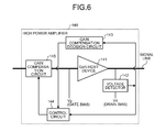
Next, a schematic configuration of the high power amplifier 140 illustrated in FIG. 5 is explained. FIG. 6 is a diagram illustrating the schematic configuration of the high power amplifier 140 according to the embodiment of the present invention. As illustrated in FIG. 6, the high power amplifier 140 includes a GaN-HEMT device 141, a voltage detector 142, a gain compensation decision circuit 143, a control circuit 144, and a gain compensation circuit 145.
Among these components, the GaN-HEMT device 141 connected to Vg (gate bias) and Vd (drain bias) is a circuit to amplify a signal that the QMOD 130 illustrated in FIG. 5 outputs. The voltage detector 142 is a processing unit for detecting a current flowing to the drain terminal of the GaN-HEMT device 141 as a potential difference (voltage) by means of voltage conversion. The voltage detector 142 outputs the voltage value as a detection result to the gain compensation decision circuit 143 and the control circuit 144.
The gain compensation decision circuit 143 acquires the voltage value from the voltage detector 142 and decides whether or not to perform gain compensation based on the acquired voltage value. Specifically, the gain compensation decision circuit 143 decides to perform gain compensation if the voltage value is less than a prescribed value, and decides not to perform gain compensation if the voltage value is equal to or more than the prescribed value. The gain compensation decision circuit 143 outputs the decision result to the control circuit 144.
The control circuit 144 acquires the decision result from the gain compensation decision circuit 143 and acquires the voltage value from the voltage detector 142. The control circuit 144 further outputs the voltage value based on the decision result to the gain compensation circuit 145. Specifically, if the control circuit 144 acquires the decision result indicating gain compensation, the control circuit 144 outputs the voltage value to the gain compensation circuit 145. On the other hand, if the control circuit 144 acquires the decision result indicating no gain compensation, the control circuit 144 does not output the voltage value to the gain compensation circuit 145.
The gain compensation circuit 145 is a circuit for performing gain compensation on acquiring the voltage value from the control circuit 144, according to the acquired voltage value. For example, the gain compensation circuit 145 performs gain compensation by adjusting an attenuation amount of a signal, which is sent through a signal line, according to the voltage value.
Next, the configuration of the high power amplifier 140 illustrated in FIG. 6 is explained more specifically. FIG. 7 is a diagram illustrating the detailed configuration of the high power amplifier 140 according to the embodiment of the present invention. As illustrated in FIG. 7, the high power amplifier 140 includes the GaN-HEMT device 141, the voltage detector 142, the gain compensation decision circuit 143, the control circuit 144, and the gain compensation circuit 145. In addition, the signal line for sending a signal includes DC cut capacitors 10 for cutting the DC component of the signal.
The GaN-HEMT device 141 connected to the Vg (gate bias) and the Vd (drain bias) is a circuit for amplifying a signal that the QMOD 130 illustrated in FIG. 5 outputs. In addition, a line connecting the Vg and the GaN-HEMT device 141 is connected to a plurality of capacitors 11. Moreover, a line connecting the Vd and the GaN-HEMT device 141 is connected to a plurality of capacitors 11 and a resistor 141 a.
The voltage detector 142 includes a differential amplifier circuit 142 a including a plurality of resistors R1 to R4. The voltage detector 142 amplifies a voltage difference between a voltage V1 applied from a line connected to one terminal of the resistor 141 a and a voltage V2 applied from a line connected to the other terminal of the resistor 141 a. The voltage detector 142 outputs the amplified voltage difference Vout to the gain compensation decision circuit 143 and the control circuit 144.
The gain compensation decision circuit 143 includes a comparator 143 a and resistors R5 and R6. The gain compensation decision circuit 143 decides whether or not the value of the voltage difference Vout is larger than a voltage applied from a line connecting the resistors R5 and R6. If the value of the voltage difference Vout is smaller than the voltage applied from the line connecting the resistors R5 and R6, the gain compensation decision circuit 143 outputs an H signal to the control circuit 144. On the other hand, if the value of the voltage difference Vout is larger than the voltage applied from the line connecting the resistors R5 and R6, the gain compensation decision circuit 143 outputs an L signal to the control circuit 144.
The control circuit 144 includes a transistor switch 144 a. The control circuit 144 outputs the voltage difference Vout to the gain compensation circuit 145 on acquiring the H signal from the gain compensation decision circuit 143. On the other hand, the control circuit 144 does not output the voltage difference Vout to the gain compensation circuit 145 on acquiring the L signal from the gain compensation decision circuit 143.
The gain compensation circuit 145 includes a V-ATT (attenuator) 145 a. The gain compensation circuit 145 performs gain compensation by giving an attenuation amount corresponding to the voltage difference Vout to the signal when the gain compensation circuit 145 receives the voltage difference Vout from the control circuit 144. It is assumed that a voltage gradient illustrating the relation between the voltage difference Vout and the attenuation amount is adjusted based on a property of the gain compensation circuit 145 and a property of a differential amplifier circuit 142 a.
Next, a processing procedure of the high power amplifier 140 of the embodiment of the present invention is explained. FIG. 8 is a flowchart illustrating the processing procedure of the high power amplifier 140 according to the embodiment of the present invention. As illustrated in FIG. 8, in the high power amplifier 140, the voltage detector 142 outputs the voltage difference between both ends of the resistor 141 a connected to the Vd (Step S101).
The gain compensation decision circuit 143 decides whether or not to perform the gain compensation based on the voltage difference (Step S102). If the gain compensation decision circuit 143 decides not to perform the gain compensation (Step S103, No), the process proceeds to Step S101. On the other hand, if the gain compensation decision circuit 143 decides to perform the gain compensation (Step S103, Yes), the gain compensation circuit 145 controls the attenuation amount according to the voltage difference (Step S104), and the process proceeds to Step S101.
As described above, in the transmitter 100 according to the embodiment of the present invention, the high power amplifier 140 outputs the voltage difference based on the voltage between both ends of the resistor 141 a, which is connected to the drain bias connected to the GaN-HEMT device. Then, whether to perform the gain compensation is decided based on the voltage difference. The high power amplifier 140 specifies the attenuation amount based on the voltage difference when performing the gain compensation and performs the gain compensation by giving the specified attenuation amount to the signal line. Therefore, a large gain fluctuation caused by the Idq drift can be efficiently compensated.
In the embodiment of the present invention, whether to perform the gain compensation is decided based on a voltage difference, and the specified attenuation amount corresponds to the voltage difference, by way of example. Alternatively, however, the drain current may be used in place of the voltage difference.
In the meantime, among the processings explained in the embodiment of the present invention, all or part of the processings can be done manually; or all or part of the processings explained to be done manually can also be done automatically using heretofore known methods. In addition, information including the processing procedures, control procedures, specific names, and various data and parameters illustrated in the above description and the drawings can be changed arbitrarily if not otherwise specified.
According to the amplifier of the embodiment, a large gain fluctuation caused by the Idq drift can be efficiently compensated.
All examples and conditional language recited herein are intended for pedagogical purposes to aid the reader in understanding the invention and the concepts contributed by the inventor to furthering the art, and are to be construed as being without limitation to such specifically recited examples and conditions, nor does the organization of such examples in the specification relate to a showing of the superiority and inferiority of the invention. Although the embodiment of the present invention has been described in detail, it should be understood that the various changes, substitutions, and alterations could be made hereto without departing from the spirit and scope of the invention.

Claims (6)

1. An amplifier comprising:
a voltage detector that monitors a value of drain current flowing to a drain terminal of a transistor which amplifies a signal using GaN, the voltage detector converting a voltage difference between two different points on a line connected to the drain terminal of the GaN to the value of drain current;
a compensation decision unit that decides to perform gain compensation when the voltage difference detected by the voltage detector is less than a prescribed value, and decides not to perform gain compensation when the voltage difference is equal to or more than the prescribed value; and
a gain compensation unit that performs the gain compensation according to the voltage difference when the compensation decision unit decides to perform the gain compensation.
2. The amplifier according to claim 1, wherein
the gain compensation unit includes an attenuator that attenuates the signal, and
the gain compensation unit performs the gain compensation by adjusting-an attenuation amount of the signal at the attenuator according to the voltage difference.
3. A transmitter comprising:
a voltage detector that monitors a value of drain current flowing to a drain terminal of a transistor which amplifies a signal using GaN, the voltage detector converting a voltage difference between two different points on a line connected to the drain terminal of the GaN to the value of drain current;
a compensation decision unit that decides to perform gain compensation when the voltage difference detected by the voltage detector is less than a prescribed value, and decides not to perform gain compensation when the voltage difference is equal to or more than the prescribed value; and
a gain compensation unit that performs the gain compensation according to the voltage difference when the compensation decision unit decides to perform the gain compensation.
4. The transmitter according to claim 3, wherein
the gain compensation unit includes an attenuator that attenuates the signal, and
the gain compensation unit performs the gain compensation by adjusting an attenuation amount of the signal at the attenuator according to the voltage difference.
5. A gain compensation method for an amplifier comprising:
monitoring a value of drain current flowing to a drain terminal of a transistor which amplifies a signal using GaN, the detecting converting a voltage difference between two different points on a line connected to the drain terminal of the GaN to the value of drain current;
deciding to perform gain compensation when the voltage difference detected in the detecting is less than a prescribed value, and not to perform gain compensation when the voltage difference is equal to or more than the prescribed value; and
performing the gain compensation according to the voltage difference when it is decided to perform the gain compensation in the deciding.
6. The gain compensation method according to claim 5, wherein
the performing includes attenuating the signal by an attenuator, and
the performing includes performing the gain compensation by adjusting an attenuation amount of the signal at the attenuator according to the voltage difference.
US12/756,295 2009-05-18 2010-04-08 Amplifier, transmitter, and method for compensating gain Expired - Fee Related US8253489B2 (en)

Applications Claiming Priority (2)

Application Number Priority Date Filing Date Title
JP2009-120189 2009-05-18
JP2009120189A JP5267321B2 (en) 2009-05-18 2009-05-18 Amplifier, transmitter, and gain compensation method

Publications (2)

Publication Number Publication Date
US20100289585A1 US20100289585A1 (en) 2010-11-18
US8253489B2 true US8253489B2 (en) 2012-08-28

Family

ID=42342468

Family Applications (1)

Application Number Title Priority Date Filing Date
US12/756,295 Expired - Fee Related US8253489B2 (en) 2009-05-18 2010-04-08 Amplifier, transmitter, and method for compensating gain

Country Status (3)

Country Link
US (1) US8253489B2 (en)
EP (1) EP2254238B1 (en)
JP (1) JP5267321B2 (en)

Families Citing this family (7)

* Cited by examiner, † Cited by third party
Publication number Priority date Publication date Assignee Title
EP0224969A1 (en) * 1985-12-02 1987-06-10 Ultra-Centrifuge Nederland N.V. A seal functioning under vacuum conditions between two interconnected parts and a method of making the same
US8531241B1 (en) 2011-01-26 2013-09-10 Applied Micro Circuits Corporation System and method for process, voltage, temperature (PVT) stable differential amplifier transfer function
WO2012111451A1 (en) * 2011-02-15 2012-08-23 日本電気株式会社 Method for stabilizing gain/distortion characteristics, and circuit
JP2012199716A (en) * 2011-03-18 2012-10-18 Fujitsu Ltd Amplifier, transmission apparatus and gate voltage decision method
JP6097961B2 (en) * 2011-06-24 2017-03-22 住友電工デバイス・イノベーション株式会社 Amplifier circuit and nitride semiconductor device
JP6214085B2 (en) * 2013-08-23 2017-10-18 住友電工デバイス・イノベーション株式会社 Amplifier circuit
JP6589700B2 (en) 2016-03-09 2019-10-16 富士通株式会社 Power amplification device and control method of power amplification device

Citations (12)

* Cited by examiner, † Cited by third party
Publication number Priority date Publication date Assignee Title
US4360787A (en) * 1979-09-14 1982-11-23 Plessey Overseas Limited Digitally controlled wide ranch automatic gain control
US5426641A (en) * 1994-01-28 1995-06-20 Bell Communications Research, Inc. Adaptive class AB amplifier for TDMA wireless communications systems
JPH0832357A (en) 1994-07-14 1996-02-02 Fukushima Nippon Denki Kk Temperature compensation circuit
JPH1051324A (en) 1996-07-30 1998-02-20 Matsushita Electric Works Ltd Transmission power control system
JPH10294628A (en) 1997-04-21 1998-11-04 Mitsubishi Electric Corp High frequency amplifier
EP1411632A2 (en) 2002-10-16 2004-04-21 Renesas Technology Corp. High frequency power amplifier and wireless communication system
US6801088B2 (en) * 2003-02-12 2004-10-05 Northrop Grumman Corporation Dual gate low noise amplifier
US20040212432A1 (en) 2003-04-22 2004-10-28 Renesas Technology Corp. Semiconductor integrated circuit for high frequency power amplifier, electronic component for high frequency power amplifier, and radio communication system
US20070066250A1 (en) 2005-09-22 2007-03-22 Kyoichi Takahashi Electronic parts for high frequency power amplifier and wireless communication device
US7230492B2 (en) 2004-09-29 2007-06-12 Triquint Semiconductor, Inc. Robust monolithic automatic bias circuit with current setting apparatus
US7595692B2 (en) * 2007-03-09 2009-09-29 Panasonic Corporation Automatic gain control circuit
US7795965B2 (en) * 2007-02-23 2010-09-14 Ntt Docomo, Inc. Cryogenic receiving amplifier and amplifying method

Family Cites Families (3)

* Cited by examiner, † Cited by third party
Publication number Priority date Publication date Assignee Title
US3644832A (en) * 1970-09-28 1972-02-22 Gen Electric Power control circuit
JP2003218654A (en) * 2002-01-17 2003-07-31 Sharp Corp High frequency power amplifier
US6956437B2 (en) * 2003-12-23 2005-10-18 Agere Systems Inc. Metal-oxide-semiconductor device having integrated bias circuit

Patent Citations (12)

* Cited by examiner, † Cited by third party
Publication number Priority date Publication date Assignee Title
US4360787A (en) * 1979-09-14 1982-11-23 Plessey Overseas Limited Digitally controlled wide ranch automatic gain control
US5426641A (en) * 1994-01-28 1995-06-20 Bell Communications Research, Inc. Adaptive class AB amplifier for TDMA wireless communications systems
JPH0832357A (en) 1994-07-14 1996-02-02 Fukushima Nippon Denki Kk Temperature compensation circuit
JPH1051324A (en) 1996-07-30 1998-02-20 Matsushita Electric Works Ltd Transmission power control system
JPH10294628A (en) 1997-04-21 1998-11-04 Mitsubishi Electric Corp High frequency amplifier
EP1411632A2 (en) 2002-10-16 2004-04-21 Renesas Technology Corp. High frequency power amplifier and wireless communication system
US6801088B2 (en) * 2003-02-12 2004-10-05 Northrop Grumman Corporation Dual gate low noise amplifier
US20040212432A1 (en) 2003-04-22 2004-10-28 Renesas Technology Corp. Semiconductor integrated circuit for high frequency power amplifier, electronic component for high frequency power amplifier, and radio communication system
US7230492B2 (en) 2004-09-29 2007-06-12 Triquint Semiconductor, Inc. Robust monolithic automatic bias circuit with current setting apparatus
US20070066250A1 (en) 2005-09-22 2007-03-22 Kyoichi Takahashi Electronic parts for high frequency power amplifier and wireless communication device
US7795965B2 (en) * 2007-02-23 2010-09-14 Ntt Docomo, Inc. Cryogenic receiving amplifier and amplifying method
US7595692B2 (en) * 2007-03-09 2009-09-29 Panasonic Corporation Automatic gain control circuit

Non-Patent Citations (1)

* Cited by examiner, † Cited by third party
Title
European Search Report dated Aug. 24, 2010, from the corresponding European Application.

Also Published As

Publication number Publication date
EP2254238A1 (en) 2010-11-24
JP2010268393A (en) 2010-11-25
JP5267321B2 (en) 2013-08-21
US20100289585A1 (en) 2010-11-18
EP2254238B1 (en) 2014-12-10

Similar Documents

Publication Publication Date Title
US8253489B2 (en) Amplifier, transmitter, and method for compensating gain
KR101061329B1 (en) Distortion Compensation Device, Wireless Communication Device and Distortion Compensation Method
US9160284B2 (en) Systems and methods for biasing amplifiers using adaptive closed-loop control and adaptive predistortion
US20120195392A1 (en) Predistortion in split-mount wireless communication systems
US20120108188A1 (en) Systems and methods for improved power yield and linearization in radio frequency transmitters
CN105227144A (en) A kind of over-excitation protection circuit of solid-state power amplifier and its implementation
US9668208B2 (en) Operating point setting of an amplifier
US20110298536A1 (en) Distortion compensation amplifier
KR20100069454A (en) Method and apparatus for enhancing performance of a doherty power amplifier in a communication system
US9263994B2 (en) Amplifying device, distortion compensating device, and amplifying method
US9503132B2 (en) Wireless communication apparatus, communication control method, and computer-readable recording medium
US8659358B2 (en) Amplifier, transmission apparatus, and gate voltage determination method
US20080070512A1 (en) Offset-frequency loop-back calibration
US7541865B2 (en) EER high frequency amplifier
JP2013005353A (en) Power amplifier and power amplification method
US20140010330A1 (en) Transmission device and transmission method
WO2014160807A9 (en) Systems and methods for biasing amplifiers using adaptive closed-loop control and adaptive predistortion
JP2013247501A (en) Power amplification device
JP2011250164A (en) Amplifier circuit, and radio communication equipment using this
US6931242B2 (en) Down converter using C/N ratio correcting circuit of base station for mobile communication network
KR101023258B1 (en) A transmitter in digital RF system and a linearization method of transmitter in digital RF system
JP2011015239A (en) Amplifier circuit, and method of adjusting bias used for the same
US20170302229A1 (en) Amplification device
WO2018182508A1 (en) Method and apparatus for tuning a radio frequency predistorter
KR101134072B1 (en) Method and High Power Amplifier for Transmitting Optimized Power through Digital Pre-Distortion or Analog Pre-Distortion of High Power Amplifier for Mobile Communication Repeater and Base Station

Legal Events

Date Code Title Description
AS Assignment

Owner name: FUJITSU LIMITED, JAPAN

Free format text: ASSIGNMENT OF ASSIGNORS INTEREST;ASSIGNORS:TOMISAWA, FUMIHIRO;TAJIMA, TATSUHIKO;REEL/FRAME:024204/0844

Effective date: 20100319

STCF Information on status: patent grant

Free format text: PATENTED CASE

FEPP Fee payment procedure

Free format text: PAYOR NUMBER ASSIGNED (ORIGINAL EVENT CODE: ASPN); ENTITY STATUS OF PATENT OWNER: LARGE ENTITY

FPAY Fee payment

Year of fee payment: 4

FEPP Fee payment procedure

Free format text: MAINTENANCE FEE REMINDER MAILED (ORIGINAL EVENT CODE: REM.); ENTITY STATUS OF PATENT OWNER: LARGE ENTITY

LAPS Lapse for failure to pay maintenance fees

Free format text: PATENT EXPIRED FOR FAILURE TO PAY MAINTENANCE FEES (ORIGINAL EVENT CODE: EXP.); ENTITY STATUS OF PATENT OWNER: LARGE ENTITY

STCH Information on status: patent discontinuation

Free format text: PATENT EXPIRED DUE TO NONPAYMENT OF MAINTENANCE FEES UNDER 37 CFR 1.362

FP Lapsed due to failure to pay maintenance fee

Effective date: 20200828