US8252636B2 - Method of manufacturing nanowires parallel to the supporting substrate - Google Patents
Method of manufacturing nanowires parallel to the supporting substrate Download PDFInfo
- Publication number
- US8252636B2 US8252636B2 US12/267,431 US26743108A US8252636B2 US 8252636 B2 US8252636 B2 US 8252636B2 US 26743108 A US26743108 A US 26743108A US 8252636 B2 US8252636 B2 US 8252636B2
- Authority
- US
- United States
- Prior art keywords
- nanowire
- bar
- necking
- wire
- regions
- Prior art date
- Legal status (The legal status is an assumption and is not a legal conclusion. Google has not performed a legal analysis and makes no representation as to the accuracy of the status listed.)
- Expired - Fee Related
Links
Images


Classifications
-
- H—ELECTRICITY
- H10—SEMICONDUCTOR DEVICES; ELECTRIC SOLID-STATE DEVICES NOT OTHERWISE PROVIDED FOR
- H10D—INORGANIC ELECTRIC SEMICONDUCTOR DEVICES
- H10D30/00—Field-effect transistors [FET]
- H10D30/60—Insulated-gate field-effect transistors [IGFET]
- H10D30/67—Thin-film transistors [TFT]
- H10D30/6729—Thin-film transistors [TFT] characterised by the electrodes
- H10D30/673—Thin-film transistors [TFT] characterised by the electrodes characterised by the shapes, relative sizes or dispositions of the gate electrodes
- H10D30/6735—Thin-film transistors [TFT] characterised by the electrodes characterised by the shapes, relative sizes or dispositions of the gate electrodes having gates fully surrounding the channels, e.g. gate-all-around
-
- B—PERFORMING OPERATIONS; TRANSPORTING
- B82—NANOTECHNOLOGY
- B82Y—SPECIFIC USES OR APPLICATIONS OF NANOSTRUCTURES; MEASUREMENT OR ANALYSIS OF NANOSTRUCTURES; MANUFACTURE OR TREATMENT OF NANOSTRUCTURES
- B82Y10/00—Nanotechnology for information processing, storage or transmission, e.g. quantum computing or single electron logic
-
- H—ELECTRICITY
- H10—SEMICONDUCTOR DEVICES; ELECTRIC SOLID-STATE DEVICES NOT OTHERWISE PROVIDED FOR
- H10D—INORGANIC ELECTRIC SEMICONDUCTOR DEVICES
- H10D30/00—Field-effect transistors [FET]
- H10D30/01—Manufacture or treatment
- H10D30/014—Manufacture or treatment of FETs having zero-dimensional [0D] or one-dimensional [1D] channels, e.g. quantum wire FETs, single-electron transistors [SET] or Coulomb blockade transistors
-
- H—ELECTRICITY
- H10—SEMICONDUCTOR DEVICES; ELECTRIC SOLID-STATE DEVICES NOT OTHERWISE PROVIDED FOR
- H10D—INORGANIC ELECTRIC SEMICONDUCTOR DEVICES
- H10D30/00—Field-effect transistors [FET]
- H10D30/40—FETs having zero-dimensional [0D], one-dimensional [1D] or two-dimensional [2D] charge carrier gas channels
- H10D30/402—Single electron transistors; Coulomb blockade transistors
-
- H—ELECTRICITY
- H10—SEMICONDUCTOR DEVICES; ELECTRIC SOLID-STATE DEVICES NOT OTHERWISE PROVIDED FOR
- H10D—INORGANIC ELECTRIC SEMICONDUCTOR DEVICES
- H10D30/00—Field-effect transistors [FET]
- H10D30/40—FETs having zero-dimensional [0D], one-dimensional [1D] or two-dimensional [2D] charge carrier gas channels
- H10D30/43—FETs having zero-dimensional [0D], one-dimensional [1D] or two-dimensional [2D] charge carrier gas channels having one-dimensional [1D] charge carrier gas channels, e.g. quantum wire FETs or transistors having 1D quantum-confined channels
-
- H—ELECTRICITY
- H10—SEMICONDUCTOR DEVICES; ELECTRIC SOLID-STATE DEVICES NOT OTHERWISE PROVIDED FOR
- H10D—INORGANIC ELECTRIC SEMICONDUCTOR DEVICES
- H10D62/00—Semiconductor bodies, or regions thereof, of devices having potential barriers
- H10D62/10—Shapes, relative sizes or dispositions of the regions of the semiconductor bodies; Shapes of the semiconductor bodies
- H10D62/117—Shapes of semiconductor bodies
- H10D62/118—Nanostructure semiconductor bodies
- H10D62/119—Nanowire, nanosheet or nanotube semiconductor bodies
- H10D62/121—Nanowire, nanosheet or nanotube semiconductor bodies oriented parallel to substrates
-
- H—ELECTRICITY
- H10—SEMICONDUCTOR DEVICES; ELECTRIC SOLID-STATE DEVICES NOT OTHERWISE PROVIDED FOR
- H10D—INORGANIC ELECTRIC SEMICONDUCTOR DEVICES
- H10D62/00—Semiconductor bodies, or regions thereof, of devices having potential barriers
- H10D62/80—Semiconductor bodies, or regions thereof, of devices having potential barriers characterised by the materials
- H10D62/81—Semiconductor bodies, or regions thereof, of devices having potential barriers characterised by the materials of structures exhibiting quantum-confinement effects, e.g. single quantum wells; of structures having periodic or quasi-periodic potential variation
- H10D62/812—Single quantum well structures
- H10D62/813—Quantum wire structures
-
- H—ELECTRICITY
- H10—SEMICONDUCTOR DEVICES; ELECTRIC SOLID-STATE DEVICES NOT OTHERWISE PROVIDED FOR
- H10D—INORGANIC ELECTRIC SEMICONDUCTOR DEVICES
- H10D30/00—Field-effect transistors [FET]
- H10D30/60—Insulated-gate field-effect transistors [IGFET]
- H10D30/67—Thin-film transistors [TFT]
- H10D30/6729—Thin-film transistors [TFT] characterised by the electrodes
- H10D30/673—Thin-film transistors [TFT] characterised by the electrodes characterised by the shapes, relative sizes or dispositions of the gate electrodes
- H10D30/6733—Multi-gate TFTs
-
- H—ELECTRICITY
- H10—SEMICONDUCTOR DEVICES; ELECTRIC SOLID-STATE DEVICES NOT OTHERWISE PROVIDED FOR
- H10D—INORGANIC ELECTRIC SEMICONDUCTOR DEVICES
- H10D30/00—Field-effect transistors [FET]
- H10D30/60—Insulated-gate field-effect transistors [IGFET]
- H10D30/67—Thin-film transistors [TFT]
- H10D30/6757—Thin-film transistors [TFT] characterised by the structure of the channel, e.g. transverse or longitudinal shape or doping profile
Definitions
- the invention relates to a method of manufacturing nanowires parallel to their supporting substrate. This method can in particular apply to the field of microelectronics, in particular for producing nanowire transistors.
- Nanowires parallel to their supporting substrate have a certain interest in the manufacture of field effect transistors.
- a nanowire is connected at its ends to contacts serving as electrodes (source and drain).
- the wires can range from a few nanometers in diameter to a few hundreds of nanometers with an optimum at 20 nm.
- the length of the wires may range from the same as the diameter to 10 times the diameter.
- the dimensions of the contacts are greater than the width of the nanowires and may range from 10 nm to several micrometers.
- the nanowire is in contact or not with the underlying substrate, through its bottom part.
- a “nanowire on substrate” will be spoken of.
- a “free nanowire” will be spoken of.
- the material constituting the nanowire and the material constituting the contacts are mono-crystalline semiconductors, for example, made from Si, SiGe, Ge, GeAs, AlGaAs or amorphous.
- the material constituting the nanowire is identical to the material of the contacts.
- the substrate may consist of a monolayer or a multilayer.
- the top layer of the substrate is a dielectric, for example SiO 2 or Al 2 O 3 .
- the top layer for the substrate may be a dielectric (for example) SiO 2 or Al 2 O 3 or a conductor or a semiconductor (for example Si, SiGe, Ge, GeAs, AlGaAs or an amorphous material).
- FIG. 1 shows a transistor structure in the course of manufacture. There can be recognised the silicon support 1 of the SOI substrate and the buried oxide layer 2 and, on this oxide layer, the structure of the transistor produced from the surface layer of silicon of the SOI substrate, the parts 3 , 4 and 5 of which remain.
- the transistor structure comprises a source region 3 , a drain region 4 and a channel region 5 in the form of a bar of short length compared with the drain and source regions.
- the references 6 and 7 designate silicon dioxide zones situated respectively on the source 3 and drain 4 regions. The zones 6 and 7 result from the manufacturing method and may lay completely on the surface of the parts 3 , 4 and 5 . The zones 6 and 7 will be eliminated subsequently.
- FIG. 2 shows the transistor structure at a subsequent manufacturing stage.
- This structure results from annealing at high temperature.
- the annealing causes a rearrangement of the silicon atoms.
- the rearrangement is caused by a surface migration of the silicon atoms due to the tendency to minimise the surface energy.
- the rearrangement of the atoms at the narrow channel region has the consequence of rounding the corners of the bar forming the channel region. This channel region is then transformed into a nanowire 8 .
- FIG. 3 shows the transistor structure completed by the formation of a gate 9 , interposed between the source 3 and drain 4 regions and enclosing the nanowire 8 .
- the annealing smoothes and rounds the cross section of the nanowire and ensures reconstruction of the crystalline surface of the nanowire in order to optimise its electrical characteristics.
- the smoothing reduces the roughness and therefore increases the mobility of the carriers for the electrical charges passing through the nanowire, which serves as a conduction channel.
- the charge carriers interact with the roughness of the interface between the wire and the gate dielectric, which degrades their mobility.
- Annealing therefore rounds the cross section of the nanowire by its surface migration of the silicon atoms. However, there also occurs a migration of the silicon atoms of the nanowire towards the source and drain regions, which are of the same material as the nanowire. There may result from this a phenomenon of pinching of the nanowire (referred to as “nanowire necking” in English terminology).
- FIGS. 4A to 4C are plan views of a substrate 11 supporting a bar 12 , the ends of which are connected to drain 13 and source 14 regions.
- FIG. 4A shows the structure before annealing. This structure is therefore similar to that of FIG. 1 .
- necking 16 of the nanowire 15 may occur at its two ends, that is to say close to the source 13 and drain 14 contacts.
- the necking of the nanowires is a problem since it creates additional access resistance. The necking thus degrades the performance of the transistors.
- the necking may lead, if the annealing continues, to the rupture of the nanowire at the points referenced 17 (see FIG. 4C ). There is then no longer any electrical connection between the wire 15 and the source 13 and drain 14 contacts. The result is a total loss of the functionality of the transistor.
- the document US 2005/0275010 recommends the insertion of a masked zone on at least one of the source and drain regions.
- the mask comprises a material towards which the silicon atoms do not migrate, such as silicon nitride, silicon oxynitride or silicon dioxide. Since the silicon atoms do not have a tendency to migrate towards the masked regions, the quantity of atoms that actually migrate is limited and consequently the necking is also limited.
- nanowires on several levels where the lower wire is free (with a matrix organisation), a state that also requires the use of a sacrificial material.
- a wire on substrate will remain on the substrate, while a free wire will remain free.
- the inventors of the present invention have discovered that it is possible to control the sizing of the necking caused on nanowires by an annealing. It is then possible to provide for the sizing of the necking according to the types of material used and the annealing conditions (annealing temperature, duration of annealing, nature and pressure of the gas present during the annealing).
- An object of the invention is a method of manufacturing at least one nanowire, the nanowire being parallel to its supporting substrate, the method comprising:
- the annealing is carried out under conditions allowing control of the sizing of at least one necking occurring on the nanowire during its formation, the radius of the nanowire at the necking then being determined by the graph in FIG. 6 , for which:
- r neck radius of the nanowire at the necking
- ⁇ number of surface atoms of the nanowire per unit surface
- ⁇ atomic volume of the atoms of the nanowire
- T annealing temperature
- annealing is carried under conditions also allowing control of the location of the neck or necks during the formation of the nanowire, the location of the neck or necks then being determined by the graph in FIG. 8 , for which:
- L neck is the distance between a neck and the region of the structure closest to the neck
- L wire being the length of the nanowire
- the formation on the supporting substrate of the structure comprising a bar and two regions causes the creation of a splay at each end of the bar in its connection with the two regions.
- the splay can take place at an angle of 45° on each edge of the nanowire.
- Another object of the invention is a method of manufacturing at least one nanowire transistor, comprising:
- This method of manufacturing a nanowire transistor allows the manufacture of a transistor comprising a nanowire having a single neck and a single gate covering the single neck. It also allows the manufacture of a transistor comprising a nanowire having two necks and a single gate covering the two necks. It also allows the manufacture of a transistor comprising a nanowire having two necks and two gates, a first gate covering a first neck and a second gate covering a second neck.
- FIG. 1 already described, shows a nanowire transistor structure according to the known art during manufacture
- FIG. 2 already described, shows the nanowire transistor structure of FIG. 1 at a subsequent stage of manufacture, according to the known art
- FIG. 3 already described, shows the nanowire transistor structure of FIG. 2 completed by the formation of a gate, according to the known art
- FIGS. 4A to 4C are plan views of a substrate supporting a bar, intended for the formation of a nanowire, the ends of which are connected to drain and source regions, illustrating the phenomenon of migration of the nanowire atoms during formation,
- FIG. 5A repeats the structure shown in FIG. 4A and FIG. 5B shows the necking effect due to the annealing on a detail of the FIG. 5A ,
- FIG. 6 is a graph representing the quantification of the necking as a function of time
- FIG. 7 depicts the algorithm of the MoveFilm numerical code applied to a free nanowire
- FIG. 8 is a graph depicting the distance L neck between the neck and the contact as a function of the length of the nanowire and its initial radius r 0 ,
- FIGS. 14A and 14B depict zones of attachment between nanowires and their corresponding contact, according to the known art ( FIG. 14A ) and according to the invention ( FIG. 14B ),
- FIG. 15 is a graph depicting the minimum of the radius of the nanowire at the neck, r neck , as a function of the time t, the coefficient B and the initial radius of the nanowire r 0 for the geometries shown in FIGS. 14A and 14B .
- This code has been modified in order to be able to simulate the effects of the annealing (rounding and necking) on free nanowires (having symmetry of rotation) and thus provide for the sizing of the neck according to the experimental conditions, namely the type of material and the annealing conditions (annealing temperature, annealing time, nature of the gas and pressure of the gas).
- the effect of the necking simulated by “MoveFilm” is presented in FIG. 5B .
- the radius of the wire at the neck (this is the point of the minimum radius of the nanowire) is denoted r neck and the distance between the neck and the closest contact is denoted L neck .
- the quantification of the necking L neck as a function of time is presented in FIG. 6 .
- the parameters D s , ⁇ , ⁇ and ⁇ take as their values the values of the corresponding composite material). For example, if the initial radius of the wire is multiplied by 2, the minimum radius of the wire r neck is multiplied by 2 and the timescale is multiplied by 2 4 , that is to say by 16.
- the experimenter can calculate the coefficient B, which is entirely determined by the parameters of the material chosen by himself. For example, on the basis of the experimental work of K. Sudoh et al (“Numerical Study on Shape Transformation of Silicon Trenches by High-Temperature Hydrogen Annealing”. Jap. J. of Appl.
- the temperature of the annealing can also be determined by means of the coefficient B; assuming that the surface diffusion coefficient can be written according to the Arrhenius law: D s -D 0 ⁇ exp( ⁇ E a /(K B /T)), if for example the activation energy E a of the material chosen by the user is 2.0 eV, the increase in the temperature from 850° C. to 880° C. causes a multiplication of the factor B by 2 and therefore the time is divided by a factor of 2.
- the bar changes from a square or rectangular cross section to a circular cross section.
- r 0 represents the radius of the cross section of the circular nanowire before necking.
- the invention relates to the change in this circular cross section.
- FIG. 5A repeats the structure shown in FIG. 4A . It shows a nanowire 22 in the course of formation, the ends of which are connected to drain 23 and source 24 regions, whereby the regions are uncovered during the annealing.
- the reference 20 represents the zone whose change during the annealing is detailed in FIG. 5B .
- the same necking phenomenon is manifested at the other end of the nanowire close to the contact or source region 24 .
- FIG. 5B depicts the profile of the surface of the end of a free nanowire 22 , connected to the drain region 23 or contact in the case of a long free wire, obtained at different annealing times.
- the continuous line 31 corresponds to the initial surface of the nanowire.
- the characteristic quantities are: r 0 , which represents the initial radius of the wire, r neck , which represents the radius of the wire at the constriction zone (necking), and L neck , which represents the distance of the constriction zone with respect to the initial position of the edge of the closest contact zone.
- FIG. 6 illustrates the minimum of the radius of the wire (at the neck) r neck , as a function of the time t, the coefficient B and the initial radius of the wire r 0 .
- This graph relates to the nanowire simulated in FIG. 5A .
- the experimenter may, through this graph and according to the material and the temperature of the annealing that determine the coefficient B, quantify r neck (that is to say the magnitude of the necking) and thus prevent rupture of the wire.
- This graph is general for all materials with a known coefficient B.
- the characteristic rupture time t r is obtained from the above results for 0.95 r 0 4 /B.
- the algorithm of this numerical code consists of a succession of 5 steps: calculation of the potentials ⁇ i at each point, calculation of the flows of material J i between each point M i and M i+1 and calculation of the increments of material ⁇ N i attributed at each point M i , then the points are moved and finally the time is incremented by a time step dt (see FIG. 7 ).
- the flow is proportional to the surface derivative of the potential, that is to says between the points M i and M i+1 :
- J i - D s ⁇ v k B ⁇ T ⁇ ⁇ i + 1 ⁇ - ⁇ i l i
- the increment of material ⁇ N i attributed to the point M i is determined by the conservation of the quantity of material, which amounts to all the flows passing through the circles of the surface of dimensions z i ⁇ 1 and z i+1 .
- ⁇ N i ⁇ [( r i ⁇ 1 +r i ) J i ⁇ 1 ⁇ ( r i +r i+1 ) J i ]dt
- the points M i are moved successively, so that this movement generates an increment of material equal to ⁇ N i .
- the points are moved perpendicular to the iso-volume.
- the points M i are therefore moved by the vector ( ⁇ r j , ⁇ z i ) so that:
- the invention also allows control of the location of the neck along the axis of the nanowire, that is to say along the axis z.
- the neck is created at a distance L neck equal to approximately 1.9 times the initial radius of the wire (r 0 ) corresponding to the plateau reached for the high values of L wire /r 0 in FIG. 8 .
- This distance L neck can be adjusted by correctly sizing the ratio of the length of the wires L wire to the initial radius of the wires r 0 .
- the neck is unique and is at equal distances from the contacts. This zone is interesting since it allows the alignment of the gate at equal distances from the contact, the place where the minimum radius of the wire is situated.
- the invention also allows control of the location of the neck on the nanowire.
- the cases where 3.5 r 0 ⁇ L wire ⁇ 6 r 0 and 6 r 0 ⁇ L wire ⁇ 8 r 0 will be detailed.
- the neck is the only one and is distant from the contact compared with the case where L wire is very large compared with r 0 .
- Having a single neck makes it possible to manufacture the gate of the transistor at the minimum of the width of the wires and always at equal distances from the contacts.
- the fact that the neck is distant from the contacts makes it possible to manufacture a gate that is not flush with the contacts (and therefore not to add stray capacitances), without for all that degrading the access resistances since the neck is situated under the gate.
- the initial radius is equal to 10 nm
- a radius at the constriction zone that is to say the neck
- the fine zone of the wire allows better sensitivity after functionalisation of this zone.
- the optimal position of the gate is indicated by the reference 48 .
- the gate is situated at the minimum of the width of the wires, which allows better control of the current by the gate.
- the parts of the nanowire broadened and close to the contacts are not under the gate, which minimises the access resistances.
- the neck is double and is distant from the contact compared with the case where L wire is very large compared with r 0 .
- the advantage of having a large L neck has already been discussed.
- the advantage of having in this case two necks while having L neck large is to be able to have two zones where the wire has a reduced radius, in order for example to manufacture two independent gates and to be able to control the quantity of current passing through the wire.
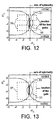
- the reference 56 designates the locations of two gates disposed in an optimum positioning.
- the reference 57 designates the location of a single gate disposed in an optimum position.
- the gates disposed on the locations 56 and 57 enclose the zone where the nanowire has a minimum radius, which affords better control of the current by the gate.
- the parts of the nanowire broadened and close to the contacts are not under the gate, which minimises the access resistances.
- the advantage of having two necks close to each other is to be able to isolate a small quantity of material (the material between the two necks). Manufacturing a single gate covering the two neck zones would make it possible to obtain an effect of the transistor type with one or more electrons (see FIG. 13 ).
- FIGS. 14A and 14B depict attachment zones between nanowires and their corresponding contact according to the known art ( FIG. 14A ) and according to the invention ( FIG. 14B ).
- FIG. 14A shows nanowires 61 attached to their contact 62 at an angle ⁇ forming 90°.
- FIG. 14B shows nanowires 71 attached to their contact 72 at an angle ⁇ forming 45°: the shape of the nanowires is therefore splayed in its connection with their contact. Under these conditions, the rupture time of a nanowire is pushed back by a factor greater than 2 as illustrated in FIG. 15 .
- FIG. 15 is a graph showing the minimum of the radius of the nanowire at the neck, r neck , as a function of the time t, the coefficient B and the initial radius of the nanowire r 0 for the geometries shown in FIGS. 14A and 14B .
- the modification of the geometry close to the contacts thus makes it possible to push back the rupture time and enables the experimenter to choose the time and temperature of the annealing within less constraining ranges for which rupture is not caused by the annealing.
- Another advantage is a gain on the technological variability. For example, for a time 0.5 r 0 4 /B, a geometry at 90° according to FIG. 14A will cause a necking of 0.65 r 0 , whereas at this same time a geometry at 45° according to FIG. 14B will cause a necking of only 0.85 r 0 (see points A and B on the graph in FIG. 15 ).
Landscapes
- Engineering & Computer Science (AREA)
- Chemical & Material Sciences (AREA)
- Nanotechnology (AREA)
- Physics & Mathematics (AREA)
- Mathematical Physics (AREA)
- Theoretical Computer Science (AREA)
- Crystallography & Structural Chemistry (AREA)
- Thin Film Transistor (AREA)
- Battery Electrode And Active Subsutance (AREA)
Abstract
Description
B=D s·ν·γ·Ω2 /k B ·T
where:
l i=√{square root over ((r i+1 −r i)2+(z i+1 −z 1)2)}{square root over ((r i+1 −r i)2+(z i+1 −z 1)2)}
K 1,i=(r i+1 −r i−1)(r i+1 +r i +r i−1)
K 2,i=−2r i(z i+1 −z i−1)+z i(r i+1 −r i−1)−z i+1 r i+1 +z i−1 r i−1
δN i=π[(r i−1 +r i)J i−1−(r i +r i+1)J i ]dt
where (Nr,i, Nz,i) are the coordinates of the vector normal to the iso-volume curve in Mi:
Claims (9)
Applications Claiming Priority (2)
| Application Number | Priority Date | Filing Date | Title |
|---|---|---|---|
| FR0758933A FR2923652B1 (en) | 2007-11-09 | 2007-11-09 | METHOD FOR MANUFACTURING PARALLEL NANOWILS WITH THEIR SUPPORT SUBSTRATE |
| FR0758933 | 2007-11-09 |
Publications (2)
| Publication Number | Publication Date |
|---|---|
| US20090124050A1 US20090124050A1 (en) | 2009-05-14 |
| US8252636B2 true US8252636B2 (en) | 2012-08-28 |
Family
ID=39144329
Family Applications (1)
| Application Number | Title | Priority Date | Filing Date |
|---|---|---|---|
| US12/267,431 Expired - Fee Related US8252636B2 (en) | 2007-11-09 | 2008-11-07 | Method of manufacturing nanowires parallel to the supporting substrate |
Country Status (3)
| Country | Link |
|---|---|
| US (1) | US8252636B2 (en) |
| EP (1) | EP2058847A1 (en) |
| FR (1) | FR2923652B1 (en) |
Families Citing this family (4)
| Publication number | Priority date | Publication date | Assignee | Title |
|---|---|---|---|---|
| FR2910456B1 (en) * | 2006-12-21 | 2018-02-09 | Commissariat A L'energie Atomique | METHOD FOR PRODUCING MICROFILS AND / OR NANOWIAS |
| FR2910455B1 (en) * | 2006-12-21 | 2009-04-03 | Commissariat Energie Atomique | METHOD FOR PRODUCING NON-ALIGNED MICRO-CAVITIES AND DIFFERENT DEPTHS |
| FR2995450A1 (en) * | 2012-09-11 | 2014-03-14 | Centre Nat Rech Scient | Logic gate e.g. NAND-type logic gate, for manufacturing part of locally constricted FET in digital electronic industry, has grid whose portion is positioned relative to zones so as to have field effect when channel is traversed by current |
| US9048301B2 (en) | 2013-10-16 | 2015-06-02 | Taiwan Semiconductor Manufacturing Company Limited | Nanowire MOSFET with support structures for source and drain |
Citations (5)
| Publication number | Priority date | Publication date | Assignee | Title |
|---|---|---|---|---|
| US20040166642A1 (en) * | 2003-02-20 | 2004-08-26 | Hao-Yu Chen | Semiconductor nano-rod devices |
| US20050275010A1 (en) | 2004-06-10 | 2005-12-15 | Hung-Wei Chen | Semiconductor nano-wire devices and methods of fabrication |
| US20060214212A1 (en) * | 2005-03-23 | 2006-09-28 | Renesas Technology Corp. | Semiconductor device and method of manufacturing semiconductor device |
| DE102006012416A1 (en) | 2005-03-24 | 2006-10-05 | Samsung Electronics Co., Ltd., Suwon | Field effect transistor fabrication involves etching and annealing nano-wire channel region extended between source and drain regions |
| US20070222353A1 (en) * | 2004-07-16 | 2007-09-27 | The Trustees Of Boston College | Device and method for achieving enhanced field emission utilizing nanostructures grown on a conductive substrate |
-
2007
- 2007-11-09 FR FR0758933A patent/FR2923652B1/en not_active Expired - Fee Related
-
2008
- 2008-11-05 EP EP08168359A patent/EP2058847A1/en not_active Withdrawn
- 2008-11-07 US US12/267,431 patent/US8252636B2/en not_active Expired - Fee Related
Patent Citations (5)
| Publication number | Priority date | Publication date | Assignee | Title |
|---|---|---|---|---|
| US20040166642A1 (en) * | 2003-02-20 | 2004-08-26 | Hao-Yu Chen | Semiconductor nano-rod devices |
| US20050275010A1 (en) | 2004-06-10 | 2005-12-15 | Hung-Wei Chen | Semiconductor nano-wire devices and methods of fabrication |
| US20070222353A1 (en) * | 2004-07-16 | 2007-09-27 | The Trustees Of Boston College | Device and method for achieving enhanced field emission utilizing nanostructures grown on a conductive substrate |
| US20060214212A1 (en) * | 2005-03-23 | 2006-09-28 | Renesas Technology Corp. | Semiconductor device and method of manufacturing semiconductor device |
| DE102006012416A1 (en) | 2005-03-24 | 2006-10-05 | Samsung Electronics Co., Ltd., Suwon | Field effect transistor fabrication involves etching and annealing nano-wire channel region extended between source and drain regions |
Non-Patent Citations (4)
| Title |
|---|
| Pennelli et al., "Silicon Single-electron Transistor Fabricated by Anisotropic Etch and Oxidation," Microelectronic Engineering 83:1710-13 (2006). |
| Preliminary Search Report for International Patent Application No. FR 0758933 (Mar. 10, 2008). |
| Takashi et al., "Multigate Single-electron Transistors and Their Application to an Exclusive-OR Gate," Applied Physics Letters 76(5):637-9 (2000). |
| Zhuang et al., "Silicon Single-electron Quantum-dot Transistor Switch Operating at Room Temperature," Applied Physics Letters 72(10):1205-7 (1998). |
Also Published As
| Publication number | Publication date |
|---|---|
| US20090124050A1 (en) | 2009-05-14 |
| FR2923652B1 (en) | 2010-06-11 |
| FR2923652A1 (en) | 2009-05-15 |
| EP2058847A1 (en) | 2009-05-13 |
Similar Documents
| Publication | Publication Date | Title |
|---|---|---|
| US7685543B2 (en) | Simulation apparatus and simulation method used to design characteristics and circuits of semiconductor device, and semiconductor device fabrication method | |
| DE112013000360B4 (en) | Method for producing a semiconductor unit with a low-k spacer | |
| US6441392B1 (en) | Device based on quantic islands and method for making same | |
| US8252636B2 (en) | Method of manufacturing nanowires parallel to the supporting substrate | |
| Molas et al. | Single electron effects and structural effects in ultrascaled silicon nanocrystal floating-gate memories | |
| Huckemann et al. | Industrially fabricated single-electron quantum dots in si/si–ge heterostructures | |
| Cordan et al. | Electron transport in metallic dot arrays: Effect of a broad dispersion in the tunnel junction dimensions | |
| Morgan et al. | Evidence for activated conduction in a single electron transistor | |
| Carrillo-Nunez et al. | Impact of randomly distributed dopants on $\Omega $-gate junctionless silicon nanowire transistors | |
| Asenov et al. | Effect of oxide interface roughness on the threshold voltage fluctuations in decanano MOSFETs with ultrathin gate oxides | |
| JP4253114B2 (en) | Manufacturing method of SET element | |
| Wang et al. | Single-electron and quantum confinement limits in length-scaled silicon nanowires | |
| Suñé et al. | Temperature dependence of Fowler-Nordheim injection from accumulated n-type silicon into silicon dioxide | |
| US7217946B2 (en) | Method for making a wire nanostructure in a semiconductor film | |
| US6285970B1 (en) | Computer simulation method of silicon oxidation | |
| Pourghaderi et al. | Universal swing factor approach for performance analysis of logic nodes | |
| Leroy et al. | Variance analysis of the Coulomb blockade parameters in nanometer-size disordered arrays | |
| Thorbeck et al. | Simulating capacitances to silicon quantum dots: Breakdown of the parallel plate capacitor model | |
| Garcıa-Garcıa et al. | Simulation of multilayered resonant tunneling diodes using coupled Wigner and Boltzmann distribution function approaches | |
| Abualnaja | Room Temperature Quantum Dot Transistors in Silicon | |
| Knobloch | Characterization and physical modeling of degradation in MoS2 transistors | |
| Hashemi | Gate-all-around silicon nanowire MOSFETs: top-down fabrication and transport enhancement techniques | |
| Bugliarelli | Vertical Junctionless Nano Transistor TCAD modeling and performance evaluation | |
| Oh et al. | Dielectric Confinement Impact on Electrical Performance of Highly Scaled Saddle-Fin Cell Transistor for High Density DRAM | |
| Grillone | Process Simulation and Compact Modelling for a Vertical Junctionless Nanowire Transistor |
Legal Events
| Date | Code | Title | Description |
|---|---|---|---|
| AS | Assignment |
Owner name: COMMISSARIAT A L'ENERGIE ATOMIQUE, FRANCE Free format text: ASSIGNMENT OF ASSIGNORS INTEREST;ASSIGNORS:DORNEL, ERWAN;BARBE, JEAN-CHARLES;ERNST, THOMAS HAMEAU CHECHAMAIN;REEL/FRAME:022157/0217 Effective date: 20081103 |
|
| ZAAA | Notice of allowance and fees due |
Free format text: ORIGINAL CODE: NOA |
|
| ZAAB | Notice of allowance mailed |
Free format text: ORIGINAL CODE: MN/=. |
|
| STCF | Information on status: patent grant |
Free format text: PATENTED CASE |
|
| FPAY | Fee payment |
Year of fee payment: 4 |
|
| MAFP | Maintenance fee payment |
Free format text: PAYMENT OF MAINTENANCE FEE, 8TH YEAR, LARGE ENTITY (ORIGINAL EVENT CODE: M1552); ENTITY STATUS OF PATENT OWNER: LARGE ENTITY Year of fee payment: 8 |
|
| FEPP | Fee payment procedure |
Free format text: MAINTENANCE FEE REMINDER MAILED (ORIGINAL EVENT CODE: REM.); ENTITY STATUS OF PATENT OWNER: LARGE ENTITY |
|
| LAPS | Lapse for failure to pay maintenance fees |
Free format text: PATENT EXPIRED FOR FAILURE TO PAY MAINTENANCE FEES (ORIGINAL EVENT CODE: EXP.); ENTITY STATUS OF PATENT OWNER: LARGE ENTITY |
|
| STCH | Information on status: patent discontinuation |
Free format text: PATENT EXPIRED DUE TO NONPAYMENT OF MAINTENANCE FEES UNDER 37 CFR 1.362 |
|
| FP | Lapsed due to failure to pay maintenance fee |
Effective date: 20240828 |