US8213722B2 - Method for inspecting critical dimension uniformity at high speed measurement - Google Patents
Method for inspecting critical dimension uniformity at high speed measurement Download PDFInfo
- Publication number
- US8213722B2 US8213722B2 US12/607,238 US60723809A US8213722B2 US 8213722 B2 US8213722 B2 US 8213722B2 US 60723809 A US60723809 A US 60723809A US 8213722 B2 US8213722 B2 US 8213722B2
- Authority
- US
- United States
- Prior art keywords
- photo mask
- pattern
- measurement image
- measurement
- area
- Prior art date
- Legal status (The legal status is an assumption and is not a legal conclusion. Google has not performed a legal analysis and makes no representation as to the accuracy of the status listed.)
- Active, expires
Links
- 238000005259 measurement Methods 0.000 title claims abstract description 83
- 238000000034 method Methods 0.000 title claims abstract description 32
- 230000002093 peripheral effect Effects 0.000 claims description 13
- 238000013461 design Methods 0.000 claims description 6
- 230000003287 optical effect Effects 0.000 abstract description 23
- 238000004519 manufacturing process Methods 0.000 abstract description 6
- 101100269850 Caenorhabditis elegans mask-1 gene Proteins 0.000 description 33
- 238000010894 electron beam technology Methods 0.000 description 3
- 238000002513 implantation Methods 0.000 description 3
- 230000003247 decreasing effect Effects 0.000 description 2
- 239000006185 dispersion Substances 0.000 description 2
- 238000007689 inspection Methods 0.000 description 2
- 238000012986 modification Methods 0.000 description 2
- 230000004048 modification Effects 0.000 description 2
- 238000000206 photolithography Methods 0.000 description 2
- 239000004065 semiconductor Substances 0.000 description 2
- 230000007547 defect Effects 0.000 description 1
- 239000007943 implant Substances 0.000 description 1
- 238000011835 investigation Methods 0.000 description 1
- 239000000463 material Substances 0.000 description 1
- 238000000691 measurement method Methods 0.000 description 1
- 239000000203 mixture Substances 0.000 description 1
- 230000007261 regionalization Effects 0.000 description 1
Images


Classifications
-
- G—PHYSICS
- G03—PHOTOGRAPHY; CINEMATOGRAPHY; ANALOGOUS TECHNIQUES USING WAVES OTHER THAN OPTICAL WAVES; ELECTROGRAPHY; HOLOGRAPHY
- G03F—PHOTOMECHANICAL PRODUCTION OF TEXTURED OR PATTERNED SURFACES, e.g. FOR PRINTING, FOR PROCESSING OF SEMICONDUCTOR DEVICES; MATERIALS THEREFOR; ORIGINALS THEREFOR; APPARATUS SPECIALLY ADAPTED THEREFOR
- G03F1/00—Originals for photomechanical production of textured or patterned surfaces, e.g., masks, photo-masks, reticles; Mask blanks or pellicles therefor; Containers specially adapted therefor; Preparation thereof
- G03F1/68—Preparation processes not covered by groups G03F1/20 - G03F1/50
- G03F1/82—Auxiliary processes, e.g. cleaning or inspecting
- G03F1/84—Inspecting
- G03F1/86—Inspecting by charged particle beam [CPB]
-
- G—PHYSICS
- G06—COMPUTING; CALCULATING OR COUNTING
- G06T—IMAGE DATA PROCESSING OR GENERATION, IN GENERAL
- G06T7/00—Image analysis
- G06T7/0002—Inspection of images, e.g. flaw detection
- G06T7/0004—Industrial image inspection
- G06T7/0006—Industrial image inspection using a design-rule based approach
-
- G—PHYSICS
- G03—PHOTOGRAPHY; CINEMATOGRAPHY; ANALOGOUS TECHNIQUES USING WAVES OTHER THAN OPTICAL WAVES; ELECTROGRAPHY; HOLOGRAPHY
- G03F—PHOTOMECHANICAL PRODUCTION OF TEXTURED OR PATTERNED SURFACES, e.g. FOR PRINTING, FOR PROCESSING OF SEMICONDUCTOR DEVICES; MATERIALS THEREFOR; ORIGINALS THEREFOR; APPARATUS SPECIALLY ADAPTED THEREFOR
- G03F7/00—Photomechanical, e.g. photolithographic, production of textured or patterned surfaces, e.g. printing surfaces; Materials therefor, e.g. comprising photoresists; Apparatus specially adapted therefor
- G03F7/70—Microphotolithographic exposure; Apparatus therefor
- G03F7/70483—Information management; Active and passive control; Testing; Wafer monitoring, e.g. pattern monitoring
- G03F7/70605—Workpiece metrology
- G03F7/70616—Monitoring the printed patterns
- G03F7/70625—Dimensions, e.g. line width, critical dimension [CD], profile, sidewall angle or edge roughness
-
- G—PHYSICS
- G03—PHOTOGRAPHY; CINEMATOGRAPHY; ANALOGOUS TECHNIQUES USING WAVES OTHER THAN OPTICAL WAVES; ELECTROGRAPHY; HOLOGRAPHY
- G03F—PHOTOMECHANICAL PRODUCTION OF TEXTURED OR PATTERNED SURFACES, e.g. FOR PRINTING, FOR PROCESSING OF SEMICONDUCTOR DEVICES; MATERIALS THEREFOR; ORIGINALS THEREFOR; APPARATUS SPECIALLY ADAPTED THEREFOR
- G03F7/00—Photomechanical, e.g. photolithographic, production of textured or patterned surfaces, e.g. printing surfaces; Materials therefor, e.g. comprising photoresists; Apparatus specially adapted therefor
- G03F7/70—Microphotolithographic exposure; Apparatus therefor
- G03F7/70483—Information management; Active and passive control; Testing; Wafer monitoring, e.g. pattern monitoring
- G03F7/70605—Workpiece metrology
- G03F7/70653—Metrology techniques
- G03F7/70666—Aerial image, i.e. measuring the image of the patterned exposure light at the image plane of the projection system
-
- G—PHYSICS
- G06—COMPUTING; CALCULATING OR COUNTING
- G06T—IMAGE DATA PROCESSING OR GENERATION, IN GENERAL
- G06T2207/00—Indexing scheme for image analysis or image enhancement
- G06T2207/30—Subject of image; Context of image processing
- G06T2207/30108—Industrial image inspection
- G06T2207/30148—Semiconductor; IC; Wafer
Definitions
- the inventive concept relates to a reliability inspecting method in a high-speed measurement of a fine pattern, and more particularly, a method for inspecting reliability in a high-speed measurement of a fine pattern formed in a photo mask at a high speed.
- a design rule of integrated circuits is being reduced to 0.1 micro or below as semiconductor devices are increasingly becoming highly integrated.
- various processes are required and margins are increasingly becoming reduced. For example, increasing difficulty in a photolithography processes may cause a serious influence on a wafer due to even small change of a photo mask, and thus an overall investigation for various patterns should be executed on an overall photo mask.
- the photo mask undergoes a precise measurement using an electron microscope.
- the photo mask needs to measure by thousands of points or more for the overall photo mask.
- an electron microscope SEM is valid to measure just for sampled-pattern at a level of tens of points owing to a speed question. It is also impossible in principle to measure a step coverage or material difference of a photo mask influencing a wafer pattern, an optical difference through an incline of pattern etc., by using an electron microscope.
- the photo mask is measured at a high speed by using an optical microscope such as an aerial image inspection device.
- a high-speed measurement method using an optical microscope is to detect a uniformity of a critical dimension (hereinafter, referred to as ‘CD’) of a photo mask pattern by deciding a repetition section for a repeated pattern and obtaining the sum of images therefor and then performing their relative comparison.
- CD critical dimension
- some embodiments of the present invention provide a method for inspecting a CD uniformity of photo mask, which is capable of ensuring a high signal in comparison with noise even when an open density of pattern in a repetition section is relatively low, and simply inspecting a CD uniformity of a photo mask pattern, thereby increasing a production yield.
- the productivity can substantially increase by more precisely performing a measurement of high speed for a photo mask.
- a method for inspecting a uniformity of CD of a photo mask pattern comprises obtaining information for a CD of pattern formed in the photo mask by precisely measuring the photo mask; obtaining a plurality of measurement images having the pattern by photographing the photo mask at a high speed; capturing respective pattern areas provided in the plurality of measurement images; calculating a gray level value of the pattern area; confirming an estimated value corresponding to a change of the gray level value based on the CD of the precision measurement; and confirming the uniformity of the CD at a measurement of high speed by checking a range the gray level value is deviated from the estimated value.
- the method may further comprise deciding whether an open density of the measurement image is relatively low, and calculating the estimated value corresponding to the change of the gray level value got being based on the CD of the precision measurement.
- the estimated value may be represented as a linear equation, and the uniformity of the CD may be represented as a correlation coefficient.
- a pattern area is captured in an image measured at a high speed through an optical microscope and thus a high signal in comparison with noise can be ensured, and a uniformity of CD of photo mask can be simply inspected, thereby substantially increasing a production yield.
- Productivity can substantially increase by calculating a CD uniformity of a photo mask and more precisely performing a high-speed measurement of a photo mask.
- FIGS. 1A and 1B schematically illustrate an electron microscope and an optical microscope
- FIG. 2 is a flowchart providing a CD uniformity inspecting method of the photo mask according to an embodiment of the present invention
- FIG. 3 is a plan view illustrating a photo mask having a relatively high open density
- FIG. 4 is a graph providing an open density of FIG. 3 as a gray level value
- FIG. 5 is an enlarged plan view of photo mask with a relatively low open density:
- FIG. 6 is a graph of providing, as a gray level value, an open density referred to in FIG. 5 :
- FIGS. 7A and 7B are plan views illustrating a capturing of pattern area in measurement image:
- FIG. 8 is a graph got through a comparison of uniformity for a CD containing a noise signal with uniformity for a CD with a removal of noise signal.
- first, second, third etc. may be used herein to describe various elements, components, regions, layers and/or sections, these elements, components, regions, layers and/or sections should not be limited by these terms. These terms are only used to distinguish one element, component, region, layer or section from another region, layer or section. Thus, a first element, component, region, layer or section discussed below could be termed a second element, component, region, layer or section without departing from the teachings of the present invention.
- spatially relative terms such as “beneath,” “below,” “lower,” “above,” “upper” and the like, may be used herein for ease of description to describe one element or feature's relationship to another element(s) or feature(s) as illustrated in the figures. It will be understood that the spatially relative terms are intended to encompass different orientations of the device in use or operation in addition to the orientation depicted in the figures. For example, if the device in the figures is turned over, elements described as “below” or “beneath” other elements or features would then be oriented “above” the other elements or features. Thus, the exemplary term “below” can encompass both an orientation of above and below.
- the structure and/or the device may be otherwise oriented (rotated 90 degrees or at other orientations) and the spatially relative descriptors used herein interpreted accordingly.
- Example embodiments of the present invention are described herein with reference to cross-section illustrations that are schematic illustrations of idealized embodiments (and intermediate structures) of the present invention. As such, variations from the shapes of the illustrations as a result, for example, of manufacturing techniques and/or tolerances, are to be expected. Thus, example embodiments of the present invention should not be construed as limited to the particular shapes of regions illustrated herein but are to include deviations in shapes that result, for example, from manufacturing. For example, an implanted region illustrated as a rectangle will, typically, have rounded or curved features and/or a gradient of implant concentration at its edges rather than a binary change from implanted to non-implanted region.
- a buried region formed by implantation may result in some implantation in the region between the buried region and the surface through which the implantation takes place.
- the regions illustrated in the figures are schematic in nature and their shapes are not intended to illustrate the actual shape of a region of a device and are not intended to limit the scope of the present invention.
- FIGS. 1 to 8 Function and method in embodiments are described in detail referring to FIGS. 1 to 8 .
- FIGS. 1A and 1B schematically illustrate an electron microscope and optical microscope used in embodiments of the present invention.
- a photo mask 1 is measured precisely by using an electron microscope 10 to obtain a CD of a pattern of the photo mask 1 , and the photo mask 1 is measured at a high speed through an optical microscope 20 to confirm or inspect a uniformity of the pattern CD.
- the electron microscope 10 may precisely measure the CD of a pattern formed in the photo mask 1 as an electron beam 13 discharged from an electron source 12 is scattered on the photo mask 1 and then detected by an electron beam detector 14 , thereby precisely measuring the CD of the pattern formed in the photo mask 1 .
- the electron microscope 10 may precisely measure the CD of a pattern by scanning an electron beam 13 having a radius of approximately 2 ⁇ 3 nm on the photo mask 1 .
- the optical microscope 20 can obtain a measurement image by photographing the photo mask 1 by using a sensor 28 , i.e., charge coupled device (CCD), using light 21 passing through the photo mask 1 from a light source 22 .
- a sensor 28 i.e., charge coupled device (CCD)
- CCD charge coupled device
- intensity for a portion of the light is checked through an intensity detector 24 by using a half mirror 23 , and the rest light is mostly exposed to the photo mask 1 .
- the intensity of the light 21 detected by the intensity detector 24 may be used as data in an open density calculation of measurement image.
- the light 21 passing through the photo mask 1 passes through an optical system 26 formed of at least one lens, enlarges and projects the photo mask 1 , and is obtained as a measurement image through a sensor 28 .
- the optical microscope 20 exposes the photo mask 1 to laser light 21 having a diameter of approximately 10 1 ⁇ 10 2 ⁇ m at a time from several positions, thereby acquiring a large quantity of measurement images sequentially, fast.
- the optical microscope 20 can measure various parts of the photo mask 1 at a high speed as compared with the electron microscope 10 .
- a uniformity of CD provided in a measurement image acquired by the optical microscope 20 is inspected by using the CD of the photo mask 1 detected through the electron microscope 10 as reference data.
- FIG. 2 is a flow chart providing a uniformity inspecting method of CD of the photo mask according to an embodiment of the present invention.
- the photo mask 1 is precisely measured in a step S 10 , by using electron microscope 10 .
- Various sizes of patterns are formed in the photo mask 1 , and the electron microscope 10 can measure the size of pattern.
- the electron microscope 10 sequentially measures the patterns formed in the photo mask 1 according to the size, thereby subsequently using the CD as reference data of a measurement image to be measured through the optical microscope 20 .
- the photo mask 1 is photographed at a high speed by using the optical microscope 20 , thus obtaining a measurement image in a step S 20 .
- the optical microscope 20 does not individually measure patterns formed in the photo mask 1 , but obtains the measurement image by photographing at a time a given number of patterns provided in a corresponding unit area.
- the optical microscope 20 can obtain the measurement image by photographing a screen of approximately 10 3 ⁇ 10 5 ⁇ m 2 in the size in a stepper type.
- the measurement image comprises a plurality of patterns based on a single size within a square shape and is provided as black-and-white.
- a measurement image is obtained by using the optical microscope 20 , and a uniformity based on the size of a plurality of patterns represented in the measurement image is confirmed, in place of individually confirming the size of patterns represented in the measurement image.
- an open density of measurement image obtained from the optical microscope 20 is relatively low.
- the open density may be decided as a low or high level from the standard of approximately 0.5.
- a pattern of measurement image is relatively large or the number of patterns is relatively many, the open density is high, and when the size of pattern or the number of patterns is relatively small, the open density is low. That is, when the open density is high, a uniformity of the CD using the measurement image can be simply confirmed.
- a gray level value is immediately calculated in a step S 40 .
- the gray level value is a regular value obtained by dividing a light-and-darkness of the measurement image into approximately 256 grades of 0 to 255. This level may be subdivided more in detail depending on the kind of sensors or CCD.
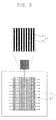
- FIG. 3 is an enlarged plan view illustrating a photo mask 1 having a relatively high open density.
- a central area 2 having a relatively high open density is formed in an outer area 3 .
- the central area 2 is formed of a stripe pattern, and a measurement image indicating the central area 2 is provided with an open density of approximately 0.5.
- the central area 2 comprises a pattern area 4 having a pattern formation, and a peripheral area 5 formed surrounding the pattern area 4 .
- An arrow shown in the drawing indicates a direction of acquiring a measurement image of the central area 2 while the optical microscope 20 moves.
- FIG. 4 is a graph providing an open density of FIG. 3 through a gray level value.
- the measurement image having a high open density is provided proportionately by an incline having a relatively high gray level value as the CD becomes increased.
- a transverse axis denotes a CD and a longitudinal axis indicates a gray level value corresponding to an average intensity of an open area.
- the correlation coefficient R 2 is represented relatively very highly as 0.9872, that is, this denotes that the gray level value in the measurement image is well traced to the estimated value.
- a uniformity of CD in pattern area 4 is confirmed by capturing the pattern area 4 having at least one pattern within the central area 2 of the measurement image.
- FIG. 5 is an enlarged plan view of photo mask 1 with a relatively low open density.
- pattern area 4 is excessively small as compared with peripheral area 5 .
- a peak signal of a light-and-darkness is provided in the pattern area 4
- a noise signal is provided in the peripheral area 5 .
- the measurement image is formed mostly of peripheral area 5 of a black in which the light 21 is cut off, and is formed of a pattern area 4 as the rest through which the light 21 passes.
- FIG. 6 is a graph providing, as a gray level value, an open density referred to in FIG. 5 .
- a gray level value is not almost changed or is provided in proportionate to a relatively low incline even when the CD increases. That is, a peak signal of a light-and-darkness corresponding to the pattern area 4 is not distinguished, but is mixed by the noise signal.
- the correlation coefficient R 2 is represented relatively very lowly as 0.4809, that is, this denotes that the gray level value in the measurement image is not well traced to the estimated value. As a result, the measurement image having a low open density may cause a measurement error.
- the pattern area 4 is captured in the central area 2 of the measurement image with a low open density in a step S 50 .
- the capturing of the pattern area 4 may be obtained by removing peripheral area 5 having a noise signal or by selecting pattern area 4 based on a design standard.
- just pattern area 4 is captured by selecting a peak signal having a level higher than noise signal in the measurement image.
- the pattern area 4 comprises almost an open area and an adjacent area of the open area.
- the adjacent area partially contains a noise signal, but may have partially a signal of high level with an influence from a peak signal provided in the open area.
- the adjacent area contains a portion in which a peak signal having a level higher by approximately 10% ⁇ 20% than a noise signal is represented. Accordingly, in the embodiment, even when the open density of pattern is relatively low within the repetition section, a peak signal of high level as compared with a noise signal is ensured, and thus a uniformity of CD of the photo mask 1 can be simply inspected.
- FIGS. 7A and 7B are plan views illustrating a capturing of pattern area 4 in a measurement image.
- central area 2 of measurement image is formed of pattern area 4 and peripheral area 5 .
- the pattern area 4 may be captured except the peripheral area 5 having a noise signal within the measurement image.
- the pattern area 4 is an area where a peak signal and a noise signal exist together in the measurement image, and is provided with almost peak signals.
- the pattern area 4 is captured in a rectangle type in the measurement image.
- the pattern area 4 may be captured as several shapes since the pattern areas 4 provided in the measurement image may become different from one another.
- a noise signal appearing in the peripheral area 5 is removed by capturing the pattern area 4 having just a peak signal in the measurement image, and thus a gray level value is calculated.
- the uniformity of CD for the open area formed of just the pattern area 4 having just a peak signal can be detected, thereby increasing a precision of the inspection.
- pattern area 4 provided in an initial design of photo mask 1 may be captured in measurement image.
- the pattern area 4 requires information for an area predetermined in the design of the photo mask 1 . That is, when a measurement image and a design image of the photo mask 1 accord with each other, the pattern area 4 can be captured in the measurement image according to a predetermined standard.
- a gray level value of the captured pattern area 4 is calculated in a step S 60 .
- the pattern area 4 has just a peak signal, thus the gray level value is relatively high therein. This is why the gray level value is calculated by using just a peak signal except the peripheral area 5 having a noise signal as described above.
- the gray level value for the overall measurement image may be obtained by dividing a value obtained by adding up the noise signal and the peak signal of the peripheral area 5 and the pattern area 4 , by an area.
- the gray level value of the overall measurement image having the noise signal and the peak signal is obtained as a low level since a loss is generated in the value divided by the area of the measurement image.
- the gray level value in the pattern area 4 is provided being regarded with just the pattern area 4 , regardless of the peripheral area 5 having a noise signal, and thus can have a relatively high value.
- An estimated value corresponding to a change of gray level value based on the pattern size obtained in the precision measurement is calculated in a step S 70 .
- the pattern may be decided being classified as a relatively smaller size of pattern and a relatively larger size of pattern from the standard of a specific sized. As the size of pattern increases, the open area becomes large, thus the gray level value increases.
- the estimated value is represented in a linear equation defined as a proportional-relational expression thereof. That is, an estimated value of linear equation is obtained through a proportion of the gray level value based on the CD.
- the correlation coefficient R 2 may be represented as the following numerical expression 1.
- R 2 1 ⁇ SS err /SS tot (Numerical Expression 1)
- SS tot is represented as ⁇ (y i ⁇ y) 2 , and indicates the total dispersion value, and is represented as the sum of SS reg and SS err as the total sum of squares.
- SS reg is represented as ⁇ (f i ⁇ f) 2 as a regression sum of squares.
- SS err is represented as ⁇ (y i ⁇ f) 2 as a sum of squared errors or a residual sum of squares.
- a correlation coefficient R 2 becomes increased when the sum of squared errors becomes decreased, and furthermore, becomes increased when the total dispersion value becomes increased. Therefore, when an extent that the gray level value based on the CD is deviated from an estimated value becomes increased, the correlation coefficient R 2 becomes decreased, and when coinciding with the estimated value, the correlation coefficient R 2 becomes increased.
- a measurement state of the photo mask 1 using the optical microscope 20 is decided according to a value of correlation coefficient in a step S 90 .
- the correlation coefficient R 2 has a given level or more, it is decided that a measurement process of the photo mask 1 is dominant, such that a user recognizes a normal manufacture of the photo mask 1 by representing an estimated value and the correlation coefficient R 2 in a graph, and thus a photolithography process using the photo mask 1 is performed in a step S 100 .
- the correlation coefficient R 2 is less than a predetermined value, the pattern area 4 captured in the measurement image measured at a high speed through the optical microscope 20 is relatively small.
- FIG. 8 is a graph obtained through a comparison of uniformity for a CD having a noise signal with uniformity for a CD from which a noise signal has been removed.
- an X-axis indicates the size of pattern with a small size or large size from the standard pattern of approximately 150 nm.
- a pattern of 140 nm is provided as ⁇ 10 nm
- a pattern of 160 nm is provided as +10 nm.
- a gray level value provided on a y-axis is divided into grades of 0 to 255.
- a more prominent uniformity in a CD of photo mask 1 can be acquired, by capturing pattern area 4 with a removal of noise signal in the measurement image and then calculating a gray level value based on a CD, rather than investigating a gray level value based on a CD through use of measurement image intact with a low open density.
- a gray level value is obtained by capturing just the pattern area 4 from the measurement image and thus an estimated value and a correlation coefficient R 2 are calculated, thereby attaining a more precise measurement process as compared with obtaining a gray level value using just a measurement image and increasing reliability in the measurement process.
Landscapes
- Physics & Mathematics (AREA)
- General Physics & Mathematics (AREA)
- Engineering & Computer Science (AREA)
- Quality & Reliability (AREA)
- Computer Vision & Pattern Recognition (AREA)
- Theoretical Computer Science (AREA)
- Testing Or Measuring Of Semiconductors Or The Like (AREA)
- Preparing Plates And Mask In Photomechanical Process (AREA)
- Investigating Materials By The Use Of Optical Means Adapted For Particular Applications (AREA)
Abstract
Description
R 2=1−SS err /SS tot (Numerical Expression 1)
Claims (10)
Applications Claiming Priority (2)
| Application Number | Priority Date | Filing Date | Title |
|---|---|---|---|
| KR10-2008-0108789 | 2008-11-04 | ||
| KR1020080108789A KR101385753B1 (en) | 2008-11-04 | 2008-11-04 | Method for inspecting critical dimension uniformity at the high speed measurement |
Publications (2)
| Publication Number | Publication Date |
|---|---|
| US20100111427A1 US20100111427A1 (en) | 2010-05-06 |
| US8213722B2 true US8213722B2 (en) | 2012-07-03 |
Family
ID=42131484
Family Applications (1)
| Application Number | Title | Priority Date | Filing Date |
|---|---|---|---|
| US12/607,238 Active 2031-02-24 US8213722B2 (en) | 2008-11-04 | 2009-10-28 | Method for inspecting critical dimension uniformity at high speed measurement |
Country Status (2)
| Country | Link |
|---|---|
| US (1) | US8213722B2 (en) |
| KR (1) | KR101385753B1 (en) |
Cited By (2)
| Publication number | Priority date | Publication date | Assignee | Title |
|---|---|---|---|---|
| US9897554B2 (en) | 2015-06-03 | 2018-02-20 | Samsung Electronics Co., Ltd. | Method of inspecting surface and method of inspecting photomask using the same |
| US11023770B2 (en) * | 2019-09-23 | 2021-06-01 | Hong Kong Applied Science And Technology Research Institute Co., Ltd. | Systems and methods for obtaining templates for tessellated images |
Families Citing this family (3)
| Publication number | Priority date | Publication date | Assignee | Title |
|---|---|---|---|---|
| CN103713471B (en) * | 2012-10-08 | 2016-03-09 | 合肥京东方光电科技有限公司 | A kind of means for correcting of key size measuring and method |
| CN103852976B (en) * | 2014-04-01 | 2016-01-20 | 海迪科(苏州)光电科技有限公司 | For the method for periodicity litho pattern size monitoring |
| KR102674578B1 (en) | 2019-08-06 | 2024-06-12 | 삼성디스플레이 주식회사 | Method for measuring critical dimension of photo resist pattern |
Citations (6)
| Publication number | Priority date | Publication date | Assignee | Title |
|---|---|---|---|---|
| KR20050063325A (en) | 2003-12-22 | 2005-06-28 | 주식회사 하이닉스반도체 | Critical dimension measurement method for mask using scanning electron microscope |
| JP2005285898A (en) | 2004-03-29 | 2005-10-13 | Toppan Printing Co Ltd | Pattern image determination method and pattern image determination apparatus using the same |
| US20060147818A1 (en) * | 2005-01-04 | 2006-07-06 | Myoung-Soo Lee | Method of correcting deviations of critical dimensions of patterns formed on a wafer in a EUVL process |
| KR100721729B1 (en) | 2006-06-15 | 2007-05-25 | 삼성전자주식회사 | Method and apparatus for measuring a critical dimension of a pattern |
| US20080260234A1 (en) * | 2007-03-19 | 2008-10-23 | Advanced Mask Inspection Technology | Pattern inspection apparatus, corrected image generation method, and computer-readable recording medium storing program |
| US7865866B2 (en) * | 2007-05-16 | 2011-01-04 | Samsung Electronics Co., Ltd. | Method of inspecting mask using aerial image inspection apparatus |
Family Cites Families (1)
| Publication number | Priority date | Publication date | Assignee | Title |
|---|---|---|---|---|
| JPH10177589A (en) * | 1996-12-18 | 1998-06-30 | Mitsubishi Electric Corp | Pattern comparison inspection device, its method, and medium recording pattern comparing and verifying program |
-
2008
- 2008-11-04 KR KR1020080108789A patent/KR101385753B1/en active IP Right Grant
-
2009
- 2009-10-28 US US12/607,238 patent/US8213722B2/en active Active
Patent Citations (6)
| Publication number | Priority date | Publication date | Assignee | Title |
|---|---|---|---|---|
| KR20050063325A (en) | 2003-12-22 | 2005-06-28 | 주식회사 하이닉스반도체 | Critical dimension measurement method for mask using scanning electron microscope |
| JP2005285898A (en) | 2004-03-29 | 2005-10-13 | Toppan Printing Co Ltd | Pattern image determination method and pattern image determination apparatus using the same |
| US20060147818A1 (en) * | 2005-01-04 | 2006-07-06 | Myoung-Soo Lee | Method of correcting deviations of critical dimensions of patterns formed on a wafer in a EUVL process |
| KR100721729B1 (en) | 2006-06-15 | 2007-05-25 | 삼성전자주식회사 | Method and apparatus for measuring a critical dimension of a pattern |
| US20080260234A1 (en) * | 2007-03-19 | 2008-10-23 | Advanced Mask Inspection Technology | Pattern inspection apparatus, corrected image generation method, and computer-readable recording medium storing program |
| US7865866B2 (en) * | 2007-05-16 | 2011-01-04 | Samsung Electronics Co., Ltd. | Method of inspecting mask using aerial image inspection apparatus |
Cited By (2)
| Publication number | Priority date | Publication date | Assignee | Title |
|---|---|---|---|---|
| US9897554B2 (en) | 2015-06-03 | 2018-02-20 | Samsung Electronics Co., Ltd. | Method of inspecting surface and method of inspecting photomask using the same |
| US11023770B2 (en) * | 2019-09-23 | 2021-06-01 | Hong Kong Applied Science And Technology Research Institute Co., Ltd. | Systems and methods for obtaining templates for tessellated images |
Also Published As
| Publication number | Publication date |
|---|---|
| KR20100049799A (en) | 2010-05-13 |
| US20100111427A1 (en) | 2010-05-06 |
| KR101385753B1 (en) | 2014-04-17 |
Similar Documents
| Publication | Publication Date | Title |
|---|---|---|
| JP5254270B2 (en) | Inspection method and inspection apparatus | |
| JP6043662B2 (en) | Inspection method and inspection apparatus | |
| KR101768493B1 (en) | Mask inspection aaparatus, mask evaluation method and mask evaluation system | |
| TWI517210B (en) | Pattern evaluation method and pattern evaluation device | |
| JP4802481B2 (en) | Surface inspection apparatus, surface inspection method, and exposure system | |
| JP4933601B2 (en) | Inspection apparatus and inspection method | |
| US20060233434A1 (en) | Method and apparatus for inspection | |
| US8213722B2 (en) | Method for inspecting critical dimension uniformity at high speed measurement | |
| JP5514754B2 (en) | Inspection apparatus and inspection method | |
| US20030174876A1 (en) | Local bias map using line width measurements | |
| US9626755B2 (en) | Mask inspection apparatus and mask inspection method | |
| JP6263358B2 (en) | Inspection method and inspection apparatus | |
| JP2013120101A (en) | Inspection device | |
| KR101104665B1 (en) | Substrate inspection system, substrate inspection method and substrate inspection apparatus | |
| JP5010701B2 (en) | Inspection apparatus and inspection method | |
| TWI814165B (en) | Defect Inspection Method | |
| JP2007298501A (en) | Method for adjusting focus, apparatus using the same method, and wafer for use in the same method | |
| JP2011129624A (en) | Method of diagnosing fault of charged particle beam lithography system | |
| TWI686673B (en) | Inspection Method | |
| JP2004151622A (en) | Inspecting apparatus of mask defect and method for inspecting mask defect | |
| JP4131728B2 (en) | Image creation method, image creation apparatus, and pattern inspection apparatus | |
| JP6851178B2 (en) | Pattern inspection method and pattern inspection equipment |
Legal Events
| Date | Code | Title | Description |
|---|---|---|---|
| AS | Assignment |
Owner name: SAMSUNG ELECTRONICS CO., LTD.,KOREA, REPUBLIC OF Free format text: ASSIGNMENT OF ASSIGNORS INTEREST;ASSIGNORS:KIM, HEE-BOM;LEE, MYOUNG-SOO;SUNG, YOUNG-SU;REEL/FRAME:023434/0504 Effective date: 20091016 Owner name: SAMSUNG ELECTRONICS CO., LTD., KOREA, REPUBLIC OF Free format text: ASSIGNMENT OF ASSIGNORS INTEREST;ASSIGNORS:KIM, HEE-BOM;LEE, MYOUNG-SOO;SUNG, YOUNG-SU;REEL/FRAME:023434/0504 Effective date: 20091016 |
|
| STCF | Information on status: patent grant |
Free format text: PATENTED CASE |
|
| FPAY | Fee payment |
Year of fee payment: 4 |
|
| MAFP | Maintenance fee payment |
Free format text: PAYMENT OF MAINTENANCE FEE, 8TH YEAR, LARGE ENTITY (ORIGINAL EVENT CODE: M1552); ENTITY STATUS OF PATENT OWNER: LARGE ENTITY Year of fee payment: 8 |
|
| MAFP | Maintenance fee payment |
Free format text: PAYMENT OF MAINTENANCE FEE, 12TH YEAR, LARGE ENTITY (ORIGINAL EVENT CODE: M1553); ENTITY STATUS OF PATENT OWNER: LARGE ENTITY Year of fee payment: 12 |