US8203815B2 - System and method to provide transient overvoltage suppression - Google Patents
System and method to provide transient overvoltage suppression Download PDFInfo
- Publication number
- US8203815B2 US8203815B2 US12/387,917 US38791709A US8203815B2 US 8203815 B2 US8203815 B2 US 8203815B2 US 38791709 A US38791709 A US 38791709A US 8203815 B2 US8203815 B2 US 8203815B2
- Authority
- US
- United States
- Prior art keywords
- voltage
- transient
- transistor
- power supply
- internal power
- Prior art date
- Legal status (The legal status is an assumption and is not a legal conclusion. Google has not performed a legal analysis and makes no representation as to the accuracy of the status listed.)
- Active, expires
Links
- 230000001052 transient effect Effects 0.000 title claims abstract description 62
- 230000001629 suppression Effects 0.000 title claims abstract description 25
- 239000003990 capacitor Substances 0.000 claims description 18
- 230000005669 field effect Effects 0.000 claims description 6
- 230000001902 propagating effect Effects 0.000 description 5
- 238000010586 diagram Methods 0.000 description 4
- 238000012544 monitoring process Methods 0.000 description 2
- 239000006227 byproduct Substances 0.000 description 1
- 238000006243 chemical reaction Methods 0.000 description 1
- 238000001514 detection method Methods 0.000 description 1
- 239000000463 material Substances 0.000 description 1
- 238000012986 modification Methods 0.000 description 1
- 230000004048 modification Effects 0.000 description 1
- 238000012358 sourcing Methods 0.000 description 1
Images


Classifications
-
- H—ELECTRICITY
- H02—GENERATION; CONVERSION OR DISTRIBUTION OF ELECTRIC POWER
- H02H—EMERGENCY PROTECTIVE CIRCUIT ARRANGEMENTS
- H02H3/00—Emergency protective circuit arrangements for automatic disconnection directly responsive to an undesired change from normal electric working condition with or without subsequent reconnection ; integrated protection
- H02H3/20—Emergency protective circuit arrangements for automatic disconnection directly responsive to an undesired change from normal electric working condition with or without subsequent reconnection ; integrated protection responsive to excess voltage
- H02H3/202—Emergency protective circuit arrangements for automatic disconnection directly responsive to an undesired change from normal electric working condition with or without subsequent reconnection ; integrated protection responsive to excess voltage for dc systems
-
- H—ELECTRICITY
- H02—GENERATION; CONVERSION OR DISTRIBUTION OF ELECTRIC POWER
- H02H—EMERGENCY PROTECTIVE CIRCUIT ARRANGEMENTS
- H02H3/00—Emergency protective circuit arrangements for automatic disconnection directly responsive to an undesired change from normal electric working condition with or without subsequent reconnection ; integrated protection
- H02H3/02—Details
- H02H3/04—Details with warning or supervision in addition to disconnection, e.g. for indicating that protective apparatus has functioned
- H02H3/044—Checking correct functioning of protective arrangements, e.g. by simulating a fault
Definitions
- the present invention is related to transient voltage suppression, and in particular to a circuit topology for providing transient voltage suppression.
- Transient voltage suppression is employed to prevent temporary spikes in voltage from damaging loads, such as power supplies.
- Various circuit topologies have been devised to provide the desired voltage suppression. For instance, in one topology a transient voltage suppression device clamps the input voltage range of the power supply to a level within the rating of the power supply. However, if the voltage suppression device fails to activate, then the load or power supply will be unprotected from transient voltage surges.
- a field effect transistor In another topology, a field effect transistor (FET) is provided in series with the input line providing power to the load (i.e., the high-side of the load, as opposed to the return line or low-side of the load). During a detected transient voltage surge, the FET is turned OFF to cause the transient voltage to be developed across the series FET. Either N-channel or P-channel FETs may be used. The drawback of an N-channel FET is that the gate voltage must be higher than the input line voltage provided at the drain of the FET. As a result, an artificially high gate voltage (i.e., voltage higher than the output voltage being supplied by the power supply) is required to operate the FET in the ON position. Typically, a charge pump and/or transformer is used to generate the gate voltage for the FET, but the conversion to alternating current for transformer operation and/or rapid switching for charge pump operation tends to generate undesirable radio frequency emissions.
- the N-channel FET may be replaced with a P-channel FET.
- the P-channel FET is limited to circuits with relatively small power needs because of the relatively high ON resistance and associated power dissipation generated by the P-channel FET while operating in the normal ON state.
- a transient overvoltage protection circuit prevents transient voltages from propagating to and otherwise damaging a load.
- the protection circuit includes a high-side input for connection to a positive terminal of an external power source, a high-side output for connection to a positive terminal of the load, a low-side input for connection to a negative terminal of the external power source, and a low-side output for connection to a negative terminal of the load.
- a transistor is connected in series between the low-side input and the low-side output.
- a control circuit is connected to monitor the voltage at the high-side input and in response to a detected overvoltage transient turns the transistor OFF.
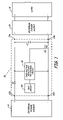
- FIG. 1 is a block diagram of a transient voltage suppression system according to an embodiment of the present invention.
- FIG. 2 is a block/circuit diagram illustrating in more detail a transient voltage suppression system according to an embodiment of the present invention.
- a transient voltage suppression system employs an N-channel field effect transistor (FET) connected in series with the return (i.e., low-side) of a power source.
- FET field effect transistor
- the low-side FET remains ON during normal operation, but in response to a detected high-voltage condition is turned OFF to prevent the transient voltage from propagating to the power supply.
- FIG. 1 is a block diagram of transient voltage suppression circuit 10 according to an embodiment of the present invention connected between external power source 12 and internal power supply 14 , which in turn is connected to provide power to load 16 .
- Suppression circuit 10 includes overvoltage detection logic/FET control logic (hereinafter “control logic”) 18 , test circuit 20 , FET Q 1 , capacitor C 1 and diode D 1 .
- control logic overvoltage detection logic/FET control logic
- Transient voltage suppression circuit 10 includes high-side input terminal 22 a for connection to the positive terminal of external power source 12 and low-side input terminal 22 b for connection to the negative terminal or return of external power source 12 .
- Suppression circuit 10 further includes high-side output terminal 24 a for connection to the positive terminal of internal power supply 14 and low-side output terminal 24 b for connection to the negative terminal of internal power supply 14 .
- transient voltage suppression circuit 10 is employed on-board an aircraft in which external power source 12 provides power derived from an aircraft engine, an auxiliary power unit (APU), and/or a battery supply.
- external power source 12 provides power derived from an aircraft engine, an auxiliary power unit (APU), and/or a battery supply.
- twenty-eight volt direct-current (DC) power is distributed from external power sources (such as external power source 12 ) to one or more loads and/or internal power supplies (such as internal power supply 14 ).
- internal power supplies are employed to convert the power provided by an external power source (e.g., twenty-eight volts) to a voltage appropriate for consumption by a load.
- power from external power source 12 is provided directly to load 16 without being converted by internal power supply 14 .
- Transistor Q 1 is connected in series between low-side input terminal 22 b and low-side output terminal 24 b .
- transistor Q 1 is connected in series between the negative terminal of external power source 12 and the negative terminal of internal power supply 14 (i.e., the return associated with external power source 12 ).
- Control logic circuit 18 is connected to monitor the voltage on high-side input terminal 22 a and selectively controls the state of transistor Q 1 based on the monitored voltage.
- Test circuit 20 is connected to provide input to control logic 18 to ensure that control logic 18 and transistor Q 1 are working properly.
- Capacitor C 1 is connected between high-side output 24 a and low-side output 24 b in parallel with internal power supply 14 .
- a transient voltage condition such as a lightning strike, results in a sudden spike in the high-side voltage monitored by control logic circuit 18 .
- transistor Q 1 is turned OFF to isolate internal power supply 14 from the transient.
- opening transistor Q 1 creates an open-circuit condition that prevents current from propagating from high-side input 22 a to the positive terminal of internal power supply 14 (as well as preventing return current from propagating from low-side input 24 a back to external power source 12 ).
- a transient voltage exists at high-side input 22 a , this transient voltage is not placed across internal power supply 14 .
- the resulting voltage transient is placed across the drain to source of transistor Q 1 , which must be selected to withstand the expected voltage transient magnitude.
- transistor Q 1 which must be selected to withstand the expected voltage transient magnitude.
- FET field effect transistor
- capacitor C 1 is connected in parallel with internal power supply 14 .
- capacitor C 1 is charged by power provided by via high-side input 22 a .
- capacitor C 1 supplies power to internal power supply 14 for the duration of the transient event (typically quite short).
- capacitor C 1 acts to prevent any sudden changes in the voltage seen by internal power supply 14 , thereby protecting internal power supply 14 from the transient voltage while sourcing internal power supply 14 with any current necessary to continue operation until transistor Q 1 is turned ON.
- transistor Q 1 in this embodiment, an N-channel field effect transistor
- transistor Q 1 can be operated without the need for a charge pump or transformer to boost the voltage provided at the gate of transistor Q 1 .
- transistor Q 1 were located on the high-side, turning ON transistor Q 1 would require the voltage provided at the gate of transistor Q 1 to be greater than the voltage provided at high-side input 22 a .
- the voltage provided at high-side input 22 a may be twenty-eight volts or more, which means a charge pump or transformer would be required to boost the twenty-eight volt input to a voltage sufficient to turn ON transistor Q 1 .
- low-side input 22 b is by definition at a lower potential than high-side input 22 a
- the voltage required at the gate of transistor Q 1 to turn the transistor ON may be derived from the input line voltage without need to boost or otherwise increase the voltage level.
- electromagnetic interference which is a by-product of most boosting operations, is reduced.
- transient overvoltage conditions may be symmetrical, meaning that a transient overvoltage condition may result in a large positive voltage at high-side input 22 a or may result in a large negative voltage at high-side input 22 a .
- Control circuit 14 monitors the voltage at high-side input 22 a for positive transients, so a large negative voltage would not be detected.
- diode D 1 effectively blocks current as a result of a large negative voltage at high-side input 22 a and prevents discharge of capacitor C 1 that would result in shutdown of internal power supply 14 .
- transistor Q 1 provides protection for the positive transient and diode D 1 provides protection for the negative transient conditions.
- Internal power supply 14 continues to supply power to the load and is not affected or disturbed during the lightning transients.
- test circuit 20 is connected to provide a test signal to control circuit 18 to ensure that control circuit 18 and transistor Q 1 are working properly. Based on the result of the test, the transient overvoltage protection offered by control circuit 18 and transistor Q 1 can be determined. In one embodiment, the outcome of the test is determined by monitoring the voltage across capacitor C 1 (either manually or with additional hardware connected to monitor the voltage across capacitor C 1 ). If transistor Q 1 is successfully opened (i.e., turned OFF) during the test, then the voltage on capacitor C 1 should decrease as internal power supply 14 draws current from capacitor C 1 .
- FIG. 2 is a circuit diagram illustrating in more detail the logic employed by control circuit 18 and test circuit 20 according to an embodiment of the present invention.
- control circuit 18 includes resistors R 1 , R 2 , R 3 , R 4 , and R 5 , diode D 2 , zener diode VR 1 , and comparator AR 1 .
- Test circuit 20 includes switch U 1 connected between a current limited reference voltage input to comparator AR 1 and low-side return 22 b .
- transient voltage suppression circuit 10 includes high-side input 22 a and high-side output 24 a for connecting the positive terminal of external power source 12 to the positive terminal of internal power supply 14 .
- Suppression circuit 10 further includes low-side input 22 b and low-side output 24 b for connecting the negative terminal of external power source 12 to the negative terminal of internal power supply 14 .
- Resistors R 1 and R 2 are connected in series between the high-side input and the low-side return, acting as a voltage divider that allows control circuit 18 to monitor the magnitude of the high-side voltage provided at high-side input 22 a .
- the divided voltage provided by resistors R 1 and R 2 is provided as an input to comparator AR 1 , which compares the divided voltage to a reference voltage to detect the presence of transient voltage spikes at high-side input 22 a . If the divided voltage is less than the reference voltage (indicating normal operations), the output of comparator AR 1 is open collector and is pulled up to gate drive voltage 26 via resistor R 3 .
- gate drive voltage 26 is derived from high-side voltage.
- the gate of transistor Q 1 charges up through resistors R 3 and R 4 , turning transistor Q 1 ON such that the negative terminal of internal power supply 14 is connected to the negative return of external power source 12 . If the divided voltage is greater than the reference voltage (indicating a transient overvoltage condition), then the output of comparator AR 1 is pulled low to ground, the gate of transistor Q 1 is discharged through resistor R 5 and diode D 2 , thereby turning transistor Q 1 OFF and isolating the negative terminal of internal power supply 14 from the negative return terminal of external power source 12 .
- Zener diode VR 1 is connected between the node connected between the negative return of external power source 12 and the node connected to resistors R 3 , R 4 and comparator AR 1 . Zener diode VR 1 is connected to protect the gate of transistor Q 1 .
- control circuit 18 and transistor Q 1 To test the operation of control circuit 18 and transistor Q 1 , switch U 1 is closed to connect the reference of comparator AR 1 to low-side input 22 b (i.e., low voltage). As a result, the monitored voltage on high-side input 22 a will appear to comparator AR 1 as a transient overvoltage condition that should result in transistor Q 1 being turned OFF. If closing switch U 1 does not result in transistor Q 1 turning OFF, then control circuit 18 and transistor Q 1 are not providing voltage suppression protection to internal power supply 14 . Once again, in one embodiment the successful operation of control circuit 18 and transistor Q 1 is determined by monitoring (either manually or automatically) the voltage on capacitor C 1 , which should decrease as internal power supply 14 draws current from capacitor C 1 .
Landscapes
- Emergency Protection Circuit Devices (AREA)
- Dc-Dc Converters (AREA)
- Protection Of Static Devices (AREA)
Priority Applications (2)
| Application Number | Priority Date | Filing Date | Title |
|---|---|---|---|
| US12/387,917 US8203815B2 (en) | 2009-05-08 | 2009-05-08 | System and method to provide transient overvoltage suppression |
| EP09252747.2A EP2249450A3 (fr) | 2009-05-08 | 2009-12-08 | Système et procédé pour fournir une suppression de surtension transitoire |
Applications Claiming Priority (1)
| Application Number | Priority Date | Filing Date | Title |
|---|---|---|---|
| US12/387,917 US8203815B2 (en) | 2009-05-08 | 2009-05-08 | System and method to provide transient overvoltage suppression |
Publications (2)
| Publication Number | Publication Date |
|---|---|
| US20100284114A1 US20100284114A1 (en) | 2010-11-11 |
| US8203815B2 true US8203815B2 (en) | 2012-06-19 |
Family
ID=42340383
Family Applications (1)
| Application Number | Title | Priority Date | Filing Date |
|---|---|---|---|
| US12/387,917 Active 2030-06-03 US8203815B2 (en) | 2009-05-08 | 2009-05-08 | System and method to provide transient overvoltage suppression |
Country Status (2)
| Country | Link |
|---|---|
| US (1) | US8203815B2 (fr) |
| EP (1) | EP2249450A3 (fr) |
Cited By (7)
| Publication number | Priority date | Publication date | Assignee | Title |
|---|---|---|---|---|
| US20120126625A1 (en) * | 2010-10-15 | 2012-05-24 | Maher Gregory A | Power management with over voltage protection |
| US20120187969A1 (en) * | 2011-01-25 | 2012-07-26 | Hamilton Sundstrand Corporation | Built-in test for an overvoltage protection circuit |
| US20130031398A1 (en) * | 2011-07-27 | 2013-01-31 | Freescale Semiconductor, Inc | Power supply and data signal interface circuit with overvoltage protection |
| US20150326005A1 (en) * | 2012-12-17 | 2015-11-12 | Telefonaktiebolaget L M Ericsson (Publ) | Electronic circuit for protecting a load against over-voltage |
| US9564796B1 (en) | 2014-01-15 | 2017-02-07 | Western Digital Technologies, Inc. | Power circuit with overvoltage protection |
| US10250033B2 (en) | 2015-12-01 | 2019-04-02 | Hamilton Sundstrand Corporation | Transient voltage suppressor having built-in-test capability for solid state power controllers |
| US10401420B2 (en) * | 2017-12-08 | 2019-09-03 | Hamilton Sundstrand Corporation | Voltage suppressor test circuit and method of testing a voltage suppressor |
Families Citing this family (12)
| Publication number | Priority date | Publication date | Assignee | Title |
|---|---|---|---|---|
| US9537307B2 (en) | 2011-07-19 | 2017-01-03 | Hamilton Sundstrand Corporation | Overvoltage protection method and device |
| EP2582001B1 (fr) * | 2011-10-13 | 2016-11-02 | Phoenix Contact GmbH & Co. KG | Dispositif de protection contre les surtensions pour modules électroniques |
| US9531441B2 (en) | 2012-02-21 | 2016-12-27 | Lg Innotek Co., Ltd. | Wireless power receiver and method of managing power thereof |
| US8861147B2 (en) | 2012-04-25 | 2014-10-14 | The Boeing Company | Fault protection for aircraft power systems |
| US9407083B1 (en) * | 2012-04-26 | 2016-08-02 | The Boeing Company | Combined subtransient current suppression and overvoltage transient protection |
| US8755161B2 (en) * | 2012-06-28 | 2014-06-17 | Trimble Navigation Limited | Overvoltage protection circuit with self biased latch |
| DE102013101050B4 (de) * | 2013-02-01 | 2023-02-16 | Pilz Gmbh & Co. Kg | Sicherheitsschaltvorrichtung mit sicherem Netzteil |
| WO2017002527A1 (fr) * | 2015-07-01 | 2017-01-05 | 日立オートモティブシステムズ株式会社 | Dispositif de circuit électronique |
| US10027111B1 (en) * | 2015-08-24 | 2018-07-17 | Mitel Networks, Inc. | Auxiliary circuit for overvoltage protection |
| FR3070552B1 (fr) * | 2017-08-30 | 2021-06-11 | Airbus Operations Sas | Generateur de courant protege contre des surtensions transitoires ou permanentes. |
| GB2582577B (en) * | 2019-03-25 | 2022-03-23 | Ge Aviat Systems Ltd | Method and apparatus for operating a power distribution system |
| US20240006876A1 (en) * | 2022-06-29 | 2024-01-04 | Itron, Inc. | Input overvoltage protection |
Citations (7)
| Publication number | Priority date | Publication date | Assignee | Title |
|---|---|---|---|---|
| US5572395A (en) * | 1993-12-21 | 1996-11-05 | International Business Machines Corporation | Circuit for controlling current in an adapter card |
| US6185082B1 (en) * | 1999-06-01 | 2001-02-06 | System General Corporation | Protection circuit for a boost power converter |
| US6473284B1 (en) * | 2000-09-06 | 2002-10-29 | General Electric Company | Low-power dc-to-dc converter having high overvoltage protection |
| US6781256B2 (en) * | 2000-10-27 | 2004-08-24 | Invensys Systems, Inc. | Load voltage control for a field device |
| US6856495B2 (en) * | 2002-05-31 | 2005-02-15 | Delphi Technologies, Inc. | Series pass over-voltage protection circuit having low quiescent current draw |
| US20080074064A1 (en) * | 2006-09-21 | 2008-03-27 | Danfoss Compressors Gmbh | Electric circuit providing protection from transients |
| US7528609B2 (en) * | 2003-10-07 | 2009-05-05 | Pass & Seymour, Inc. | Electrical testing device |
Family Cites Families (3)
| Publication number | Priority date | Publication date | Assignee | Title |
|---|---|---|---|---|
| US6975493B2 (en) * | 2003-01-31 | 2005-12-13 | Delphi Technologies, Inc. | Overvoltage transient protection for low side circuits |
| DE102004058540A1 (de) * | 2004-12-04 | 2006-06-08 | Bosch Rexroth Ag | Verfahren und Vorrichtung zur Überwachung einer Spannung |
| DE102006003468A1 (de) * | 2006-01-25 | 2007-08-09 | Hella Kgaa Hueck & Co. | Schaltungsanordnung zum Schutz von elektrischen Schaltungen vor energiereichen Impulsen |
-
2009
- 2009-05-08 US US12/387,917 patent/US8203815B2/en active Active
- 2009-12-08 EP EP09252747.2A patent/EP2249450A3/fr not_active Withdrawn
Patent Citations (7)
| Publication number | Priority date | Publication date | Assignee | Title |
|---|---|---|---|---|
| US5572395A (en) * | 1993-12-21 | 1996-11-05 | International Business Machines Corporation | Circuit for controlling current in an adapter card |
| US6185082B1 (en) * | 1999-06-01 | 2001-02-06 | System General Corporation | Protection circuit for a boost power converter |
| US6473284B1 (en) * | 2000-09-06 | 2002-10-29 | General Electric Company | Low-power dc-to-dc converter having high overvoltage protection |
| US6781256B2 (en) * | 2000-10-27 | 2004-08-24 | Invensys Systems, Inc. | Load voltage control for a field device |
| US6856495B2 (en) * | 2002-05-31 | 2005-02-15 | Delphi Technologies, Inc. | Series pass over-voltage protection circuit having low quiescent current draw |
| US7528609B2 (en) * | 2003-10-07 | 2009-05-05 | Pass & Seymour, Inc. | Electrical testing device |
| US20080074064A1 (en) * | 2006-09-21 | 2008-03-27 | Danfoss Compressors Gmbh | Electric circuit providing protection from transients |
Cited By (12)
| Publication number | Priority date | Publication date | Assignee | Title |
|---|---|---|---|---|
| US20120126625A1 (en) * | 2010-10-15 | 2012-05-24 | Maher Gregory A | Power management with over voltage protection |
| US8836166B2 (en) * | 2010-10-15 | 2014-09-16 | Fairchild Semiconductor Corporation | Power management with over voltage protection |
| USRE47610E1 (en) * | 2010-10-15 | 2019-09-17 | Fairchild Semiconductor Corporation | Power management with over voltage protection |
| US20120187969A1 (en) * | 2011-01-25 | 2012-07-26 | Hamilton Sundstrand Corporation | Built-in test for an overvoltage protection circuit |
| US8598899B2 (en) * | 2011-01-25 | 2013-12-03 | Hamilton Sundstrand Corporation | Built-in test for an overvoltage protection circuit |
| US20130031398A1 (en) * | 2011-07-27 | 2013-01-31 | Freescale Semiconductor, Inc | Power supply and data signal interface circuit with overvoltage protection |
| US8689033B2 (en) * | 2011-07-27 | 2014-04-01 | Freescale Semiconductor, Inc. | Power supply and data signal interface circuit with overvoltage protection |
| US20150326005A1 (en) * | 2012-12-17 | 2015-11-12 | Telefonaktiebolaget L M Ericsson (Publ) | Electronic circuit for protecting a load against over-voltage |
| US9893510B2 (en) * | 2012-12-17 | 2018-02-13 | Telefonaktiebolaget Lm Ericsson (Publ) | Electronic circuit for protecting a load against over-voltage |
| US9564796B1 (en) | 2014-01-15 | 2017-02-07 | Western Digital Technologies, Inc. | Power circuit with overvoltage protection |
| US10250033B2 (en) | 2015-12-01 | 2019-04-02 | Hamilton Sundstrand Corporation | Transient voltage suppressor having built-in-test capability for solid state power controllers |
| US10401420B2 (en) * | 2017-12-08 | 2019-09-03 | Hamilton Sundstrand Corporation | Voltage suppressor test circuit and method of testing a voltage suppressor |
Also Published As
| Publication number | Publication date |
|---|---|
| EP2249450A2 (fr) | 2010-11-10 |
| US20100284114A1 (en) | 2010-11-11 |
| EP2249450A3 (fr) | 2013-04-17 |
Similar Documents
| Publication | Publication Date | Title |
|---|---|---|
| US8203815B2 (en) | System and method to provide transient overvoltage suppression | |
| US7420355B2 (en) | DC-DC converter with over-voltage protection | |
| US8742834B2 (en) | Negative-voltage charge pump circuit | |
| EP2482408B1 (fr) | Détection des défaillances à base de fréquence | |
| EP1763137B1 (fr) | Un circuit de pilotage | |
| US8547074B2 (en) | Sequential switching shunt regulator cell with non-redundant rectifier | |
| US8570697B2 (en) | Appartus and method for protecting signal and communication lines from very high voltage and transient pulses | |
| CN101673961A (zh) | 充电控制用半导体集成电路 | |
| US20120014022A1 (en) | Integrated power supply protection circuit with fault detection capability | |
| US5978195A (en) | Circuit protection arrangement | |
| RU2374734C2 (ru) | Защитная схема для искробезопасных электромагнитных исполнительных устройств и защитная схема для искробезопасных систем энергоснабжения | |
| US7800869B1 (en) | Apparatus and method for power supply overvoltage disconnect protection | |
| EP3038223B1 (fr) | Circuit de commande de charge | |
| US20150077082A1 (en) | Apparatus and Method for a Boost Converter with Improved Electrical Overstress (EOS) Tolerance | |
| WO2016060541A1 (fr) | Protection contre les surtensions | |
| WO2023004952A1 (fr) | Circuit d'alimentation électrique monté sur véhicule, et véhicule | |
| US7660090B1 (en) | Apparatus and method for input voltage transient protection with a low-voltage reset circuit | |
| US6738245B2 (en) | Series-pass over-voltage protection circuit having multiple transistors in parallel | |
| US7907380B2 (en) | High power integrating power conditioner | |
| EP2067235A2 (fr) | Alimentation et ballast electronique a circuit de protection auxiliaire | |
| US9913346B1 (en) | Surge protection system and method for an LED driver | |
| US8665573B2 (en) | Device for protecting an electrical consumer against voltage spikes in a motor vehicle | |
| US20220320853A1 (en) | Systems and methods for overcurrent protection | |
| US20030090919A1 (en) | Device for protecting loads supplied by an alternator | |
| US10389109B2 (en) | Overvoltage protection circuit and overvoltage protection control method |
Legal Events
| Date | Code | Title | Description |
|---|---|---|---|
| AS | Assignment |
Owner name: HAMILTON SUNDSTRAND CORPORATION, ILLINOIS Free format text: ASSIGNMENT OF ASSIGNORS INTEREST;ASSIGNORS:KILROY, DONALD G.;ARTHUR, SCOTT D.;REEL/FRAME:022695/0395 Effective date: 20090508 |
|
| STCF | Information on status: patent grant |
Free format text: PATENTED CASE |
|
| FPAY | Fee payment |
Year of fee payment: 4 |
|
| MAFP | Maintenance fee payment |
Free format text: PAYMENT OF MAINTENANCE FEE, 8TH YEAR, LARGE ENTITY (ORIGINAL EVENT CODE: M1552); ENTITY STATUS OF PATENT OWNER: LARGE ENTITY Year of fee payment: 8 |
|
| MAFP | Maintenance fee payment |
Free format text: PAYMENT OF MAINTENANCE FEE, 12TH YEAR, LARGE ENTITY (ORIGINAL EVENT CODE: M1553); ENTITY STATUS OF PATENT OWNER: LARGE ENTITY Year of fee payment: 12 |