EP2582001B1 - Dispositif de protection contre les surtensions pour modules électroniques - Google Patents
Dispositif de protection contre les surtensions pour modules électroniques Download PDFInfo
- Publication number
- EP2582001B1 EP2582001B1 EP12005573.6A EP12005573A EP2582001B1 EP 2582001 B1 EP2582001 B1 EP 2582001B1 EP 12005573 A EP12005573 A EP 12005573A EP 2582001 B1 EP2582001 B1 EP 2582001B1
- Authority
- EP
- European Patent Office
- Prior art keywords
- voltage
- measuring
- circuit device
- control device
- circuit
- Prior art date
- Legal status (The legal status is an assumption and is not a legal conclusion. Google has not performed a legal analysis and makes no representation as to the accuracy of the status listed.)
- Active
Links
- 230000001681 protective effect Effects 0.000 title 1
- 238000012360 testing method Methods 0.000 claims description 15
- 230000000712 assembly Effects 0.000 claims description 5
- 238000000429 assembly Methods 0.000 claims description 5
- 238000001514 detection method Methods 0.000 description 22
- 238000002955 isolation Methods 0.000 description 7
- 238000005259 measurement Methods 0.000 description 7
- 238000012544 monitoring process Methods 0.000 description 6
- 230000008859 change Effects 0.000 description 3
- 230000007257 malfunction Effects 0.000 description 3
- 230000001960 triggered effect Effects 0.000 description 3
- 230000008901 benefit Effects 0.000 description 2
- 230000004044 response Effects 0.000 description 2
- 238000000926 separation method Methods 0.000 description 2
- 230000001276 controlling effect Effects 0.000 description 1
- 230000006378 damage Effects 0.000 description 1
- 238000010586 diagram Methods 0.000 description 1
- 230000003993 interaction Effects 0.000 description 1
- 230000001012 protector Effects 0.000 description 1
- 230000001105 regulatory effect Effects 0.000 description 1
- 238000009420 retrofitting Methods 0.000 description 1
- 239000004065 semiconductor Substances 0.000 description 1
- 230000008054 signal transmission Effects 0.000 description 1
- 230000011664 signaling Effects 0.000 description 1
- 230000001629 suppression Effects 0.000 description 1
- 230000001052 transient effect Effects 0.000 description 1
- 230000007704 transition Effects 0.000 description 1
Images


Classifications
-
- H—ELECTRICITY
- H02—GENERATION; CONVERSION OR DISTRIBUTION OF ELECTRIC POWER
- H02H—EMERGENCY PROTECTIVE CIRCUIT ARRANGEMENTS
- H02H3/00—Emergency protective circuit arrangements for automatic disconnection directly responsive to an undesired change from normal electric working condition with or without subsequent reconnection ; integrated protection
- H02H3/20—Emergency protective circuit arrangements for automatic disconnection directly responsive to an undesired change from normal electric working condition with or without subsequent reconnection ; integrated protection responsive to excess voltage
- H02H3/202—Emergency protective circuit arrangements for automatic disconnection directly responsive to an undesired change from normal electric working condition with or without subsequent reconnection ; integrated protection responsive to excess voltage for dc systems
-
- H—ELECTRICITY
- H02—GENERATION; CONVERSION OR DISTRIBUTION OF ELECTRIC POWER
- H02H—EMERGENCY PROTECTIVE CIRCUIT ARRANGEMENTS
- H02H1/00—Details of emergency protective circuit arrangements
- H02H1/06—Arrangements for supplying operative power
Definitions
- the present invention relates to a circuit device for overvoltage protection of electronic assemblies.
- suitable protection against overvoltages that can couple into an electronic module via the 24 VDC supply connections can, for example, be provided by a relay in the supply current path, with which a downstream electronic module to be protected can be disconnected from the supply connections as soon as possible Supply connections an overvoltage occurs.
- the relay picks up, so that a subsequent module is supplied with voltage.
- the quiescent current for switching on the relay is obtained via a circuit from the supply current path.
- Such a circuit may include, for example, a self-resetting fuse and an overvoltage protection diode that cooperatively form an overvoltage detector.
- the overvoltage protection diode is parallel to the relay coil arranged, wherein the response voltage of this diode is designed for the maximum allowable supply voltage.
- the fuse forms a series circuit together with the diode and the relay coil.
- the self-resetting fuse is triggered by the high current flowing through the switched-over overvoltage protection diode.
- the relay is disconnected from the supply and falls back to its rest position according to the quiescent current principle and interrupts the flow of current in the direction of the downstream electronic module.
- a disadvantage of the prior art is that for reliable triggering a sufficiently high current must flow through the fuse. A correspondingly high current flow requires a low-impedance character of the overvoltage. High-resistance overvoltages, on the other hand, can not be reliably detected, since a resistance within the supply circuit can limit the current for triggering the fuse such that the triggering threshold of the fuse is not exceeded.
- the US 2004/0184208 A1 discloses a protection device for monitoring an AC electric power supply.
- the DE 10 2008 051 514 A1 which forms the preamble of claim 1, discloses a voltage monitoring for safe operation of a security module with the possibility of power shutdown by an interruption means, which is verifiable by a further interruption means
- the DE 39 23 710 A1 discloses one
- Power supply device with monitoring circuit for at least two referenced to a common reference potential DC voltages of different polarity with a signal transmission element.
- the US 2008/0123236 A1 discloses a computer with an overvoltage protection device connected between a CPU of the computer and the power supply.
- the US 2010/0284114 A1 discloses a protection circuit for suppression of transient overvoltages.
- US 2011/0299205 A1 discloses a circuit protection circuit for over and under voltages.
- the invention has for its object to provide a device for overvoltage protection, with the high-voltage overvoltages can be reliably detected and turned off.
- the present invention proposes a circuit device for overvoltage protection of electronic assemblies comprising a voltage input and a voltage output, which are connected via at least one switching device switchable.
- the circuit device further comprises a measuring circuit for detecting a voltage at the voltage input and a control device.
- the control device is designed to control the switching device as a function of the voltage detected by the measuring circuit such that, in the event of an overvoltage at the voltage input, the voltage output is disconnected from the voltage input by means of the switching device.
- the control device is connected to the voltage input via a voltage converter such that a voltage supply for the control device is ensured even with an overvoltage.
- An essential advantage of a circuit device according to the present invention is that the control device is arranged behind a voltage converter which has a wide input voltage range.
- the maximum permissible input voltage range of the converter is a multiple of a maximum permissible supply voltage of an electronic module to be protected.
- the dielectric strength of the circuit device, ie the voltage range, by a surge protector reliable is ready is limited only by the input voltage range of the voltage converter up.
- the measuring circuit of a switching device may have a measuring current path with at least one measuring channel, wherein each measuring channel may preferably each have a level switch assigned to it.
- the level switches are preferably designed to detect the exceeding of a predetermined voltage level and to signal via an associated signal line to the control device.
- Each measuring channel may be assigned a switching element which can be controlled by the control device and which is designed to test the measuring circuit.
- the level switch may include, for example, a comparator connected to a reference voltage source.
- the level switch may comprise a transistor.
- the level switch may comprise a first optocoupler and the switching element may comprise a second optocoupler.
- the optocouplers allow a galvanic isolation between the measuring circuit and the controller connected thereto. Furthermore, the level switch is essentially formed by a light-emitting diode of the first optocoupler, so that an additional comparator is not required.
- the measuring current path may have a measuring channel which comprises a series connection of a Zener diode, a first resistor and a second resistor.
- the first optocoupler is preferably connected in parallel with the second resistor.
- the Zener diode is preferably switched in the reverse direction in the measurement channel, so that a predetermined voltage value must be exceeded for a current flow through the measurement path.
- the first and second resistors form a voltage divider which is dimensioned such that upon reaching an overvoltage at the light emitting diode, a forward voltage sufficient for switching through is applied.
- the second optocoupler is preferably connected in parallel with the Zener diode, so that the latter, by the control device, e.g. triggered by a test signal, for testing the measuring circuit can be bridged.
- the control device receives a resulting feedback signal on the transmitted test signal.
- the measuring current path may comprise a number of at least two measuring channels connected in series.
- Each measuring channel preferably comprises a series connection of a Zener diode, a first resistor and a second resistor.
- the first optocoupler of each measuring channel is preferably connected in parallel to the second resistor of the measuring channel.
- the second optocoupler can be connected in parallel to the assigned measuring channel, so that the respective measuring channel can be bridged for testing the measuring circuit.
- the measuring circuit may comprise a voltage divider and a digital / analog converter for measuring and digitizing a voltage at the voltage input.
- the controller may include means for comparing the digitized voltage value to an allowable limit.
- the invention also includes an overvoltage protection module comprising one of the previously described circuit devices suitable for connection to a downstream electronic subassembly. Such a module is particularly suitable for retrofitting an overvoltage protection for existing modules.
- the voltage output of the circuit device is preferably connectable to an input of an electronic module to be protected.
- the voltage input can be connected to a supply voltage source.
- the circuit device according to the invention can also be used as a component of an electronic module, which is preferably to be arranged directly at the entrance of such an assembly.
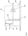
- FIG. 1 shows a Bockschatsent a circuit device according to the invention, with the electronic modules can be protected against overvoltages, which can possibly couple via their supply voltage inputs.
- the electronic modules in the automation and safety technology are usually designed for a rated voltage of 24 VDC, with one supply voltage range between 18 VDC and 32 VDC (including ripples and all tolerances) is usually allowed.
- the in the FIG. 1 shown circuit device has on the input side two voltage terminals 1 and 3, to which a power supply device can be connected. For example, a nominal voltage of 24 VDC can be provided between these voltage terminals, with the voltage terminal 3 leading to the reference potential (GND).
- the circuit device again comprises two further voltage terminals 2 and 4, to which a respective electronic module to be protected against overvoltages can be connected.
- the voltage terminal 4 is connected by way of example to the input-side reference potential terminal 3, while the output voltage terminal 2 in the example shown can be separated from the voltage at the input voltage terminal 1 via two series-connected switching devices 30 and 31.
- the circuit device according to the invention can both be a component of an electronic module, as well as be used in a separate overvoltage module, to which an electronic module can be connected.
- the circuit device can of course also be realized with a single-channel disconnectable supply path between the voltage terminals 1 and 2.
- the switching devices 30, 31 may also be bipolar, so that both the voltage terminal 1, and the reference potential terminal 3 is switchably connected to the associated voltage terminals 2 and 4 at the output.
- the switching devices 30 and 31 are in the FIG. 1 exemplified as a relay, which in principle also semiconductor switches are used, which preferably have a galvanic isolation to the control device 50.
- the switching devices 30 and 31 are each controlled redundantly via a separate control channel by a control device 50.
- the control device 50 is connected to a measuring circuit 40, with which a supply voltage applied between the input-side voltage terminals 1 and 3 can be detected, measured and / or monitored.
- the power supply for the control device 50 is provided indirectly via the input-side voltage terminals 1 and 3, wherein the control device 50 is arranged behind a voltage converter 60.
- Input side is the voltage converter 60 is designed for DC and AC voltages in a wide voltage range, for example, up to 120 V, so that the output side of a regulated, that is independent of the wide input voltage range operating voltage for the control device 50 is ready.
- the control device 50 for monitoring the voltage applied to the circuit device supply voltage is thus against overvoltages, i. against voltages exceeding the allowable voltages, e.g. 32 VDC, go out, protected behind the voltage converter 60 arranged.
- the voltage transformer With a maximum input voltage of e.g. 120 V, the voltage transformer is much more voltage-resistant than the connectable to the terminals 2 and 4 electronic modules to be protected by the circuit device.
- the control device 50 controls the switching devices 30 and 31 via an internal logic, which can be provided by a microcontroller, for example, such that the output voltage connection 2 is disconnected from the voltage connection 1 when an overvoltage is detected, before a downstream and protected against overvoltage 24 V module is endangered or destroyed.
- the switching characteristics of the switching devices 30 and 31, like the voltage converter 60 also, are limited to a maximum expected overvoltage, e.g. 120 V, and designed a corresponding maximum current.
- the control device 50 is connected to the measuring circuit 40 via a number of lines 5 for controlling, measuring or signaling, so that in cooperation of these two components, the voltage between the voltage terminal 1 and the reference potential terminal 3 can be evaluated.
- the measuring circuit 40 is also suitable in particular for detecting high-resistance overvoltages.
- the lines 5 are in the Figures 2 . 3 . 4 . 5 and 6 Nos. 521 to 523, 531 to 533, 541 to 544, 551 to 554 and 561 to 568, respectively.
- the measuring circuit 40 is cyclically tested by the control device 50 via the lines 5 for their functionality.
- a reliable separation of the downstream electronic modules is guaranteed by an overvoltage at any time. If a malfunction in the measuring circuit 40 is detected, the output voltage terminal 2 is disconnected from the input voltage connection via the switching devices 30 and 31, respectively. An error detected by the control device 50 can thus be signaled at least by switching off a downstream electronic module.
- the logic of the control device 50 can be implemented as one or more channels in order to control a corresponding number of switching devices in a redundant manner.
- a plurality of parallel measuring circuits 40 for monitoring the supply voltage can be provided in order to further increase the redundancy and safety of the circuit device.
- safe logic inputs 51 and logic outputs 52 can be provided on the control device 50, with which enable safety functions such as EMERGENCY STOP applications.
- the measuring circuit 40 for monitoring the input voltage can, as will become apparent in the following figures, be carried out with or without a galvanic isolation between the control device 50 and the voltage connections 1 and 3 as required.
- the measuring circuit 40 may include a testable level detecting circuit 42, 44, 45 or 46 or a voltage measuring device 43.
- a first level detection circuit 42 is shown, which is usable as a measuring circuit 40. With this circuit, an overvoltage between the two voltage terminals 1 and 3 can be seen.
- the circuit comprises a voltage divider having a first resistor 420 and a second resistor 421, a reference voltage source 422 and a comparator 423.
- the non-inverting input of the comparator is connected to the voltage divider, at the inverting input is the reference voltage of the reference voltage source 422.
- the voltage divider is dimensioned such that when an overvoltage occurs between the voltage terminals 1 and 3, a voltage at the non-inverting input of the comparator that is greater than the reference voltage U Ref provided by the reference voltage source 422 drops. In this case, a signal is sent to the control device 50 via a signal line 522 at the output of the comparator 423.
- the voltage divider is preferably designed with high resistance in order to avoid overloading of the voltage supply device at the voltage terminals 1 and 3, in particular in the case of overvoltage.
- the level detection circuit 42 further comprises a controllable by the controller 50 transistor 424, which is used for testing the overvoltage detection.
- the transistor 424 is connected in parallel with the first resistor 420, with which the voltage divider is tunable such that the voltage at the non-inverting input of the comparator 423 exceeds the reference voltage within a permissible supply voltage.
- the transistor 424 can be actuated by the control device 50 via the control line 521 within a test cycle. If the level detection circuit 42 is operating properly, a corresponding response or feedback signal from the comparator 423 is received from the controller 50 via the measurement line 522.
- another resistor may be connected in series with the transistor 424.
- the FIG. 3 shows a voltage measuring device 43, which is an alternative to the level switch 42.
- the voltage applied to the input-side voltage terminals 1 and 3 supply voltage can be measured.
- the supply voltage value divided by the voltage divider is digitized by the analog-to-digital converter 432 and transmitted to the logic of the controller 50 via a parallel or serial connection 532.
- the digitized voltage value is compared with a limit value, so that an overvoltage between the voltage terminals 1 and 3 in the logic of the control device 50 is detected.
- the voltage divider With the transistor 433, which is connected in parallel with the first resistor 430, the voltage divider can be detuned such that the control device 50 can infer from the change in the sampled voltage value to the functional capability or to a malfunction in the voltage measuring device 43.
- the transistor 433 may alternatively be arranged parallel to the second resistor 431 in order to detune the voltage divider in a suitable manner.
- FIG. 4 An alternative level detection circuit 44 for detecting an overvoltage is shown in FIG. 4 shown. This includes, like the previously described level detection circuit 41, a voltage divider with the resistors 440 and 441. A comparison circuit is formed by the transistor 443 with the collector resistor 442 and the emitter resistor 444.
- the voltage divider is dimensioned, for example, such that when exceeding a maximum permissible supply voltage of 32 V, the forward voltage at the base-emitter junction is exceeded.
- the transistor switches through, so that a corresponding level change on the line 543 signals an overvoltage to the control device 50.
- the measuring circuit 44 can be cyclically tested by the controlled change of the divider ratio.
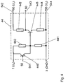
- FIGS 5 and 6 show two preferred embodiments of a level detection circuit 45 and 46, which has a complete electrical isolation to the control device 50 and is characterized by a structurally efficient structure.
- the testable level detection circuit 45 included in the FIG. 5 provides a preferably high-impedance measuring path, which is arranged parallel to the switchable main current path of the circuit device.
- the measuring path between the input-side voltage terminals 1 and 3 comprises a Zener diode 452 and a voltage divider comprising at least two resistors 450 and 451.
- Connected in parallel with the second resistor 451 is the light-emitting diode 4531 of a first optocoupler 453.
- the Zener diode has a Z voltage of 30 V.
- the Z-diode blocks, so that no current flows through the measuring path. Thus, no measurable event occurs.
- the switching threshold of the optocoupler 453 When the maximum supply voltage of 32 V is exceeded, the switching threshold of the optocoupler 453 is thus reached, so that the overvoltage is transmitted to the control device 50 via the phototransistor 4532 and the signal lines 553 and 554. With the phototransistor 4542 of the second optocoupler 454, the Zener diode 452 for testing the level switch 45 can be bridged.
- the light-emitting diode 4541 in the input of the second optocoupler 454 is controlled by the control device 50 via the control lines 551 and 552.
- the measuring path with the bypassing of the Zener diode also becomes conductive in the nominal voltage range, so that a resulting voltage drop across the first resistor 450 exceeds the value of the forward voltage of the light-emitting diode 4531 of the first optocoupler.
- the controller 50 then receives an expected signal from the first optocoupler, as long as the illustrated level detection circuit 45 is functional.
- the in the FIG. 5 shown level detection circuit 45 is characterized as already mentioned in particular by a complete galvanic isolation between the measuring path and the control device 50 from. Another essential advantage of this circuit is that the threshold detection for detecting an overvoltage is provided by a circuit-related interaction of Zener diode 452, the voltage divider 450 and 451 and the light emitting diode 4531 of the optocoupler 453. An additional comparator circuit including a possibly necessary power supply is not required.
- FIG. 6 an alternative embodiment of a two-channel level detection circuit 46 is shown, which also has a complete galvanic isolation to the control device 50.
- the two-channel testable level detection circuit 46 provides a preferably high-impedance sense current path which is arranged in parallel with the switchable main current path of the circuit device.
- This measuring current path comprises a first and a second measuring channel, each channel having a respective Zener diode 4612 or 4622 and a voltage divider comprising a first resistor 4610 or 4620 and a second resistor 4611 or 4621.
- a light-emitting diode 4631 or 4641 of a first optocoupler 463 or 464 is connected in parallel in each case.
- the light-emitting diode has in each case a forward voltage of, for example, 1.1 V.
- the Z-diodes 4612 and 4622 of both measuring channels each have a Z voltage of, for example, 14 V.
- the two measuring channels can each be bridged via a switchable transistor of a second optocoupler 465 or 466 for testing the level detection circuit 46.
- a measuring path can also have more than the two measuring channels shown, wherein the dimensioning of the Z-diodes must be adjusted according to the number of channels.
- the measurement path of the level detection circuit 46 When the supply voltage applied to the two voltage terminals 1 and 3 is in the range of the rated voltage of 24 VDC, no current flows through the measurement path of the level detection circuit 46. If the supply voltage exceeds the sum of the Z voltages of both Zener diodes 4612 and 4622, i. for example, a value of 28 V, the measurement path becomes conductive.
- the measuring path is particularly in view of large overvoltages e.g. of up to 120 V high impedance designed to limit the flow of current and the thermal load and to ensure a corresponding dielectric strength.
- a resistor 467 may also be provided at the output of the measuring current path.
- the illustrated resistor network is dimensioned such that at the latest when reaching the maximum allowable supply voltage of 32 V, the optocouplers 463 and 464, i. their integrated LEDs 4631 and 4641 are turned on. Via the signal line pairs 563, 564 and 567 and 568, an overvoltage situation can be signaled to the control device 50 in two channels.
- the two exemplary measurement channels each include a second optocoupler 465 and 466, which enable testability of the level detection circuit 46.
- a Triggered test signal from the controller 50, one of the two optocouplers is activated in each case, so that the corresponding measuring channel is bridged.
- a supply voltage in the range of the nominal voltage of 24 V exceeds the Z voltage of the Zener diode of the remaining, ie not bridged, measuring channel, so that it switches through.
- the forward voltage of the respective light emitting diode in the optocoupler of the remaining measuring channel is also exceeded, so that the optocoupler is activated.
- the control device 50 receives, assuming a functioning level detection circuit 46, in each case a feedback signal via the respective non-bridged measuring channel.
- the measurement channels are cyclically alternately tested. If a feedback signal to a transmitted test signal, the controller 50 may indicate a malfunction within the level detection circuit 46.
Landscapes
- Emergency Protection Circuit Devices (AREA)
- Protection Of Static Devices (AREA)
- Dc-Dc Converters (AREA)
Claims (14)
- Dispositif de commutation pour la protection de groupes de composants électroniques contre les surtensions, comportant une entrée de tension (1) et une sortie de tension (2) reliées l'une à l'autre de manière commutable par au moins une unité de commutation (30), comprenant en outre un circuit de mesure (40) pour la détection d'une tension à l'entrée de tension (1) et un dispositif de commande (50), ledit dispositif de commande (50) étant réalisé pour commander l'unité de commutation (30) en fonction de la tension détectée par le circuit de mesure (40) de manière à séparer la sortie de tension (2) de l'entrée de tension (1) au moyen de l'unité de commutation (30) en cas de surtension à l'entrée de tension (1), le dispositif de commande (50) étant relié à l'entrée de tension (1) par un transformateur de tension (60) de manière à assurer une alimentation en tension pour le dispositif de commande (50) y compris en cas de surtension, caractérisé en ce que l'aptitude au fonctionnement du circuit de mesure (40) peut être cycliquement testée par un transistor (424 ; 433 ; 445 ; 4542 ; 4652, 4662) commandé par le dispositif de commande (50).
- Dispositif de commutation selon la revendication précédente, caractérisé en ce que le circuit de mesure (40) présente un chemin de courant de mesure avec au moins un canal de mesure, un interrupteur de niveau (423, 443, 453, 463, 464) étant associé à chaque canal de mesure.
- Dispositif de commutation selon la revendication précédente, caractérisé en ce que les interrupteurs de niveau sont prévus pour détecter le dépassement d'un niveau de tension prédéfini et à signaler celui-ci au dispositif de commande (50) via une ligne de signaux (5).
- Dispositif de commutation selon la revendication précédente, caractérisé en ce qu'un élément de commutation (424 ; 445 ; 4542 ; 4652, 4662) est associé à chaque canal de mesure, lequel est commandé par le dispositif de commande (50) et est prévu pour tester le circuit de mesure (40).
- Dispositif de commutation selon la revendication 4, caractérisé en ce que l'interrupteur de niveau comprend un comparateur (423) relié à une source de tension de référence (422).
- Dispositif de commutation selon la revendication 4, caractérisé en ce que l'interrupteur de niveau comprend un transistor (443).
- Dispositif de commutation selon la revendication 4, caractérisé en ce que l'interrupteur de niveau comprend un premier optocoupleur (453 ; 463, 464) et l'élément de commutation un deuxième optocoupleur (454 ; 465, 466).
- Dispositif de commutation selon la revendication 7, caractérisé en ce que le chemin de courant de mesure comporte un canal de mesure comprenant un circuit en série composé d'une diode Zener (452), d'une première résistance (450) et d'une deuxième résistance (451), le premier optocoupleur (453) étant monté parallèlement à la deuxième résistance (451).
- Dispositif de commutation selon la revendication 7 ou 8, caractérisé en ce que le deuxième optocoupleur (454) est monté parallèlement à la diode Zener (452), si bien que la diode peut être pontée pour le test du circuit de mesure (40).
- Dispositif de commutation selon la revendication 7, caractérisé en ce que le chemin de courant de mesure comprend au moins deux canaux de mesure montés en série, chaque canal de mesure comprenant un circuit en série composé d'une diode Zener (4612, 4622), d'une première résistance (4610, 4620) et d'une deuxième résistance (4611, 4621), le premier optocoupleur (463, 464) d'un canal de mesure étant monté en parallèle à la deuxième résistance.
- Dispositif de commutation selon la revendication 7, caractérisé en ce que le deuxième optocoupleur (465, 466) est monté en parallèle au canal de mesure associé, si bien que chaque canal de mesure peut être ponté pour le test du circuit de mesure (40).
- Dispositif de commutation selon la revendication 1, caractérisé en ce que le circuit de mesure (40 ; 43) comprend un diviseur de tension (430, 431) et un convertisseur analogique/numérique (432) pour la mesure et la numérisation d'une tension à l'entrée de tension (1).
- Module électronique de protection contre les surtensions comprenant un dispositif de commutation selon l'une des revendication 1 à 12, caractérisé en ce que la sortie de tension (2) du dispositif de commutation peut être reliée à un groupe de composants électroniques, et en ce que l'entrée de tension (1) peut être reliée à une source de tension.
- Utilisation d'un dispositif de commutation selon l'une des revendications 1 à 12 à l'intérieur d'un groupe de composants électroniques.
Applications Claiming Priority (2)
| Application Number | Priority Date | Filing Date | Title |
|---|---|---|---|
| DE102011115852 | 2011-10-13 | ||
| DE102012004577.8A DE102012004577B4 (de) | 2011-10-13 | 2012-03-09 | Schaltungsvorrichtung für einen Überspannungsschutz elektronischer Baugruppen, Überspannungsschutzmodul mit der Schaltungsvorrichtung und Verwendung der Schaltungsvorrichtung |
Publications (2)
| Publication Number | Publication Date |
|---|---|
| EP2582001A1 EP2582001A1 (fr) | 2013-04-17 |
| EP2582001B1 true EP2582001B1 (fr) | 2016-11-02 |
Family
ID=46798946
Family Applications (1)
| Application Number | Title | Priority Date | Filing Date |
|---|---|---|---|
| EP12005573.6A Active EP2582001B1 (fr) | 2011-10-13 | 2012-07-31 | Dispositif de protection contre les surtensions pour modules électroniques |
Country Status (1)
| Country | Link |
|---|---|
| EP (1) | EP2582001B1 (fr) |
Families Citing this family (1)
| Publication number | Priority date | Publication date | Assignee | Title |
|---|---|---|---|---|
| DE102018207503A1 (de) * | 2018-05-15 | 2019-11-21 | Continental Teves Ag & Co. Ohg | Schaltungsanordnung zum Schutz einer elektronischen Baugruppe |
Family Cites Families (6)
| Publication number | Priority date | Publication date | Assignee | Title |
|---|---|---|---|---|
| DE3923710A1 (de) * | 1989-07-18 | 1991-01-24 | Philips Patentverwaltung | Stromversorgungseinrichtung mit gleichspannungsueberwachungsschaltung |
| US20040184208A1 (en) * | 2003-03-19 | 2004-09-23 | Daniel Liu | Power protecting device for electrical power source and load |
| TWM313812U (en) * | 2006-11-27 | 2007-06-11 | Micro Star Int Co Ltd | Computer device with over voltage protection |
| DE102008051514B4 (de) * | 2008-10-14 | 2022-08-25 | Robert Bosch Gmbh | Spannungsüberwachungsanordnung für ein Sicherheitsmodul |
| US8203815B2 (en) * | 2009-05-08 | 2012-06-19 | Hamilton Sundstrand Corporation | System and method to provide transient overvoltage suppression |
| TW201145742A (en) * | 2010-06-03 | 2011-12-16 | Hon Hai Prec Ind Co Ltd | Power supply protecting apparatus |
-
2012
- 2012-07-31 EP EP12005573.6A patent/EP2582001B1/fr active Active
Also Published As
| Publication number | Publication date |
|---|---|
| EP2582001A1 (fr) | 2013-04-17 |
Similar Documents
| Publication | Publication Date | Title |
|---|---|---|
| EP2817860B1 (fr) | Dispositif de commutation de sécurité avec bloc d'alimentation | |
| EP2951901B1 (fr) | Dispositif de commutation de sécurité à alimentation sécurisée | |
| EP2104974B1 (fr) | Dispositif de protection contre les surtensions pour un appareil électronique | |
| EP3449478B1 (fr) | Module de fourniture d'une puissance de sortie électrique à sécurité intrinsèque ainsi que dispositif d'éclairage protégé contre les explosions | |
| DE102015211510A1 (de) | Relaisüberwachung | |
| EP3451476A1 (fr) | Procédé et circuit permettant la conformité aux valeurs maximales pour paramètres de sortie d'une alimentation électrique | |
| DE102015000576A1 (de) | Kraftfahrzeug mit Schaltvorrichtung für eine bordnetzbetriebene Komponente | |
| DE4436858C2 (de) | Überspannungsschutzeinrichtung | |
| EP2582001B1 (fr) | Dispositif de protection contre les surtensions pour modules électroniques | |
| WO2002071600A2 (fr) | Dispositif de commutation de securite | |
| DE102018118647A1 (de) | Einzelfehlersichere elektronische Sicherheitsschaltung | |
| DE102012004577B4 (de) | Schaltungsvorrichtung für einen Überspannungsschutz elektronischer Baugruppen, Überspannungsschutzmodul mit der Schaltungsvorrichtung und Verwendung der Schaltungsvorrichtung | |
| DE102014011717B4 (de) | Verfahren und Vorrichtung zur eigensicheren, redundanten Stromversorgung von Feldgeräten | |
| DE102020210554A1 (de) | Wechselrichter | |
| DE102014011723B4 (de) | Vorrichtung zur eigensicheren, redundanten Stromversorgung von Feldgeräten | |
| DE102012016696A1 (de) | Schaltungsanordnung und Verfahren zur Gleichstromunterbrechung | |
| DE102017126754B4 (de) | Eingangsschaltung zum fehlersicheren Einlesen eines analogen Eingangssignals | |
| DE102019124213A1 (de) | Galvanisch verbundenes AC-Ladegerät mit Überwachungs- und Diagnosesystem | |
| DE102012222782A1 (de) | Schaltvorrichtung mit Überspannungsschutz | |
| DE102008029679B4 (de) | System, Verfahren und elektronische Schaltung für mindestens eine elektronische Schaltungseinheit | |
| EP2580854B1 (fr) | Convertisseur doté d'un dispositif de surveillance de commutateur | |
| DE102014100830A1 (de) | Elektrische Sicherung, dezentrale Sicherungseinheit sowie System | |
| DE102015220268A1 (de) | Vorrichtung und Verfahren zum Erkennen einer Fehlfunktion in einem Halbleiterschaltmodul | |
| DD282300A5 (de) | Schaltung zum ueberwachen des betriebsstromes in stromkreisen von einphasenwechselstrom-elektroenergieverbrauchern | |
| DD282299A5 (de) | Schaltung zum ueberwachen des betriebsstromes in stromkreisen von gleichstrom-elektroenergieverbrauchern |
Legal Events
| Date | Code | Title | Description |
|---|---|---|---|
| PUAI | Public reference made under article 153(3) epc to a published international application that has entered the european phase |
Free format text: ORIGINAL CODE: 0009012 |
|
| AK | Designated contracting states |
Kind code of ref document: A1 Designated state(s): AL AT BE BG CH CY CZ DE DK EE ES FI FR GB GR HR HU IE IS IT LI LT LU LV MC MK MT NL NO PL PT RO RS SE SI SK SM TR |
|
| AX | Request for extension of the european patent |
Extension state: BA ME |
|
| 17P | Request for examination filed |
Effective date: 20130927 |
|
| RBV | Designated contracting states (corrected) |
Designated state(s): AL AT BE BG CH CY CZ DE DK EE ES FI FR GB GR HR HU IE IS IT LI LT LU LV MC MK MT NL NO PL PT RO RS SE SI SK SM TR |
|
| 17Q | First examination report despatched |
Effective date: 20141212 |
|
| REG | Reference to a national code |
Ref country code: DE Ref legal event code: R079 Ref document number: 502012008648 Country of ref document: DE Free format text: PREVIOUS MAIN CLASS: H02H0003200000 Ipc: H02H0001060000 |
|
| GRAP | Despatch of communication of intention to grant a patent |
Free format text: ORIGINAL CODE: EPIDOSNIGR1 |
|
| RIC1 | Information provided on ipc code assigned before grant |
Ipc: H02H 1/06 20060101AFI20160511BHEP Ipc: H02H 3/20 20060101ALI20160511BHEP |
|
| INTG | Intention to grant announced |
Effective date: 20160601 |
|
| GRAS | Grant fee paid |
Free format text: ORIGINAL CODE: EPIDOSNIGR3 |
|
| GRAA | (expected) grant |
Free format text: ORIGINAL CODE: 0009210 |
|
| AK | Designated contracting states |
Kind code of ref document: B1 Designated state(s): AL AT BE BG CH CY CZ DE DK EE ES FI FR GB GR HR HU IE IS IT LI LT LU LV MC MK MT NL NO PL PT RO RS SE SI SK SM TR |
|
| REG | Reference to a national code |
Ref country code: GB Ref legal event code: FG4D Free format text: NOT ENGLISH |
|
| REG | Reference to a national code |
Ref country code: AT Ref legal event code: REF Ref document number: 842706 Country of ref document: AT Kind code of ref document: T Effective date: 20161115 Ref country code: CH Ref legal event code: EP |
|
| REG | Reference to a national code |
Ref country code: IE Ref legal event code: FG4D Free format text: LANGUAGE OF EP DOCUMENT: GERMAN |
|
| REG | Reference to a national code |
Ref country code: DE Ref legal event code: R096 Ref document number: 502012008648 Country of ref document: DE |
|
| PG25 | Lapsed in a contracting state [announced via postgrant information from national office to epo] |
Ref country code: LV Free format text: LAPSE BECAUSE OF FAILURE TO SUBMIT A TRANSLATION OF THE DESCRIPTION OR TO PAY THE FEE WITHIN THE PRESCRIBED TIME-LIMIT Effective date: 20161102 |
|
| REG | Reference to a national code |
Ref country code: NL Ref legal event code: MP Effective date: 20161102 |
|
| REG | Reference to a national code |
Ref country code: LT Ref legal event code: MG4D |
|
| PG25 | Lapsed in a contracting state [announced via postgrant information from national office to epo] |
Ref country code: NO Free format text: LAPSE BECAUSE OF FAILURE TO SUBMIT A TRANSLATION OF THE DESCRIPTION OR TO PAY THE FEE WITHIN THE PRESCRIBED TIME-LIMIT Effective date: 20170202 Ref country code: GR Free format text: LAPSE BECAUSE OF FAILURE TO SUBMIT A TRANSLATION OF THE DESCRIPTION OR TO PAY THE FEE WITHIN THE PRESCRIBED TIME-LIMIT Effective date: 20170203 Ref country code: SE Free format text: LAPSE BECAUSE OF FAILURE TO SUBMIT A TRANSLATION OF THE DESCRIPTION OR TO PAY THE FEE WITHIN THE PRESCRIBED TIME-LIMIT Effective date: 20161102 Ref country code: NL Free format text: LAPSE BECAUSE OF FAILURE TO SUBMIT A TRANSLATION OF THE DESCRIPTION OR TO PAY THE FEE WITHIN THE PRESCRIBED TIME-LIMIT Effective date: 20161102 Ref country code: LT Free format text: LAPSE BECAUSE OF FAILURE TO SUBMIT A TRANSLATION OF THE DESCRIPTION OR TO PAY THE FEE WITHIN THE PRESCRIBED TIME-LIMIT Effective date: 20161102 |
|
| PG25 | Lapsed in a contracting state [announced via postgrant information from national office to epo] |
Ref country code: PL Free format text: LAPSE BECAUSE OF FAILURE TO SUBMIT A TRANSLATION OF THE DESCRIPTION OR TO PAY THE FEE WITHIN THE PRESCRIBED TIME-LIMIT Effective date: 20161102 Ref country code: IS Free format text: LAPSE BECAUSE OF FAILURE TO SUBMIT A TRANSLATION OF THE DESCRIPTION OR TO PAY THE FEE WITHIN THE PRESCRIBED TIME-LIMIT Effective date: 20170302 Ref country code: PT Free format text: LAPSE BECAUSE OF FAILURE TO SUBMIT A TRANSLATION OF THE DESCRIPTION OR TO PAY THE FEE WITHIN THE PRESCRIBED TIME-LIMIT Effective date: 20170302 Ref country code: HR Free format text: LAPSE BECAUSE OF FAILURE TO SUBMIT A TRANSLATION OF THE DESCRIPTION OR TO PAY THE FEE WITHIN THE PRESCRIBED TIME-LIMIT Effective date: 20161102 Ref country code: ES Free format text: LAPSE BECAUSE OF FAILURE TO SUBMIT A TRANSLATION OF THE DESCRIPTION OR TO PAY THE FEE WITHIN THE PRESCRIBED TIME-LIMIT Effective date: 20161102 Ref country code: RS Free format text: LAPSE BECAUSE OF FAILURE TO SUBMIT A TRANSLATION OF THE DESCRIPTION OR TO PAY THE FEE WITHIN THE PRESCRIBED TIME-LIMIT Effective date: 20161102 Ref country code: FI Free format text: LAPSE BECAUSE OF FAILURE TO SUBMIT A TRANSLATION OF THE DESCRIPTION OR TO PAY THE FEE WITHIN THE PRESCRIBED TIME-LIMIT Effective date: 20161102 |
|
| REG | Reference to a national code |
Ref country code: FR Ref legal event code: PLFP Year of fee payment: 6 |
|
| PG25 | Lapsed in a contracting state [announced via postgrant information from national office to epo] |
Ref country code: RO Free format text: LAPSE BECAUSE OF FAILURE TO SUBMIT A TRANSLATION OF THE DESCRIPTION OR TO PAY THE FEE WITHIN THE PRESCRIBED TIME-LIMIT Effective date: 20161102 Ref country code: EE Free format text: LAPSE BECAUSE OF FAILURE TO SUBMIT A TRANSLATION OF THE DESCRIPTION OR TO PAY THE FEE WITHIN THE PRESCRIBED TIME-LIMIT Effective date: 20161102 Ref country code: CZ Free format text: LAPSE BECAUSE OF FAILURE TO SUBMIT A TRANSLATION OF THE DESCRIPTION OR TO PAY THE FEE WITHIN THE PRESCRIBED TIME-LIMIT Effective date: 20161102 Ref country code: DK Free format text: LAPSE BECAUSE OF FAILURE TO SUBMIT A TRANSLATION OF THE DESCRIPTION OR TO PAY THE FEE WITHIN THE PRESCRIBED TIME-LIMIT Effective date: 20161102 Ref country code: SK Free format text: LAPSE BECAUSE OF FAILURE TO SUBMIT A TRANSLATION OF THE DESCRIPTION OR TO PAY THE FEE WITHIN THE PRESCRIBED TIME-LIMIT Effective date: 20161102 |
|
| REG | Reference to a national code |
Ref country code: DE Ref legal event code: R097 Ref document number: 502012008648 Country of ref document: DE |
|
| PG25 | Lapsed in a contracting state [announced via postgrant information from national office to epo] |
Ref country code: SM Free format text: LAPSE BECAUSE OF FAILURE TO SUBMIT A TRANSLATION OF THE DESCRIPTION OR TO PAY THE FEE WITHIN THE PRESCRIBED TIME-LIMIT Effective date: 20161102 Ref country code: BG Free format text: LAPSE BECAUSE OF FAILURE TO SUBMIT A TRANSLATION OF THE DESCRIPTION OR TO PAY THE FEE WITHIN THE PRESCRIBED TIME-LIMIT Effective date: 20170202 |
|
| PLBE | No opposition filed within time limit |
Free format text: ORIGINAL CODE: 0009261 |
|
| STAA | Information on the status of an ep patent application or granted ep patent |
Free format text: STATUS: NO OPPOSITION FILED WITHIN TIME LIMIT |
|
| 26N | No opposition filed |
Effective date: 20170803 |
|
| PG25 | Lapsed in a contracting state [announced via postgrant information from national office to epo] |
Ref country code: SI Free format text: LAPSE BECAUSE OF FAILURE TO SUBMIT A TRANSLATION OF THE DESCRIPTION OR TO PAY THE FEE WITHIN THE PRESCRIBED TIME-LIMIT Effective date: 20161102 |
|
| REG | Reference to a national code |
Ref country code: CH Ref legal event code: PL |
|
| GBPC | Gb: european patent ceased through non-payment of renewal fee |
Effective date: 20170731 |
|
| PG25 | Lapsed in a contracting state [announced via postgrant information from national office to epo] |
Ref country code: CH Free format text: LAPSE BECAUSE OF NON-PAYMENT OF DUE FEES Effective date: 20170731 Ref country code: GB Free format text: LAPSE BECAUSE OF NON-PAYMENT OF DUE FEES Effective date: 20170731 Ref country code: LI Free format text: LAPSE BECAUSE OF NON-PAYMENT OF DUE FEES Effective date: 20170731 |
|
| REG | Reference to a national code |
Ref country code: IE Ref legal event code: MM4A |
|
| REG | Reference to a national code |
Ref country code: BE Ref legal event code: MM Effective date: 20170731 |
|
| PG25 | Lapsed in a contracting state [announced via postgrant information from national office to epo] |
Ref country code: LU Free format text: LAPSE BECAUSE OF NON-PAYMENT OF DUE FEES Effective date: 20170731 |
|
| REG | Reference to a national code |
Ref country code: FR Ref legal event code: PLFP Year of fee payment: 7 |
|
| PG25 | Lapsed in a contracting state [announced via postgrant information from national office to epo] |
Ref country code: IE Free format text: LAPSE BECAUSE OF NON-PAYMENT OF DUE FEES Effective date: 20170731 |
|
| PG25 | Lapsed in a contracting state [announced via postgrant information from national office to epo] |
Ref country code: BE Free format text: LAPSE BECAUSE OF NON-PAYMENT OF DUE FEES Effective date: 20170731 |
|
| REG | Reference to a national code |
Ref country code: AT Ref legal event code: MM01 Ref document number: 842706 Country of ref document: AT Kind code of ref document: T Effective date: 20170731 |
|
| PG25 | Lapsed in a contracting state [announced via postgrant information from national office to epo] |
Ref country code: MT Free format text: LAPSE BECAUSE OF FAILURE TO SUBMIT A TRANSLATION OF THE DESCRIPTION OR TO PAY THE FEE WITHIN THE PRESCRIBED TIME-LIMIT Effective date: 20161102 |
|
| PG25 | Lapsed in a contracting state [announced via postgrant information from national office to epo] |
Ref country code: AT Free format text: LAPSE BECAUSE OF NON-PAYMENT OF DUE FEES Effective date: 20170731 |
|
| PG25 | Lapsed in a contracting state [announced via postgrant information from national office to epo] |
Ref country code: MC Free format text: LAPSE BECAUSE OF FAILURE TO SUBMIT A TRANSLATION OF THE DESCRIPTION OR TO PAY THE FEE WITHIN THE PRESCRIBED TIME-LIMIT Effective date: 20161102 Ref country code: HU Free format text: LAPSE BECAUSE OF FAILURE TO SUBMIT A TRANSLATION OF THE DESCRIPTION OR TO PAY THE FEE WITHIN THE PRESCRIBED TIME-LIMIT; INVALID AB INITIO Effective date: 20120731 |
|
| PG25 | Lapsed in a contracting state [announced via postgrant information from national office to epo] |
Ref country code: CY Free format text: LAPSE BECAUSE OF NON-PAYMENT OF DUE FEES Effective date: 20161102 |
|
| PG25 | Lapsed in a contracting state [announced via postgrant information from national office to epo] |
Ref country code: MK Free format text: LAPSE BECAUSE OF FAILURE TO SUBMIT A TRANSLATION OF THE DESCRIPTION OR TO PAY THE FEE WITHIN THE PRESCRIBED TIME-LIMIT Effective date: 20161102 |
|
| PG25 | Lapsed in a contracting state [announced via postgrant information from national office to epo] |
Ref country code: TR Free format text: LAPSE BECAUSE OF FAILURE TO SUBMIT A TRANSLATION OF THE DESCRIPTION OR TO PAY THE FEE WITHIN THE PRESCRIBED TIME-LIMIT Effective date: 20161102 |
|
| PG25 | Lapsed in a contracting state [announced via postgrant information from national office to epo] |
Ref country code: AL Free format text: LAPSE BECAUSE OF FAILURE TO SUBMIT A TRANSLATION OF THE DESCRIPTION OR TO PAY THE FEE WITHIN THE PRESCRIBED TIME-LIMIT Effective date: 20161102 |
|
| P01 | Opt-out of the competence of the unified patent court (upc) registered |
Effective date: 20230424 |
|
| PGFP | Annual fee paid to national office [announced via postgrant information from national office to epo] |
Ref country code: IT Payment date: 20230721 Year of fee payment: 12 |
|
| PGFP | Annual fee paid to national office [announced via postgrant information from national office to epo] |
Ref country code: FR Payment date: 20230725 Year of fee payment: 12 Ref country code: DE Payment date: 20230928 Year of fee payment: 12 |