EP2582001B1 - Excess voltage protective device for electronic modules - Google Patents
Excess voltage protective device for electronic modules Download PDFInfo
- Publication number
- EP2582001B1 EP2582001B1 EP12005573.6A EP12005573A EP2582001B1 EP 2582001 B1 EP2582001 B1 EP 2582001B1 EP 12005573 A EP12005573 A EP 12005573A EP 2582001 B1 EP2582001 B1 EP 2582001B1
- Authority
- EP
- European Patent Office
- Prior art keywords
- voltage
- measuring
- circuit device
- control device
- circuit
- Prior art date
- Legal status (The legal status is an assumption and is not a legal conclusion. Google has not performed a legal analysis and makes no representation as to the accuracy of the status listed.)
- Active
Links
Images


Classifications
-
- H—ELECTRICITY
- H02—GENERATION; CONVERSION OR DISTRIBUTION OF ELECTRIC POWER
- H02H—EMERGENCY PROTECTIVE CIRCUIT ARRANGEMENTS
- H02H3/00—Emergency protective circuit arrangements for automatic disconnection directly responsive to an undesired change from normal electric working condition with or without subsequent reconnection ; integrated protection
- H02H3/20—Emergency protective circuit arrangements for automatic disconnection directly responsive to an undesired change from normal electric working condition with or without subsequent reconnection ; integrated protection responsive to excess voltage
- H02H3/202—Emergency protective circuit arrangements for automatic disconnection directly responsive to an undesired change from normal electric working condition with or without subsequent reconnection ; integrated protection responsive to excess voltage for DC systems
-
- H—ELECTRICITY
- H02—GENERATION; CONVERSION OR DISTRIBUTION OF ELECTRIC POWER
- H02H—EMERGENCY PROTECTIVE CIRCUIT ARRANGEMENTS
- H02H1/00—Details of emergency protective circuit arrangements
- H02H1/06—Arrangements for supplying operative power
Definitions
- the present invention relates to a circuit device for overvoltage protection of electronic assemblies.
- suitable protection against overvoltages that can couple into an electronic module via the 24 VDC supply connections can, for example, be provided by a relay in the supply current path, with which a downstream electronic module to be protected can be disconnected from the supply connections as soon as possible Supply connections an overvoltage occurs.
- the relay picks up, so that a subsequent module is supplied with voltage.
- the quiescent current for switching on the relay is obtained via a circuit from the supply current path.
- Such a circuit may include, for example, a self-resetting fuse and an overvoltage protection diode that cooperatively form an overvoltage detector.
- the overvoltage protection diode is parallel to the relay coil arranged, wherein the response voltage of this diode is designed for the maximum allowable supply voltage.
- the fuse forms a series circuit together with the diode and the relay coil.
- the self-resetting fuse is triggered by the high current flowing through the switched-over overvoltage protection diode.
- the relay is disconnected from the supply and falls back to its rest position according to the quiescent current principle and interrupts the flow of current in the direction of the downstream electronic module.
- a disadvantage of the prior art is that for reliable triggering a sufficiently high current must flow through the fuse. A correspondingly high current flow requires a low-impedance character of the overvoltage. High-resistance overvoltages, on the other hand, can not be reliably detected, since a resistance within the supply circuit can limit the current for triggering the fuse such that the triggering threshold of the fuse is not exceeded.
- the US 2004/0184208 A1 discloses a protection device for monitoring an AC electric power supply.
- the DE 10 2008 051 514 A1 which forms the preamble of claim 1, discloses a voltage monitoring for safe operation of a security module with the possibility of power shutdown by an interruption means, which is verifiable by a further interruption means
- the DE 39 23 710 A1 discloses one
- Power supply device with monitoring circuit for at least two referenced to a common reference potential DC voltages of different polarity with a signal transmission element.
- the US 2008/0123236 A1 discloses a computer with an overvoltage protection device connected between a CPU of the computer and the power supply.
- the US 2010/0284114 A1 discloses a protection circuit for suppression of transient overvoltages.
- US 2011/0299205 A1 discloses a circuit protection circuit for over and under voltages.
- the invention has for its object to provide a device for overvoltage protection, with the high-voltage overvoltages can be reliably detected and turned off.
- the present invention proposes a circuit device for overvoltage protection of electronic assemblies comprising a voltage input and a voltage output, which are connected via at least one switching device switchable.
- the circuit device further comprises a measuring circuit for detecting a voltage at the voltage input and a control device.
- the control device is designed to control the switching device as a function of the voltage detected by the measuring circuit such that, in the event of an overvoltage at the voltage input, the voltage output is disconnected from the voltage input by means of the switching device.
- the control device is connected to the voltage input via a voltage converter such that a voltage supply for the control device is ensured even with an overvoltage.
- An essential advantage of a circuit device according to the present invention is that the control device is arranged behind a voltage converter which has a wide input voltage range.
- the maximum permissible input voltage range of the converter is a multiple of a maximum permissible supply voltage of an electronic module to be protected.
- the dielectric strength of the circuit device, ie the voltage range, by a surge protector reliable is ready is limited only by the input voltage range of the voltage converter up.
- the measuring circuit of a switching device may have a measuring current path with at least one measuring channel, wherein each measuring channel may preferably each have a level switch assigned to it.
- the level switches are preferably designed to detect the exceeding of a predetermined voltage level and to signal via an associated signal line to the control device.
- Each measuring channel may be assigned a switching element which can be controlled by the control device and which is designed to test the measuring circuit.
- the level switch may include, for example, a comparator connected to a reference voltage source.
- the level switch may comprise a transistor.
- the level switch may comprise a first optocoupler and the switching element may comprise a second optocoupler.
- the optocouplers allow a galvanic isolation between the measuring circuit and the controller connected thereto. Furthermore, the level switch is essentially formed by a light-emitting diode of the first optocoupler, so that an additional comparator is not required.
- the measuring current path may have a measuring channel which comprises a series connection of a Zener diode, a first resistor and a second resistor.
- the first optocoupler is preferably connected in parallel with the second resistor.
- the Zener diode is preferably switched in the reverse direction in the measurement channel, so that a predetermined voltage value must be exceeded for a current flow through the measurement path.
- the first and second resistors form a voltage divider which is dimensioned such that upon reaching an overvoltage at the light emitting diode, a forward voltage sufficient for switching through is applied.
- the second optocoupler is preferably connected in parallel with the Zener diode, so that the latter, by the control device, e.g. triggered by a test signal, for testing the measuring circuit can be bridged.
- the control device receives a resulting feedback signal on the transmitted test signal.
- the measuring current path may comprise a number of at least two measuring channels connected in series.
- Each measuring channel preferably comprises a series connection of a Zener diode, a first resistor and a second resistor.
- the first optocoupler of each measuring channel is preferably connected in parallel to the second resistor of the measuring channel.
- the second optocoupler can be connected in parallel to the assigned measuring channel, so that the respective measuring channel can be bridged for testing the measuring circuit.
- the measuring circuit may comprise a voltage divider and a digital / analog converter for measuring and digitizing a voltage at the voltage input.
- the controller may include means for comparing the digitized voltage value to an allowable limit.
- the invention also includes an overvoltage protection module comprising one of the previously described circuit devices suitable for connection to a downstream electronic subassembly. Such a module is particularly suitable for retrofitting an overvoltage protection for existing modules.
- the voltage output of the circuit device is preferably connectable to an input of an electronic module to be protected.
- the voltage input can be connected to a supply voltage source.
- the circuit device according to the invention can also be used as a component of an electronic module, which is preferably to be arranged directly at the entrance of such an assembly.
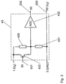
- FIG. 1 shows a Bockschatsent a circuit device according to the invention, with the electronic modules can be protected against overvoltages, which can possibly couple via their supply voltage inputs.
- the electronic modules in the automation and safety technology are usually designed for a rated voltage of 24 VDC, with one supply voltage range between 18 VDC and 32 VDC (including ripples and all tolerances) is usually allowed.
- the in the FIG. 1 shown circuit device has on the input side two voltage terminals 1 and 3, to which a power supply device can be connected. For example, a nominal voltage of 24 VDC can be provided between these voltage terminals, with the voltage terminal 3 leading to the reference potential (GND).
- the circuit device again comprises two further voltage terminals 2 and 4, to which a respective electronic module to be protected against overvoltages can be connected.
- the voltage terminal 4 is connected by way of example to the input-side reference potential terminal 3, while the output voltage terminal 2 in the example shown can be separated from the voltage at the input voltage terminal 1 via two series-connected switching devices 30 and 31.
- the circuit device according to the invention can both be a component of an electronic module, as well as be used in a separate overvoltage module, to which an electronic module can be connected.
- the circuit device can of course also be realized with a single-channel disconnectable supply path between the voltage terminals 1 and 2.
- the switching devices 30, 31 may also be bipolar, so that both the voltage terminal 1, and the reference potential terminal 3 is switchably connected to the associated voltage terminals 2 and 4 at the output.
- the switching devices 30 and 31 are in the FIG. 1 exemplified as a relay, which in principle also semiconductor switches are used, which preferably have a galvanic isolation to the control device 50.
- the switching devices 30 and 31 are each controlled redundantly via a separate control channel by a control device 50.
- the control device 50 is connected to a measuring circuit 40, with which a supply voltage applied between the input-side voltage terminals 1 and 3 can be detected, measured and / or monitored.
- the power supply for the control device 50 is provided indirectly via the input-side voltage terminals 1 and 3, wherein the control device 50 is arranged behind a voltage converter 60.
- Input side is the voltage converter 60 is designed for DC and AC voltages in a wide voltage range, for example, up to 120 V, so that the output side of a regulated, that is independent of the wide input voltage range operating voltage for the control device 50 is ready.
- the control device 50 for monitoring the voltage applied to the circuit device supply voltage is thus against overvoltages, i. against voltages exceeding the allowable voltages, e.g. 32 VDC, go out, protected behind the voltage converter 60 arranged.
- the voltage transformer With a maximum input voltage of e.g. 120 V, the voltage transformer is much more voltage-resistant than the connectable to the terminals 2 and 4 electronic modules to be protected by the circuit device.
- the control device 50 controls the switching devices 30 and 31 via an internal logic, which can be provided by a microcontroller, for example, such that the output voltage connection 2 is disconnected from the voltage connection 1 when an overvoltage is detected, before a downstream and protected against overvoltage 24 V module is endangered or destroyed.
- the switching characteristics of the switching devices 30 and 31, like the voltage converter 60 also, are limited to a maximum expected overvoltage, e.g. 120 V, and designed a corresponding maximum current.
- the control device 50 is connected to the measuring circuit 40 via a number of lines 5 for controlling, measuring or signaling, so that in cooperation of these two components, the voltage between the voltage terminal 1 and the reference potential terminal 3 can be evaluated.
- the measuring circuit 40 is also suitable in particular for detecting high-resistance overvoltages.
- the lines 5 are in the Figures 2 . 3 . 4 . 5 and 6 Nos. 521 to 523, 531 to 533, 541 to 544, 551 to 554 and 561 to 568, respectively.
- the measuring circuit 40 is cyclically tested by the control device 50 via the lines 5 for their functionality.
- a reliable separation of the downstream electronic modules is guaranteed by an overvoltage at any time. If a malfunction in the measuring circuit 40 is detected, the output voltage terminal 2 is disconnected from the input voltage connection via the switching devices 30 and 31, respectively. An error detected by the control device 50 can thus be signaled at least by switching off a downstream electronic module.
- the logic of the control device 50 can be implemented as one or more channels in order to control a corresponding number of switching devices in a redundant manner.
- a plurality of parallel measuring circuits 40 for monitoring the supply voltage can be provided in order to further increase the redundancy and safety of the circuit device.
- safe logic inputs 51 and logic outputs 52 can be provided on the control device 50, with which enable safety functions such as EMERGENCY STOP applications.
- the measuring circuit 40 for monitoring the input voltage can, as will become apparent in the following figures, be carried out with or without a galvanic isolation between the control device 50 and the voltage connections 1 and 3 as required.
- the measuring circuit 40 may include a testable level detecting circuit 42, 44, 45 or 46 or a voltage measuring device 43.
- a first level detection circuit 42 is shown, which is usable as a measuring circuit 40. With this circuit, an overvoltage between the two voltage terminals 1 and 3 can be seen.
- the circuit comprises a voltage divider having a first resistor 420 and a second resistor 421, a reference voltage source 422 and a comparator 423.
- the non-inverting input of the comparator is connected to the voltage divider, at the inverting input is the reference voltage of the reference voltage source 422.
- the voltage divider is dimensioned such that when an overvoltage occurs between the voltage terminals 1 and 3, a voltage at the non-inverting input of the comparator that is greater than the reference voltage U Ref provided by the reference voltage source 422 drops. In this case, a signal is sent to the control device 50 via a signal line 522 at the output of the comparator 423.
- the voltage divider is preferably designed with high resistance in order to avoid overloading of the voltage supply device at the voltage terminals 1 and 3, in particular in the case of overvoltage.
- the level detection circuit 42 further comprises a controllable by the controller 50 transistor 424, which is used for testing the overvoltage detection.
- the transistor 424 is connected in parallel with the first resistor 420, with which the voltage divider is tunable such that the voltage at the non-inverting input of the comparator 423 exceeds the reference voltage within a permissible supply voltage.
- the transistor 424 can be actuated by the control device 50 via the control line 521 within a test cycle. If the level detection circuit 42 is operating properly, a corresponding response or feedback signal from the comparator 423 is received from the controller 50 via the measurement line 522.
- another resistor may be connected in series with the transistor 424.
- the FIG. 3 shows a voltage measuring device 43, which is an alternative to the level switch 42.
- the voltage applied to the input-side voltage terminals 1 and 3 supply voltage can be measured.
- the supply voltage value divided by the voltage divider is digitized by the analog-to-digital converter 432 and transmitted to the logic of the controller 50 via a parallel or serial connection 532.
- the digitized voltage value is compared with a limit value, so that an overvoltage between the voltage terminals 1 and 3 in the logic of the control device 50 is detected.
- the voltage divider With the transistor 433, which is connected in parallel with the first resistor 430, the voltage divider can be detuned such that the control device 50 can infer from the change in the sampled voltage value to the functional capability or to a malfunction in the voltage measuring device 43.
- the transistor 433 may alternatively be arranged parallel to the second resistor 431 in order to detune the voltage divider in a suitable manner.
- FIG. 4 An alternative level detection circuit 44 for detecting an overvoltage is shown in FIG. 4 shown. This includes, like the previously described level detection circuit 41, a voltage divider with the resistors 440 and 441. A comparison circuit is formed by the transistor 443 with the collector resistor 442 and the emitter resistor 444.
- the voltage divider is dimensioned, for example, such that when exceeding a maximum permissible supply voltage of 32 V, the forward voltage at the base-emitter junction is exceeded.
- the transistor switches through, so that a corresponding level change on the line 543 signals an overvoltage to the control device 50.
- the measuring circuit 44 can be cyclically tested by the controlled change of the divider ratio.
- FIGS 5 and 6 show two preferred embodiments of a level detection circuit 45 and 46, which has a complete electrical isolation to the control device 50 and is characterized by a structurally efficient structure.
- the testable level detection circuit 45 included in the FIG. 5 provides a preferably high-impedance measuring path, which is arranged parallel to the switchable main current path of the circuit device.
- the measuring path between the input-side voltage terminals 1 and 3 comprises a Zener diode 452 and a voltage divider comprising at least two resistors 450 and 451.
- Connected in parallel with the second resistor 451 is the light-emitting diode 4531 of a first optocoupler 453.
- the Zener diode has a Z voltage of 30 V.
- the Z-diode blocks, so that no current flows through the measuring path. Thus, no measurable event occurs.
- the switching threshold of the optocoupler 453 When the maximum supply voltage of 32 V is exceeded, the switching threshold of the optocoupler 453 is thus reached, so that the overvoltage is transmitted to the control device 50 via the phototransistor 4532 and the signal lines 553 and 554. With the phototransistor 4542 of the second optocoupler 454, the Zener diode 452 for testing the level switch 45 can be bridged.
- the light-emitting diode 4541 in the input of the second optocoupler 454 is controlled by the control device 50 via the control lines 551 and 552.
- the measuring path with the bypassing of the Zener diode also becomes conductive in the nominal voltage range, so that a resulting voltage drop across the first resistor 450 exceeds the value of the forward voltage of the light-emitting diode 4531 of the first optocoupler.
- the controller 50 then receives an expected signal from the first optocoupler, as long as the illustrated level detection circuit 45 is functional.
- the in the FIG. 5 shown level detection circuit 45 is characterized as already mentioned in particular by a complete galvanic isolation between the measuring path and the control device 50 from. Another essential advantage of this circuit is that the threshold detection for detecting an overvoltage is provided by a circuit-related interaction of Zener diode 452, the voltage divider 450 and 451 and the light emitting diode 4531 of the optocoupler 453. An additional comparator circuit including a possibly necessary power supply is not required.
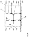
- FIG. 6 an alternative embodiment of a two-channel level detection circuit 46 is shown, which also has a complete galvanic isolation to the control device 50.
- the two-channel testable level detection circuit 46 provides a preferably high-impedance sense current path which is arranged in parallel with the switchable main current path of the circuit device.
- This measuring current path comprises a first and a second measuring channel, each channel having a respective Zener diode 4612 or 4622 and a voltage divider comprising a first resistor 4610 or 4620 and a second resistor 4611 or 4621.
- a light-emitting diode 4631 or 4641 of a first optocoupler 463 or 464 is connected in parallel in each case.
- the light-emitting diode has in each case a forward voltage of, for example, 1.1 V.
- the Z-diodes 4612 and 4622 of both measuring channels each have a Z voltage of, for example, 14 V.
- the two measuring channels can each be bridged via a switchable transistor of a second optocoupler 465 or 466 for testing the level detection circuit 46.
- a measuring path can also have more than the two measuring channels shown, wherein the dimensioning of the Z-diodes must be adjusted according to the number of channels.
- the measurement path of the level detection circuit 46 When the supply voltage applied to the two voltage terminals 1 and 3 is in the range of the rated voltage of 24 VDC, no current flows through the measurement path of the level detection circuit 46. If the supply voltage exceeds the sum of the Z voltages of both Zener diodes 4612 and 4622, i. for example, a value of 28 V, the measurement path becomes conductive.
- the measuring path is particularly in view of large overvoltages e.g. of up to 120 V high impedance designed to limit the flow of current and the thermal load and to ensure a corresponding dielectric strength.
- a resistor 467 may also be provided at the output of the measuring current path.
- the illustrated resistor network is dimensioned such that at the latest when reaching the maximum allowable supply voltage of 32 V, the optocouplers 463 and 464, i. their integrated LEDs 4631 and 4641 are turned on. Via the signal line pairs 563, 564 and 567 and 568, an overvoltage situation can be signaled to the control device 50 in two channels.
- the two exemplary measurement channels each include a second optocoupler 465 and 466, which enable testability of the level detection circuit 46.
- a Triggered test signal from the controller 50, one of the two optocouplers is activated in each case, so that the corresponding measuring channel is bridged.
- a supply voltage in the range of the nominal voltage of 24 V exceeds the Z voltage of the Zener diode of the remaining, ie not bridged, measuring channel, so that it switches through.
- the forward voltage of the respective light emitting diode in the optocoupler of the remaining measuring channel is also exceeded, so that the optocoupler is activated.
- the control device 50 receives, assuming a functioning level detection circuit 46, in each case a feedback signal via the respective non-bridged measuring channel.
- the measurement channels are cyclically alternately tested. If a feedback signal to a transmitted test signal, the controller 50 may indicate a malfunction within the level detection circuit 46.
Landscapes
- Emergency Protection Circuit Devices (AREA)
- Protection Of Static Devices (AREA)
- Dc-Dc Converters (AREA)
Description
Die vorliegende Erfindung betrifft eine Schaltungsvorrichtung für einen Überspannungsschutz elektronischer Baugruppen.The present invention relates to a circuit device for overvoltage protection of electronic assemblies.
Für die Approbation von 24 VDC Baugruppen, die in der Automatisierungstechnik und insbesondere in der Sicherheitstechnik Verwendung finden, sind gemäß DIN EN 60950-1 Kapitel 2.2.2 zunehmend strengere Anforderungen an die Festigkeit gegen Überspannungen zu erfüllen.For the approval of 24 VDC modules, which are used in automation technology and in particular in safety technology, increasingly stringent requirements for the resistance to overvoltages must be met in accordance with DIN EN 60950-1 Chapter 2.2.2.
Ein entsprechend geeigneter Schutz vor Überspannungen, die über die 24 VDC Versorgungsanschlüsse in eine elektronische Baugruppe einkoppeln können, kann zum Beispiel durch ein Relais im Versorgungsstrompfad bereitgestellt werden, mit dem eine nachgeschaltete, zu schützende elektronische Baugruppe von den Versorgungsanschlüssen getrennt werden kann, sobald an den Versorgungsanschlüssen eine Überspannung auftritt.Correspondingly suitable protection against overvoltages that can couple into an electronic module via the 24 VDC supply connections can, for example, be provided by a relay in the supply current path, with which a downstream electronic module to be protected can be disconnected from the supply connections as soon as possible Supply connections an overvoltage occurs.
Innerhalb eines zulässigen Versorgungsspannungsbereichs zieht das Relais an, so dass eine nachfolgende Baugruppe mit Spannung versorgt wird. Der Ruhestrom zum Durchschalten des Relais wird über eine Schaltung aus dem Versorgungsstrompfad gewonnen.Within a permissible supply voltage range, the relay picks up, so that a subsequent module is supplied with voltage. The quiescent current for switching on the relay is obtained via a circuit from the supply current path.
Eine solche Schaltung kann z.B. eine selbstrückstellende Sicherung und eine Überspannungsschutzdiode umfassen, die im Zusammenwirken einen Überspannungsdetektor bilden. Die Überspannungsschutzdiode ist parallel zur Relaisspule angeordnet, wobei die Ansprechspannung dieser Diode auf die maximal zulässige Versorgungsspannung ausgelegt ist. Die Sicherung bildet zusammen mit der Diode und der Relaisspule eine Reihenschaltung. Im Falle einer Überspannung wird durch den hohen Strom, der durch die durchgeschaltete Überspannungsschutzdiode fließt, die selbstrückstellende Sicherung ausgelöst. Das Relais wird von der Versorgung getrennt und fällt dem Ruhestromprinzip zufolge in seine Ruhelage zurück und unterbricht den Stromfluss in Richtung der nachgeschalteten elektronischen Baugruppe.Such a circuit may include, for example, a self-resetting fuse and an overvoltage protection diode that cooperatively form an overvoltage detector. The overvoltage protection diode is parallel to the relay coil arranged, wherein the response voltage of this diode is designed for the maximum allowable supply voltage. The fuse forms a series circuit together with the diode and the relay coil. In the event of an overvoltage, the self-resetting fuse is triggered by the high current flowing through the switched-over overvoltage protection diode. The relay is disconnected from the supply and falls back to its rest position according to the quiescent current principle and interrupts the flow of current in the direction of the downstream electronic module.
Nachteilig am Stand der Technik ist, dass zum zuverlässigen Auslösen ein ausreichend hoher Strom durch die Sicherung fließen muss. Ein entsprechend hoher Stromfluss setzt einen niederohmigen Charakter der Überspannung voraus. Hochohmige Überspannungen können hingegen nicht zuverlässig erkannt werden, da ein Widerstand innerhalb des Versorgungskreises den Strom zum Auslösen der Sicherung derart begrenzen kann, dass die Auslöseschwelle der Sicherung nicht überschritten wird.A disadvantage of the prior art is that for reliable triggering a sufficiently high current must flow through the fuse. A correspondingly high current flow requires a low-impedance character of the overvoltage. High-resistance overvoltages, on the other hand, can not be reliably detected, since a resistance within the supply circuit can limit the current for triggering the fuse such that the triggering threshold of the fuse is not exceeded.
Die
Die
Stromversorgungseinrichtung mit Überwachungsschaltung für mindestens zwei auf ein gemeinsames Bezugspotential bezogene Gleichspannungen unterschiedlicher Polarität mit einem Signalübertragungselement.
Die
The
Die
Die gegenüber vorliegender Erfindung nachveröffentlichte
Der Erfindung liegt die Aufgabe zugrunde, eine Vorrichtung für einen Überspannungsschutz bereitzustellen, mit der auch hochohmige Überspannungen zuverlässig ermittelt und abschaltet werden können.The invention has for its object to provide a device for overvoltage protection, with the high-voltage overvoltages can be reliably detected and turned off.
Die Lösung der Aufgabe ist durch Gegenstände mit den Merkmalen gemäß den anhängenden unabhängigen Ansprüchen gegeben.The solution of the problem is given by articles having the features according to the appended independent claims.
Zur Lösung dieser Aufgabe schlägt die vorliegende Erfindung eine Schaltungsvorrichtung für einen Überspannungsschutz elektronischer Baugruppen vor, die einen Spannungseingang und einen Spannungsausgang umfasst, die über wenigstens eine Schalteinrichtung schaltbar miteinander verbunden sind.To achieve this object, the present invention proposes a circuit device for overvoltage protection of electronic assemblies comprising a voltage input and a voltage output, which are connected via at least one switching device switchable.
Die Schaltungsvorrichtung umfasst ferner eine Messschaltung zum Erfassen einer Spannung am Spannungseingang und eine Steuerungseinrichtung. Die Steuerungseinrichtung ist ausgebildet, die Schalteinrichtung in Abhängigkeit der mit der Messschaltung erfassten Spannung derart anzusteuern, dass bei einer Überspannung am Spannungseingang der Spannungsausgang mittels der Schalteinrichtung vom Spannungseingang getrennt ist.The circuit device further comprises a measuring circuit for detecting a voltage at the voltage input and a control device. The control device is designed to control the switching device as a function of the voltage detected by the measuring circuit such that, in the event of an overvoltage at the voltage input, the voltage output is disconnected from the voltage input by means of the switching device.
Die Steuerungseinrichtung ist über einen Spannungswandler derart mit dem Spannungseingang verbunden, dass auch bei einer Überspannung eine Spannungsversorgung für die Steuerungseinrichtung gewährleistet ist.The control device is connected to the voltage input via a voltage converter such that a voltage supply for the control device is ensured even with an overvoltage.
Ein wesentlicher Vorteil einer Schaltungsvorrichtung gemäß vorliegender Erfindung ist, dass die Steuerungseinrichtung hinter einem Spannungswandler geschützt angeordnet ist, der einen weiten Eingangsspannungsbereich besitzt. Der maximal zulässige Eingangsspannungsbereich des Wandlers beträgt ein Mehrfaches einer maximal zulässigen Versorgungsspannung einer zu schützenden elektronischen Baugruppe.An essential advantage of a circuit device according to the present invention is that the control device is arranged behind a voltage converter which has a wide input voltage range. The maximum permissible input voltage range of the converter is a multiple of a maximum permissible supply voltage of an electronic module to be protected.
Im Überspannungsfall, d.h. wenn der zulässige Bereich für die Versorgungsspannung überschritten ist, wird somit weiterhin eine Funktionsfähigkeit der Schaltungsvorrichtung für einen Überspannungsschutz elektronischer Baugruppen gewährleistet.In the case of overvoltage, i. If the permissible range for the supply voltage is exceeded, a functionality of the circuit device for overvoltage protection of electronic assemblies is thus further ensured.
Die Spannungsfestigkeit der Schaltungsvorrichtung, d.h. der Spannungsbereich, indem ein Überspannungsschutz zuverlässig bereit steht, ist nur durch den Eingangsspannungsbereich des Spannungswandlers nach oben begrenzt.The dielectric strength of the circuit device, ie the voltage range, by a surge protector reliable is ready is limited only by the input voltage range of the voltage converter up.
Die Messschaltung einer erfindungsgemäßen Schaltvorrichtung kann einen Messstrompfad mit wenigstens einem Messkanal besitzen, wobei jedem Messkanal bevorzugt jeweils ein Pegelschalter zugeordnet sein kann.The measuring circuit of a switching device according to the invention may have a measuring current path with at least one measuring channel, wherein each measuring channel may preferably each have a level switch assigned to it.
Die Pegelschalter sind bevorzugt dazu ausgebildet, das Überschreiten eines vorbestimmten Spannungspegels zu erkennen und über eine zugeordnete Signalleitung an die Steuerungseinrichtung zu signalisieren.The level switches are preferably designed to detect the exceeding of a predetermined voltage level and to signal via an associated signal line to the control device.
Jedem Messkanal kann ein Schaltelement zugeordnet sein, das von der Steuerungseinrichtung ansteuerbar ist und das zum Testen der Messschaltung ausgebildet ist.Each measuring channel may be assigned a switching element which can be controlled by the control device and which is designed to test the measuring circuit.
Der Pegelschalter kann beispielsweise einen Komparator umfassen, der mit einer Referenzspannungsquelle verbunden ist. Alternativ kann der Pegelschalter einen Transistor umfassen.The level switch may include, for example, a comparator connected to a reference voltage source. Alternatively, the level switch may comprise a transistor.
In einer besonders vorteilhaften Ausführung der Erfindung kann der Pegelschalter einen ersten Optokoppler und das Schaltelement einen zweiten Optokoppler umfassen.In a particularly advantageous embodiment of the invention, the level switch may comprise a first optocoupler and the switching element may comprise a second optocoupler.
Die Optokoppler ermöglichen eine galvanische Trennung zwischen der Messschaltung und der mit dieser in Verbindung stehenden Steuerungseinrichtung. Des Weitern wird der Pegelschalter im Wesentlichen durch eine Leuchtdiode des ersten Optokopplers gebildet, so dass ein zusätzlicher Komparator nicht erforderlich ist.The optocouplers allow a galvanic isolation between the measuring circuit and the controller connected thereto. Furthermore, the level switch is essentially formed by a light-emitting diode of the first optocoupler, so that an additional comparator is not required.
Der Messstrompfad kann einen Messkanal besitzen, der eine Reihenschaltung aus einer Z-Diode, einem ersten Widerstand und einem zweiten Widerstand umfasst. Der erste Optokoppler ist bevorzugt zum zweiten Widerstand parallel geschaltet.The measuring current path may have a measuring channel which comprises a series connection of a Zener diode, a first resistor and a second resistor. The first optocoupler is preferably connected in parallel with the second resistor.
Die Z-Diode ist im Messkanal vorzugsweise in Sperrrichtung geschaltet, so dass für einen Stromfluss durch den Messpfad ein vorbestimmter Spannungswert überschritten werden muss. Der erste und zweite Widerstand bilden einen Spannungsteiler, der derart dimensioniert ist, dass beim Erreichen einer Überspannung an der Leuchtdiode eine zum Durchschalten ausreichende Vorwärtsspannung anliegt.The Zener diode is preferably switched in the reverse direction in the measurement channel, so that a predetermined voltage value must be exceeded for a current flow through the measurement path. The first and second resistors form a voltage divider which is dimensioned such that upon reaching an overvoltage at the light emitting diode, a forward voltage sufficient for switching through is applied.
Der zweite Optokoppler ist zur Z-Diode bevorzugt parallel geschaltet, so dass diese, durch die Steuerungsvorrichtung, z.B. mittels eines Testsignals angesteuert, zum Testen der Messschaltung überbrückbar ist.The second optocoupler is preferably connected in parallel with the Zener diode, so that the latter, by the control device, e.g. triggered by a test signal, for testing the measuring circuit can be bridged.
Mit dem Überbrücken der Z-Diode wird die durch die Dimensionierung des Messkanals vorgegebene Schaltschwelle abgesenkt, so dass der Pegelschalter bzw. der erste Optokoppler auch bei einer zulässigen Versorgungsspannung an den Spannungseingängen auslösen kann. Im Falle einer funktionsfähigen Messschaltung empfängt die Steuerungseinrichtung auf das ausgesendete Testsignal ein resultierendes Feedback-Signal.By bridging the Zener diode, the switching threshold predetermined by the dimensioning of the measuring channel is lowered so that the level switch or the first optocoupler can trip at the voltage inputs even if the supply voltage is permissible. In the case of a functional measuring circuit, the control device receives a resulting feedback signal on the transmitted test signal.
In einer alternativen Ausgestaltung kann der Messstrompfad eine Anzahl aus wenigstens zwei in Reihe geschalteter Messkanäle umfassen. Jeder Messkanal umfasst bevorzugt eine Reihenschaltung aus einer Z-Diode, einen ersten Widerstand und einen zweiten Widerstand. Der erste Optokoppler eines jeweiligen Messkanals ist jeweils bevorzugt zum zweiten Widerstand des Messkanals parallel geschaltet.In an alternative embodiment, the measuring current path may comprise a number of at least two measuring channels connected in series. Each measuring channel preferably comprises a series connection of a Zener diode, a first resistor and a second resistor. The first optocoupler of each measuring channel is preferably connected in parallel to the second resistor of the measuring channel.
Der zweite Optokoppler kann zum zugeordneten Messkanal parallel geschaltet sein, so dass der jeweilige Messkanal zum Testen der Messschaltung überbrückbar ist.The second optocoupler can be connected in parallel to the assigned measuring channel, so that the respective measuring channel can be bridged for testing the measuring circuit.
Die Messschaltung kann in einer alternativen Ausführung der Erfindung einen Spannungsteiler und einen Digital/Analog-Wandler zum Messen und Digitalisieren einer Spannung am Spannungseingang umfassen. Die Steuerungseinrichtung kann eine Einrichtung zum Vergleichen des digitalisierten Spannungswerts mit einem zulässigen Grenzwert umfassen.In an alternative embodiment of the invention, the measuring circuit may comprise a voltage divider and a digital / analog converter for measuring and digitizing a voltage at the voltage input. The controller may include means for comparing the digitized voltage value to an allowable limit.
Die Erfindung umfasst auch ein Überspannungsschutzmodul, das eine der zuvor beschriebenen Schaltungsvorrichtungen umfasst, dass zum Anschließen einer nachgeschalteten elektronische Baugruppe geeignet ist. Ein solches Modul ist insbesondere zur Nachrüstung eines Überspannungsschutzes für bestehende Baugruppen geeignet. Der Spannungsausgang der Schaltungsvorrichtung ist bevorzugt mit einem Eingang einer zu schützenden elektronischen Baugruppe verbindbar. Der Spannungseingang ist an eine Versorgungsspannungsquelle anschließbar.The invention also includes an overvoltage protection module comprising one of the previously described circuit devices suitable for connection to a downstream electronic subassembly. Such a module is particularly suitable for retrofitting an overvoltage protection for existing modules. The voltage output of the circuit device is preferably connectable to an input of an electronic module to be protected. The voltage input can be connected to a supply voltage source.
Die erfindungsgemäße Schaltungsvorrichtung kann auch als ein Bestandteil einer elektronischen Baugruppe verwendet werden, wobei diese bevorzugt unmittelbar am Eingang einer solchen Baugruppe anzuordnen ist.The circuit device according to the invention can also be used as a component of an electronic module, which is preferably to be arranged directly at the entrance of such an assembly.
Die Erfindung wird nachfolgend anhand beispielhafter Ausführungsformen unter Bezugnahme der beigefügten Zeichnungen detaillierter beschrieben. In den Zeichnungen zeigen:
- Fig. 1:
- ein Bockschaltbild einer Schaltungsvorrichtung für einen Überspannungsschutz elektronischer Baugruppen;
- Fig. 2:
- eine testbare Messschaltung zur Detektion von Überspannungen am Spannungseingang einer Schaltungsvorrichtung gemäß
Fig. 1 ; - Fig. 3:
- eine testbare Messschaltung zur Messen einer am Spannungseingang anliegenden Spannung;
- Fig. 4:
- eine alternative Messschaltung zur Detektion von Überspannungen am Spannungseingang der Schaltungsvorrichtung gemäß
Fig. 1 ; - Fig. 5:
- einer erste bevorzugte Ausführung einer Messschaltung zur Detektion von Überspannungen am Spannungseingang, mit einem testbaren Pegelschalter und einer galvanische Trennung zur Steuerungseinrichtung;
- Fig. 6:
- einer weitere bevorzugte Ausführungsform einer Messschaltung zur Detektion von Überspannungen.
- Fig. 1:
- a block diagram of a circuit device for overvoltage protection of electronic assemblies;
- Fig. 2:
- a testable measuring circuit for detecting overvoltages at the voltage input of a circuit device according to
Fig. 1 ; - 3:
- a testable measuring circuit for measuring a voltage applied to the voltage input;
- 4:
- an alternative measuring circuit for detecting overvoltages at the voltage input of the circuit device according to
Fig. 1 ; - Fig. 5:
- a first preferred embodiment of a measuring circuit for detecting overvoltages at the voltage input, with a testable level switch and a galvanic isolation to the control device;
- Fig. 6:
- a further preferred embodiment of a measuring circuit for detecting overvoltages.
Die
Die elektronischen Baugruppen in der Automatisierungs- bzw. Sicherheitstechnik sind in der Regel auf eine Nennspannung von 24 VDC ausgelegt, wobei ein Versorgungsspannungsbereich zwischen 18 VDC und 32 VDC (inklusive Welligkeiten und aller Toleranzen) in der Regel zulässig ist.The electronic modules in the automation and safety technology are usually designed for a rated voltage of 24 VDC, with one supply voltage range between 18 VDC and 32 VDC (including ripples and all tolerances) is usually allowed.
Wird der obere Grenzwert (z.B. 32 VDC) eines zulässigen Versorgungsspannungsbereichs überschritten, so liegt eine Überspannung vor, die ggf. auch zu einer Zerstörung einer nachgeschalteten elektronischen Baugruppe führen kann.If the upper limit value (for example 32 VDC) of a permissible supply voltage range is exceeded, then there is an overvoltage which, if necessary, can also lead to the destruction of a downstream electronic module.
Die in der
Der Spannungsanschluss 4 ist beispielhaft mit dem eingangsseitigen Bezugspotentialanschluss 3 fest verbunden, während der Ausgangsspannungsanschluss 2 im dargestellten Beispiel zweckmäßig über zwei in Reihe geschaltete Schalteinrichtungen 30 und 31 von der Spannung am Eingangsspannungsanschluss 1 trennbar ist.The
Die erfindungsgemäße Schaltungsvorrichtung kann sowohl ein Bestandteil einer elektronischen Baugruppe sein, als auch in einem separaten Überspannungsmodul eingesetzt werden, an das eine elektronische Baugruppe angeschlossen werden kann.The circuit device according to the invention can both be a component of an electronic module, as well as be used in a separate overvoltage module, to which an electronic module can be connected.
Mit den zweckmäßig zwei in Reihe geschalteten Schalteinrichtungen 30 und 31 kann auch die Anforderung der Sicherheitstechnik an eine mehrkanalige Ausführung sicherheitsrelevanter Funktionen, d.h. einer sicheren Trennung der beiden Spannungsanschlüsse 1 und 2 gewährleistet werden. Die Schaltungsvorrichtung kann selbstverständlich auch mit einem einkanalig abschaltbaren Versorgungspfad zwischen den Spannungsanschlüssen 1 und 2 realisiert werden. Optional können die Schalteinrichtungen 30, 31 auch zweipolig ausgeführt sein, so dass sowohl der Spannungsanschluss 1, als auch der Bezugspotentialanschluss 3 schaltbar mit den zugeordneten Spannungsanschlüssen 2 und 4 am Ausgang verbunden ist.With the appropriately two series-connected
Die Schalteinrichtungen 30 und 31 sind in der
Die Schalteinrichtungen 30 und 31 werden jeweils über einen separaten Steuerkanal von einer Steuereinrichtung 50 redundant angesteuert. Die Steuereinrichtung 50 ist mit einer Messschaltung 40 verbunden, mit der eine zwischen den eingangsseitigen Spannungsanschlüssen 1 und 3 anliegende Versorgungsspannung erfasst, gemessen und/oder überwacht werden kann.The
Die Spannungsversorgung für die Steuereinrichtung 50 wird mittelbar über die eingangsseitigen Spannungsanschlüsse 1 und 3 bereitgestellt, wobei die Steuereinrichtung 50 hinter einem Spannungswandler 60 angeordnet ist. Eingangseitig ist der Spannungswandler 60 für Gleich- und Wechselspannungen in einem weiten Spannungsbereich zum Beispiel bis zu 120 V ausgelegt, so dass ausgangsseitig eine geregelte, d.h. von dem weiten Eingangspannungsbereich unabhängige Betriebsspannung für die Steuereinrichtung 50 bereitsteht.The power supply for the
Die Steuereinrichtung 50 zur Überwachung der an der Schaltungsvorrichtung anliegenden Versorgungsspannung ist also gegen Überspannungen, d.h. gegen Spannungen, die über die zulässigen Spannungen, z.B. 32 VDC, hinausgehen, geschützt hinter dem Spannungswandler 60 angeordnet. Mit einer maximalen Eingangsspannung von z.B. 120 V ist der Spannungswandler wesentlich spannungsfester, als die an den Anschlüssen 2 und 4 anschließbaren elektronischen Baugruppen, die durch die Schaltungsvorrichtung geschützt werden sollen.The
Die Steuereinrichtung 50 steuert über eine interne Logik, die zum Beispiel durch einen Mikrocontroller bereitgestellt werden kann, die Schalteinrichtungen 30 und 31 derart an, dass der Ausgangsspannungsanschluss 2 beim Erkennen einer Überspannung vom Spannungsanschluss 1 getrennt wird, bevor eine nachgeschaltete und vor Überspannungen zu schützende elektronische 24 V-Baugruppe gefährdet bzw. zerstört wird. Die Schalteigenschaften der Schalteinrichtungen 30 und 31 sind, wie der Spannungswandler 60 auch, auf eine maximal zu erwartende Überspannung, z.B. 120 V, und einen entsprechenden maximalen Strom ausgelegt.The
Die Steuereinrichtung 50 ist über eine Anzahl von Leitungen 5 zum Steuern, Messen bzw. Signalisieren mit der Messschaltung 40 verbunden, so dass im Zusammenwirken dieser beiden Komponenten die Spannung zwischen dem Spannungsanschluss 1 und dem Bezugspotentialanschluss 3 bewertet werden kann. Die Messschaltung 40 ist insbesondere auch zum Erkennen von hochohmigen Überspannungen geeignet. Die Leitungen 5 sind in den
Erfindungsgemäß kann, wie aus den weiteren Figuren deutlich werden wird, die Messschaltung 40 von den Steuereinrichtung 50 über die Leitungen 5 zyklisch auf ihre Funktionsfähigkeit hin getestet werden. Somit ist ein zuverlässiges Trennen der nachgeschalteten elektronischen Baugruppen von einer Überspannung jederzeit gewährleistet. Wird eine Fehlfunktion in der Messschaltung 40 erkannt, so wird der Ausgangsspannungsanschluss 2 über die Schalteinrichtungen 30 bzw. 31 von dem Eingangsspannungsanschluss getrennt. Ein von der Steuereinrichtung 50 erkannter Fehler kann somit zumindest im Wege der Abschaltung einer nachgeschalteten elektronischen Baugruppe signalisiert werden.According to the invention, as will become apparent from the other figures, the measuring
Die Logik der Steuereinrichtung 50 kann je nach Ausführung der Schaltungsvorrichtung ein oder mehrkanalig ausgeführt werden, um eine entsprechende Anzahl von Schalteinrichtungen redundant anzusteuern. Optional können auch mehrere parallele Messschaltungen 40 zur Überwachung der Versorgungsspannung vorgesehen werden, um die Redundanz und Sicherheit der Schaltungsvorrichtung weiter zu erhöhen.Depending on the design of the circuit device, the logic of the
Optional können an der Steuereinrichtung 50 sichere Logikeingänge 51 und Logikausgänge 52 vorgesehen sein, mit denen Sicherheitsfunktionen wie NOT-AUS-Applikationen zu ermöglichen sind.Optionally,
Die Messschaltung 40 zur Überwachung der Eingangsspannung kann, wie in den folgenden Figuren deutlich werden wird, je nach Anforderung mit oder ohne eine galvanische Trennung zwischen Steuereinrichtung 50 und den Spannungsanschlüsse 1 und 3 ausgeführt werden. Die Messschaltung 40 kann einen testbare Pegelerkennungsschaltung 42, 44, 45 oder 46 oder eine Spannungsmesseinrichtung 43 beinhalten.The measuring
In
Der Spannungsteiler ist derart dimensioniert, dass beim Auftreten einer Überspannung zwischen den Spannungsanschlüssen 1 und 3 eine Spannung an dem nicht invertierenden Eingang des Komparators abfällt, die größer ist, als die Referenzspannung URef, die von der Referenzspannungsquelle 422 bereitgestellt wird. In diesem Fall wird über eine Signalleitung 522 am Ausgang des Komparators 423 ein Signal an die Steuereinrichtung 50 gesendet.The voltage divider is dimensioned such that when an overvoltage occurs between the
Der Spannungsteiler ist bevorzugt hochohmig ausgelegt, um eine Überlastung der Spannungsversorgungseinrichtung an den Spannungsanschlüsse 1 und 3 insbesondere im Falle einer Überspannung zu vermeiden.The voltage divider is preferably designed with high resistance in order to avoid overloading of the voltage supply device at the
Die Pegelerkennungsschaltung 42 umfasst ferner einen durch die Steuereinrichtung 50 ansteuerbaren Transistor 424, der zum Testen der Überspannungserkennung dient. Der Transistor 424 ist zum ersten Widerstand 420 parallel geschaltet, mit dem der Spannungsteiler derart verstimmbar ist, dass die Spannung am nicht invertierenden Eingang des Komparators 423 innerhalb einer zulässigen Versorgungsspannung die Referenzspannung überschreitet. Der Transistor 424 kann dazu innerhalb eines Testzyklus von der Steuereinrichtung 50 über die Steuerleitung 521 angesteuert werden. Sofern die Pegelerkennungsschaltung 42 ordnungsgemäß arbeitet, wird über die Messleitung 522 ein entsprechendes Antwort- bzw. Feedback-Signal aus dem Komparator 423 von der Steuereinrichtung 50 empfangen. Um den Spannungsabfall an dem nichtinvertierenden Eingang des Komparators bei einem durchgestalteten Transistor 424 zu begrenzen, kann ein weiterer Widerstand zu dem Transistor 424 in Reihe geschaltet werden.The
Die
Eine alternative Pegelerkennungsschaltung 44 zur Erkennung einer Überspannung ist in der
Der Spannungsteiler ist z.B. derart dimensioniert, dass bei dem überschreiten einer maximal zulässigen Versorgungsspannung von 32 V die Durchlassspannung am Basis-Emitter-Übergang überschritten wird. Der Transistor schaltet durch, so dass ein entsprechender Pegelwechsel auf der Leitung 543 eine Überspannung an die Steuereinrichtung 50 signalisiert.The voltage divider is dimensioned, for example, such that when exceeding a maximum permissible supply voltage of 32 V, the forward voltage at the base-emitter junction is exceeded. The transistor switches through, so that a corresponding level change on the
Über den Transistor 445 kann die Messschaltung 44 durch die gesteuerte Veränderung des Teilerverhältnisses zyklisch getestet werden.Via the
In den
Die testbare Pegelerkennungsschaltung 45, die in der
Sofern sich die zwischen den Spannungsanschlüssen 1 und 3 anliegende Versorgungsspannung im Bereich der Nennspannung von 24 VDC befindet, d.h. mit einer Abweichung bis +6 V, sperrt die Z-Diode, so dass kein Strom durch den Messpfad fließt. Somit tritt kein messbares Ereignis auf.Provided that the voltage applied between the
Überschreitet die zwischen den Spannungsanschlüssen 1 und 3 anliegende Versorgungsspannung die Z-Spannung von 30 V, so leitet der Messpfad, wobei der resultierende Stromfluss durch die zwei in Reihe geschalteten Widerstände 450 und 451 begrenzt wird. Über die beiden Widerstände 450 und 451 fällt die anliegende Versorgungsspannung abzüglich den 30 V ab, die an der Z-Diode 452 abfallen. Die Widerstände 450 und 451 bilden einen Spannungsteiler, der zweckmäßig so dimensioniert ist, dass bei einer Versorgungsspannung über 32 V an dem zweiten Widerstand 451 ein Spannung abfällt, die der Durchlassspannung der Leuchtdiode 4531 des Optokopplers 453 entspricht. Mit dem Übergang in den Durchlassbereich erkennt und signalisiert die Leuchtdiode 4531 das Vorliegen einer Überspannung.Exceeds the voltage applied between the
Mit dem Überschreiten der maximalen Versorgungsspannung von 32 V wird also die Schaltschwelle des Optokopplers 453 erreicht, so dass die Überspannung über den Fototransistor 4532 und die Signalleitungen 553 und 554 an die Steuereinrichtung 50 übermittelt wird. Mit dem Fototransistor 4542 des zweiten Optokopplers 454 kann die Z-Diode 452 zum Testen des Pegelschalters 45 überbrückt werden. Die Leuchtdiode 4541 im Eingang des zweiten Optokopplers 454 wird von der Steuerungseinrichtung 50 über die Steuerleitungen 551 und 552 angesteuert. In einem Testzyklus wird der Messpfad mit dem Überbrücken der Z-Diode auch im Nennspannungsbereich leitend, so dass ein resultierender Spannungsabfall an dem ersten Widerstand 450 den Wert der Durchlassspannung der Leichtdiode 4531 des ersten Optokopplers überschreitet. Die Steuerungseinrichtung 50 empfängt daraufhin ein erwartetes Signal aus dem ersten Optokoppler, sofern die dargestellte Pegelerkennungsschaltung 45 funktionsfähig ist.When the maximum supply voltage of 32 V is exceeded, the switching threshold of the
Die in der
In der
Die zweikanalige testbare Pegelerkennungsschaltung 46 stellt einen vorzugsweise hochohmigen Messstrompfad bereit, der parallel zu dem schaltbaren Hauptstrompfad der Schaltungsvorrichtung angeordnet ist. Dieser Messstrompfad umfasst einen ersten und einen zweiten Messkanal, wobei jeder Kanal jeweils eine Z-Diode 4612 bzw. 4622 und einen Spannungsteiler aus einem ersten Widerstand 4610 bzw. 4620 und einem zweiten Widerstand 4611 bzw. 4621 besitzt. Zum zweiten Widerstand des jeweiligen Messkanals ist jeweils eine Leuchtdiode 4631 bzw. 4641 eines ersten Optokopplers 463 bzw. 464 parallel geschaltet. Die Leuchtdiode besitzt jeweils eine Durchlassspannung von z.B. 1,1 V. Die Z-Dioden 4612 und 4622 beider Messkanäle besitzen jeweils eine Z-Spannung von beispielsweise 14 V.The two-channel testable
Die beiden Messkanäle sind jeweils über einen schaltbaren Transistor eines zweiten Optokopplers 465 bzw. 466 zum Testen der Pegelerkennungsschaltung 46 überbrückbar.The two measuring channels can each be bridged via a switchable transistor of a
Ein Messpfad kann auch mehr als die zwei dargestellten Messkanäle besitzen, wobei die Dimensionierung der Z-Dioden entsprechend an die Anzahl der Kanäle angepasst sein muss.A measuring path can also have more than the two measuring channels shown, wherein the dimensioning of the Z-diodes must be adjusted according to the number of channels.
Wenn sich die an den beiden Spannungsanschlüssen 1 und 3 anliegende Versorgungsspannung im Bereich der Nennspannung von 24 VDC befindet, fließt kein Strom durch den Messpfad der Pegelerkennungsschaltung 46. Überschreitet die Versorgungsspannung die Summe der Z-Spannungen beider Z-Dioden 4612 und 4622, d.h. beispielsweise einen Wert von 28 V, so wird der Messpfad leitend. Der Messpfad ist insbesondere im Hinblick auf große Überspannungen z.B. von bis zu 120 V hochohmig ausgelegt, um den Stromfluss und die thermische Belastung zu begrenzen und eine entsprechende Spannungsfestigkeit zu gewährleisten. Zur Strombegrenzung kann auch ein Widerstand 467 am Ausgang des Messstrompfads vorgesehen sein. Das dargestellte Widerstandsnetzwerk ist so dimensioniert, dass spätestens beim Erreichen der maximal zulässigen Versorgungsspannung von 32 V die Optokoppler 463 und 464, d.h. ihre integrierten Leuchtdioden 4631 und 4641 durchgeschaltet sind. Über die Signalleitungspaare 563, 564 sowie 567 und 568 ist eine Überspannungssituation an die Steuereinrichtung 50 zweikanalig signalisierbar.When the supply voltage applied to the two
Die beiden beispielhaften Messkanäle umfassen jeweils einen zweiten Optokoppler 465 und 466, die eine Testbarkeit der Pegelerkennungsschaltung 46 ermöglichen. Durch ein Testsignal von der Steuereinrichtung 50 angesteuert, wird jeweils einer der beiden Optokoppler aktiviert, so dass der korrespondierende Messkanal überbrückt ist. Eine Versorgungsspannung im Bereich der Nennspannung von 24 V überschreitet die Z-Spannung der Z-Diode des verbleibenden, d.h. nicht überbrückten Messkanals, so dass diese Durchschaltet. Die Durchlassspannung der jeweiligen Leuchtdiode im Optokoppler des verbleibenden Messkanals wird ebenfalls überschritten, so dass der Optokoppler aktiviert wird. Die Steuereinrichtung 50 empfängt, unter Voraussetzung einer funktionsfähigen Pegelerkennungsschaltung 46, jeweils ein Feedback-Signal über den jeweils nicht überbrückten Messkanal. Vorzugsweise werden die Messkanäle zyklisch alternierend getestet. Bleib ein Feedback Signal auf ein gesendetes Testsignal aus, so kann die Steuereinrichtung 50 auf ein Fehlfunktion innerhalb der Pegelerkennungsschaltung 46 schließen.The two exemplary measurement channels each include a
- 11
- EingangsspannungsanschlussInput Voltage Termination
- 22
- AusgangsspannungsanschlussOutput voltage terminal
- 33
- BezugspotentialanschlussReference potential terminal
- 3030
- Schalteinrichtungswitching device
- 3131
- Schalteinrichtungswitching device
- 44
- BezugspotentialanschlussReference potential terminal
- 4040
- Messschaltungmeasuring circuit
- 4242
- PegelerkennungsschaltungLevel detection circuit
- 420420
- ersten Widerstandfirst resistance
- 421421
- zweiter Widerstandsecond resistance
- 422422
- ReferenzspannungsquelleReference voltage source
- 423423
- Komparatorcomparator
- 424424
- Transistor/SchaltelementTransistor / switching element
- 4343
- SpannungsmesseinrichtungVoltage measuring device
- 430430
- erster Widerstandfirst resistance
- 431431
- zweiter Widerstandsecond resistance
- 432432
- Analog/Digital-WandlerAnalog / digital converter
- 433433
- Transistor/SchaltelementTransistor / switching element
- 4444
- PegelerkennungsschaltungLevel detection circuit
- 440440
- erster Widerstandfirst resistance
- 441441
- zweiter Widerstandsecond resistance
- 442442
- Kollektorwiderstandcollector resistance
- 443443
- Transistor/PegelschalterTransistor / level switch
- 444444
- Emitterwiderstandemitter resistor
- 435435
- Transistor/SchaltelementTransistor / switching element
- 4545
- PegelerkennungsschaltungLevel detection circuit
- 450450
- erster Widerstandfirst resistance
- 451451
- zweiter Widerstandsecond resistance
- 452452
- Z-DiodeZener diode
- 453453
- erster Optokopplerfirst optocoupler
- 45314531
- Leuchtdiode/PegelschalterLED / level switch
- 45324532
- Fototransistorphototransistor
- 454454
- zweiter Optokopplersecond optocoupler
- 45414541
- Leuchtdiodeled
- 45424542
- Fototransistor/SchaltelementPhototransistor / switching element
- 4646
- PegelerkennungsschaltungLevel detection circuit
- 46104610
- erster Widerstand (1. Kanal)first resistance (1st channel)
- 46114611
- zweiter Widerstand (1. Kanal)second resistor (1st channel)
- 46124612
- Z-Diode (1. Kanal)Z-diode (1st channel)
- 46204620
- erster Widerstand (2. Kanal)first resistance (2nd channel)
- 46214621
- zweiter Widerstand (2. Kanal)second resistor (2nd channel)
- 46224622
- z-Diode (2. Kanal)z-diode (2nd channel)
- 463463
- erster Optokoppler (1. Kanal)first optocoupler (1st channel)
- 46314631
- Leuchtdiode/PegelschalterLED / level switch
- 46324632
- Fototransistorphototransistor
- 465465
- zweiter Optokoppler (1. Kanal)second optocoupler (1st channel)
- 46514651
- Leuchtdiodeled
- 46524652
- Fototransistor/SchaltelementPhototransistor / switching element
- 464464
- erster Optokoppler (2. Kanal)first optocoupler (2nd channel)
- 46414641
- Leuchtdiode/PegelschalterLED / level switch
- 46424642
- Fototransistorphototransistor
- 466466
- zweiter Optokoppler (2. Kanal)second optocoupler (2nd channel)
- 46614661
- Leuchtdiodeled
- 46624662
- Fototransistor/SchaltelementPhototransistor / switching element
- 467467
- Widerstandresistance
- 55
- Leitungencables
- 5050
- Steuereinrichtungcontrol device
- 5151
- sichere Logikeingängesecure logic inputs
- 5252
- Logikausgängelogic outputs
- 521521
- Steuerleitungcontrol line
- 522522
- Signalleitungsignal line
- 523523
- Leitung (Bezugspotential)Line (reference potential)
- 531531
- Steuerleitungcontrol line
- 532532
- serielle/parallele Verbindungsleitungserial / parallel connection line
- 533533
- Leitung (Bezugspotential)Line (reference potential)
- 541541
- Signalleitungsignal line
- 542542
- Leitung (Versorgungsspannung)Line (supply voltage)
- 543543
- Signalleitungsignal line
- 544544
- Leitung (Bezugspotential)Line (reference potential)
- 551551
- Steuerleitungcontrol line
- 552552
- Steuerleitungcontrol line
- 553553
- Signalleitungsignal line
- 554554
- Signalleitungsignal line
- 561561
- Steuerleitung (1. Kanal)Control line (1st channel)
- 562562
- Steuerleitung (1. Kanal)Control line (1st channel)
- 563563
- Signalleitung (1. Kanal)Signal line (1st channel)
- 564564
- Signalleitung (1. Kanal)Signal line (1st channel)
- 565565
- Steuerleitung (2. Kanal)Control line (2nd channel)
- 566566
- Steuerleitung (2. Kanal)Control line (2nd channel)
- 567567
- Signalleitung (2. Kanal)Signal line (2nd channel)
- 568568
- Signalleitung (2. Kanal)Signal line (2nd channel)
- 6060
- SpannungswandlerDC converter
- 6161
- AusgangsspannungsanschlussOutput voltage terminal
- 6262
- BezugsspannungsanschlussReference voltage terminal
Claims (14)
- Circuit device for overvoltage protection of electronic assemblies, comprising a voltage input (1) and a voltage output (2) which are connected together so as to be switchable via at least one switching device (30), further comprising measuring circuitry (40) for detecting a voltage at the voltage input (1) and a control device (50), wherein the control device (50) is configured to actuate the switching device (30) in dependence upon the voltage detected by the measuring circuitry (40) such that the voltage output (2) is separated from the voltage input (1) by means of the switching device (30) in the event of an overvoltage at the voltage input (1), wherein the control device (50) is connected to the voltage input (1) via a voltage converter (60) such that a voltage supply for the control device (50) is ensured even in the case of overvoltage, characterised in that the measuring circuitry (40) can be tested as to its functionality by a transistor (424; 433; 445; 4542; 4652, 4662) which can be actuated by the control device (50).
- Circuit device as claimed in the preceding claim, characterised in that the measuring circuitry (40) has a measuring current path having at least one measuring channel, wherein a gauge switch (423, 443, 453, 463, 464) is allocated to each measuring channel.
- Circuit device as claimed in the preceding claim, characterised in that the gauge switches are configured to detect when a predetermined voltage level is exceeded and to signal same to the control device (50) via a signal line (5).
- Circuit device as claimed in the preceding claim, characterised in that a switching element (424; 445; 4542; 4652, 4662) is allocated to each measuring channel and can be actuated by the control device (50) and is configured for testing the measuring circuitry (40).
- Circuit device as claimed in claim 4, characterised in that the gauge switch includes a comparator (423) which is connected to a reference voltage source (422).
- Circuit device as claimed in claim 4, characterised in that the gauge switch includes a transistor (443).
- Circuit device as claimed in claim 4, characterised in that the gauge switch includes a first optocoupler (453; 463, 464) and the switching element includes a second optocoupler (454; 465, 466).
- Circuit device as claimed in claim 7, characterised in that the measuring current path has a measuring channel which includes a series connection of a Z diode (452), a first resistor (450) and a second resistor (451), wherein the first optocoupler (453) is connected in parallel with the second resistor (451).
- Circuit device as claimed in claim 7 or 8, characterised in that the second optocoupler (454) is connected in parallel with the Z diode (452) so that the Z diode can be bridged for testing the measuring circuitry (40).
- Circuit device as claimed in claim 7, characterised in that the measuring current path includes at least two series-connected measuring channels, wherein each measuring channel includes a series connection of a Z diode (4612, 4622), a first resistor (4610, 4620) and a second resistor (4611, 4621), wherein the first optocoupler (463, 464) of a measuring channel is connected in parallel with the second resistor.
- Circuit device as claimed in claim 7, characterised in that the second optocoupleur (465, 466) is connected in parallel with the allocated measuring channel so that the respective measuring channel can be bridged for testing the measuring circuitry (40).
- Circuit device as claimed in claim 1, characterised in that the measuring circuitry (40; 43) includes a voltage divider (430, 431) and a digital/analogue converter (432) for measuring and digitising a voltage at the voltage input (1).
- Overvoltage protection module comprising a circuit device as claimed in any one of the preceding claims 1 to 12, characterised in that the voltage output (2) of the circuit device can be connected to an electronic assembly and the voltage input (1) can be connected to a voltage source.
- Use of a circuit device as claimed in any one of claims 1 to 12 within an electronic assembly.
Applications Claiming Priority (2)
| Application Number | Priority Date | Filing Date | Title |
|---|---|---|---|
| DE102011115852 | 2011-10-13 | ||
| DE102012004577.8A DE102012004577B4 (en) | 2011-10-13 | 2012-03-09 | Circuit device for overvoltage protection of electronic assemblies, overvoltage protection module with the circuit device and use of the circuit device |
Publications (2)
| Publication Number | Publication Date |
|---|---|
| EP2582001A1 EP2582001A1 (en) | 2013-04-17 |
| EP2582001B1 true EP2582001B1 (en) | 2016-11-02 |
Family
ID=46798946
Family Applications (1)
| Application Number | Title | Priority Date | Filing Date |
|---|---|---|---|
| EP12005573.6A Active EP2582001B1 (en) | 2011-10-13 | 2012-07-31 | Excess voltage protective device for electronic modules |
Country Status (1)
| Country | Link |
|---|---|
| EP (1) | EP2582001B1 (en) |
Families Citing this family (1)
| Publication number | Priority date | Publication date | Assignee | Title |
|---|---|---|---|---|
| DE102018207503A1 (en) * | 2018-05-15 | 2019-11-21 | Continental Teves Ag & Co. Ohg | Circuit arrangement for protecting an electronic module |
Family Cites Families (6)
| Publication number | Priority date | Publication date | Assignee | Title |
|---|---|---|---|---|
| DE3923710A1 (en) * | 1989-07-18 | 1991-01-24 | Philips Patentverwaltung | POWER SUPPLY WITH DC VOLTAGE MONITORING |
| US20040184208A1 (en) * | 2003-03-19 | 2004-09-23 | Daniel Liu | Power protecting device for electrical power source and load |
| TWM313812U (en) * | 2006-11-27 | 2007-06-11 | Micro Star Int Co Ltd | Computer device with over voltage protection |
| DE102008051514B4 (en) * | 2008-10-14 | 2022-08-25 | Robert Bosch Gmbh | Voltage monitoring arrangement for a security module |
| US8203815B2 (en) * | 2009-05-08 | 2012-06-19 | Hamilton Sundstrand Corporation | System and method to provide transient overvoltage suppression |
| TW201145742A (en) * | 2010-06-03 | 2011-12-16 | Hon Hai Prec Ind Co Ltd | Power supply protecting apparatus |
-
2012
- 2012-07-31 EP EP12005573.6A patent/EP2582001B1/en active Active
Also Published As
| Publication number | Publication date |
|---|---|
| EP2582001A1 (en) | 2013-04-17 |
Similar Documents
| Publication | Publication Date | Title |
|---|---|---|
| EP2817860B1 (en) | Safety switchgear with power supply unit | |
| EP2951901B1 (en) | Safety switching device with a safe power supply unit | |
| EP2418748B1 (en) | Energy supply device | |
| DE102017126754B4 (en) | Input circuit for fail-safe reading of an analog input signal | |
| EP2104974B1 (en) | Voltage protection arrangement for an electronic device | |
| EP3451476A1 (en) | Method and circuit for adhering to maximum values for parameters of a power supply | |
| DE102018118647A1 (en) | Single fail-safe electronic safety circuit | |
| DE102015000576A1 (en) | Motor vehicle with switching device for a power-driven component | |
| DE102015211510A1 (en) | EDM | |
| DE4436858C2 (en) | Surge protection device | |
| WO2002071600A2 (en) | Safety switch device | |
| EP2582001B1 (en) | Excess voltage protective device for electronic modules | |
| DE102020210554B4 (en) | inverter | |
| DE102014011717B4 (en) | Method and device for intrinsically safe, redundant power supply of field devices | |
| DE102012004577B4 (en) | Circuit device for overvoltage protection of electronic assemblies, overvoltage protection module with the circuit device and use of the circuit device | |
| DE102019124213A1 (en) | Galvanically connected AC charger with monitoring and diagnostic system | |
| DE102012016696A1 (en) | Circuit arrangement and method for DC interruption | |
| DE102014011723B4 (en) | Device for the intrinsically safe, redundant power supply of field devices | |
| EP2580854B1 (en) | Converter with switch monitoring | |
| DE102008029679B4 (en) | System, method and electronic circuit for at least one electronic circuit unit | |
| DE102012222782A1 (en) | Switching device i.e. safety switch, for switching supply network voltage for protecting electric circuit, has switching element including minimum voltage strength smaller than total minimum voltage strength between switching contacts | |
| DE102014100830A1 (en) | Electrical fuse, decentralized fuse unit and system | |
| DE102009059884A1 (en) | Grid separation with semiconductor switches for power tools | |
| DE102012215466B4 (en) | Switch, in particular circuit breaker for low voltage of an energy distribution system | |
| EP4686022A1 (en) | Electric fuse device |
Legal Events
| Date | Code | Title | Description |
|---|---|---|---|
| PUAI | Public reference made under article 153(3) epc to a published international application that has entered the european phase |
Free format text: ORIGINAL CODE: 0009012 |
|
| AK | Designated contracting states |
Kind code of ref document: A1 Designated state(s): AL AT BE BG CH CY CZ DE DK EE ES FI FR GB GR HR HU IE IS IT LI LT LU LV MC MK MT NL NO PL PT RO RS SE SI SK SM TR |
|
| AX | Request for extension of the european patent |
Extension state: BA ME |
|
| 17P | Request for examination filed |
Effective date: 20130927 |
|
| RBV | Designated contracting states (corrected) |
Designated state(s): AL AT BE BG CH CY CZ DE DK EE ES FI FR GB GR HR HU IE IS IT LI LT LU LV MC MK MT NL NO PL PT RO RS SE SI SK SM TR |
|
| 17Q | First examination report despatched |
Effective date: 20141212 |
|
| REG | Reference to a national code |
Ref country code: DE Ref legal event code: R079 Ref document number: 502012008648 Country of ref document: DE Free format text: PREVIOUS MAIN CLASS: H02H0003200000 Ipc: H02H0001060000 |
|
| GRAP | Despatch of communication of intention to grant a patent |
Free format text: ORIGINAL CODE: EPIDOSNIGR1 |
|
| RIC1 | Information provided on ipc code assigned before grant |
Ipc: H02H 1/06 20060101AFI20160511BHEP Ipc: H02H 3/20 20060101ALI20160511BHEP |
|
| INTG | Intention to grant announced |
Effective date: 20160601 |
|
| GRAS | Grant fee paid |
Free format text: ORIGINAL CODE: EPIDOSNIGR3 |
|
| GRAA | (expected) grant |
Free format text: ORIGINAL CODE: 0009210 |
|
| AK | Designated contracting states |
Kind code of ref document: B1 Designated state(s): AL AT BE BG CH CY CZ DE DK EE ES FI FR GB GR HR HU IE IS IT LI LT LU LV MC MK MT NL NO PL PT RO RS SE SI SK SM TR |
|
| REG | Reference to a national code |
Ref country code: GB Ref legal event code: FG4D Free format text: NOT ENGLISH |
|
| REG | Reference to a national code |
Ref country code: AT Ref legal event code: REF Ref document number: 842706 Country of ref document: AT Kind code of ref document: T Effective date: 20161115 Ref country code: CH Ref legal event code: EP |
|
| REG | Reference to a national code |
Ref country code: IE Ref legal event code: FG4D Free format text: LANGUAGE OF EP DOCUMENT: GERMAN |
|
| REG | Reference to a national code |
Ref country code: DE Ref legal event code: R096 Ref document number: 502012008648 Country of ref document: DE |
|
| PG25 | Lapsed in a contracting state [announced via postgrant information from national office to epo] |
Ref country code: LV Free format text: LAPSE BECAUSE OF FAILURE TO SUBMIT A TRANSLATION OF THE DESCRIPTION OR TO PAY THE FEE WITHIN THE PRESCRIBED TIME-LIMIT Effective date: 20161102 |
|
| REG | Reference to a national code |
Ref country code: NL Ref legal event code: MP Effective date: 20161102 |
|
| REG | Reference to a national code |
Ref country code: LT Ref legal event code: MG4D |
|
| PG25 | Lapsed in a contracting state [announced via postgrant information from national office to epo] |
Ref country code: NO Free format text: LAPSE BECAUSE OF FAILURE TO SUBMIT A TRANSLATION OF THE DESCRIPTION OR TO PAY THE FEE WITHIN THE PRESCRIBED TIME-LIMIT Effective date: 20170202 Ref country code: GR Free format text: LAPSE BECAUSE OF FAILURE TO SUBMIT A TRANSLATION OF THE DESCRIPTION OR TO PAY THE FEE WITHIN THE PRESCRIBED TIME-LIMIT Effective date: 20170203 Ref country code: SE Free format text: LAPSE BECAUSE OF FAILURE TO SUBMIT A TRANSLATION OF THE DESCRIPTION OR TO PAY THE FEE WITHIN THE PRESCRIBED TIME-LIMIT Effective date: 20161102 Ref country code: NL Free format text: LAPSE BECAUSE OF FAILURE TO SUBMIT A TRANSLATION OF THE DESCRIPTION OR TO PAY THE FEE WITHIN THE PRESCRIBED TIME-LIMIT Effective date: 20161102 Ref country code: LT Free format text: LAPSE BECAUSE OF FAILURE TO SUBMIT A TRANSLATION OF THE DESCRIPTION OR TO PAY THE FEE WITHIN THE PRESCRIBED TIME-LIMIT Effective date: 20161102 |
|
| PG25 | Lapsed in a contracting state [announced via postgrant information from national office to epo] |
Ref country code: PL Free format text: LAPSE BECAUSE OF FAILURE TO SUBMIT A TRANSLATION OF THE DESCRIPTION OR TO PAY THE FEE WITHIN THE PRESCRIBED TIME-LIMIT Effective date: 20161102 Ref country code: IS Free format text: LAPSE BECAUSE OF FAILURE TO SUBMIT A TRANSLATION OF THE DESCRIPTION OR TO PAY THE FEE WITHIN THE PRESCRIBED TIME-LIMIT Effective date: 20170302 Ref country code: PT Free format text: LAPSE BECAUSE OF FAILURE TO SUBMIT A TRANSLATION OF THE DESCRIPTION OR TO PAY THE FEE WITHIN THE PRESCRIBED TIME-LIMIT Effective date: 20170302 Ref country code: HR Free format text: LAPSE BECAUSE OF FAILURE TO SUBMIT A TRANSLATION OF THE DESCRIPTION OR TO PAY THE FEE WITHIN THE PRESCRIBED TIME-LIMIT Effective date: 20161102 Ref country code: ES Free format text: LAPSE BECAUSE OF FAILURE TO SUBMIT A TRANSLATION OF THE DESCRIPTION OR TO PAY THE FEE WITHIN THE PRESCRIBED TIME-LIMIT Effective date: 20161102 Ref country code: RS Free format text: LAPSE BECAUSE OF FAILURE TO SUBMIT A TRANSLATION OF THE DESCRIPTION OR TO PAY THE FEE WITHIN THE PRESCRIBED TIME-LIMIT Effective date: 20161102 Ref country code: FI Free format text: LAPSE BECAUSE OF FAILURE TO SUBMIT A TRANSLATION OF THE DESCRIPTION OR TO PAY THE FEE WITHIN THE PRESCRIBED TIME-LIMIT Effective date: 20161102 |
|
| REG | Reference to a national code |
Ref country code: FR Ref legal event code: PLFP Year of fee payment: 6 |
|
| PG25 | Lapsed in a contracting state [announced via postgrant information from national office to epo] |
Ref country code: RO Free format text: LAPSE BECAUSE OF FAILURE TO SUBMIT A TRANSLATION OF THE DESCRIPTION OR TO PAY THE FEE WITHIN THE PRESCRIBED TIME-LIMIT Effective date: 20161102 Ref country code: EE Free format text: LAPSE BECAUSE OF FAILURE TO SUBMIT A TRANSLATION OF THE DESCRIPTION OR TO PAY THE FEE WITHIN THE PRESCRIBED TIME-LIMIT Effective date: 20161102 Ref country code: CZ Free format text: LAPSE BECAUSE OF FAILURE TO SUBMIT A TRANSLATION OF THE DESCRIPTION OR TO PAY THE FEE WITHIN THE PRESCRIBED TIME-LIMIT Effective date: 20161102 Ref country code: DK Free format text: LAPSE BECAUSE OF FAILURE TO SUBMIT A TRANSLATION OF THE DESCRIPTION OR TO PAY THE FEE WITHIN THE PRESCRIBED TIME-LIMIT Effective date: 20161102 Ref country code: SK Free format text: LAPSE BECAUSE OF FAILURE TO SUBMIT A TRANSLATION OF THE DESCRIPTION OR TO PAY THE FEE WITHIN THE PRESCRIBED TIME-LIMIT Effective date: 20161102 |
|
| REG | Reference to a national code |
Ref country code: DE Ref legal event code: R097 Ref document number: 502012008648 Country of ref document: DE |
|
| PG25 | Lapsed in a contracting state [announced via postgrant information from national office to epo] |
Ref country code: SM Free format text: LAPSE BECAUSE OF FAILURE TO SUBMIT A TRANSLATION OF THE DESCRIPTION OR TO PAY THE FEE WITHIN THE PRESCRIBED TIME-LIMIT Effective date: 20161102 Ref country code: BG Free format text: LAPSE BECAUSE OF FAILURE TO SUBMIT A TRANSLATION OF THE DESCRIPTION OR TO PAY THE FEE WITHIN THE PRESCRIBED TIME-LIMIT Effective date: 20170202 |
|
| PLBE | No opposition filed within time limit |
Free format text: ORIGINAL CODE: 0009261 |
|
| STAA | Information on the status of an ep patent application or granted ep patent |
Free format text: STATUS: NO OPPOSITION FILED WITHIN TIME LIMIT |
|
| 26N | No opposition filed |
Effective date: 20170803 |
|
| PG25 | Lapsed in a contracting state [announced via postgrant information from national office to epo] |
Ref country code: SI Free format text: LAPSE BECAUSE OF FAILURE TO SUBMIT A TRANSLATION OF THE DESCRIPTION OR TO PAY THE FEE WITHIN THE PRESCRIBED TIME-LIMIT Effective date: 20161102 |
|
| REG | Reference to a national code |
Ref country code: CH Ref legal event code: PL |
|
| GBPC | Gb: european patent ceased through non-payment of renewal fee |
Effective date: 20170731 |
|
| PG25 | Lapsed in a contracting state [announced via postgrant information from national office to epo] |
Ref country code: CH Free format text: LAPSE BECAUSE OF NON-PAYMENT OF DUE FEES Effective date: 20170731 Ref country code: GB Free format text: LAPSE BECAUSE OF NON-PAYMENT OF DUE FEES Effective date: 20170731 Ref country code: LI Free format text: LAPSE BECAUSE OF NON-PAYMENT OF DUE FEES Effective date: 20170731 |
|
| REG | Reference to a national code |
Ref country code: IE Ref legal event code: MM4A |
|
| REG | Reference to a national code |
Ref country code: BE Ref legal event code: MM Effective date: 20170731 |
|
| PG25 | Lapsed in a contracting state [announced via postgrant information from national office to epo] |
Ref country code: LU Free format text: LAPSE BECAUSE OF NON-PAYMENT OF DUE FEES Effective date: 20170731 |
|
| REG | Reference to a national code |
Ref country code: FR Ref legal event code: PLFP Year of fee payment: 7 |
|
| PG25 | Lapsed in a contracting state [announced via postgrant information from national office to epo] |
Ref country code: IE Free format text: LAPSE BECAUSE OF NON-PAYMENT OF DUE FEES Effective date: 20170731 |
|
| PG25 | Lapsed in a contracting state [announced via postgrant information from national office to epo] |
Ref country code: BE Free format text: LAPSE BECAUSE OF NON-PAYMENT OF DUE FEES Effective date: 20170731 |
|
| REG | Reference to a national code |
Ref country code: AT Ref legal event code: MM01 Ref document number: 842706 Country of ref document: AT Kind code of ref document: T Effective date: 20170731 |
|
| PG25 | Lapsed in a contracting state [announced via postgrant information from national office to epo] |
Ref country code: MT Free format text: LAPSE BECAUSE OF FAILURE TO SUBMIT A TRANSLATION OF THE DESCRIPTION OR TO PAY THE FEE WITHIN THE PRESCRIBED TIME-LIMIT Effective date: 20161102 |
|
| PG25 | Lapsed in a contracting state [announced via postgrant information from national office to epo] |
Ref country code: AT Free format text: LAPSE BECAUSE OF NON-PAYMENT OF DUE FEES Effective date: 20170731 |
|
| PG25 | Lapsed in a contracting state [announced via postgrant information from national office to epo] |
Ref country code: MC Free format text: LAPSE BECAUSE OF FAILURE TO SUBMIT A TRANSLATION OF THE DESCRIPTION OR TO PAY THE FEE WITHIN THE PRESCRIBED TIME-LIMIT Effective date: 20161102 Ref country code: HU Free format text: LAPSE BECAUSE OF FAILURE TO SUBMIT A TRANSLATION OF THE DESCRIPTION OR TO PAY THE FEE WITHIN THE PRESCRIBED TIME-LIMIT; INVALID AB INITIO Effective date: 20120731 |
|
| PG25 | Lapsed in a contracting state [announced via postgrant information from national office to epo] |
Ref country code: CY Free format text: LAPSE BECAUSE OF NON-PAYMENT OF DUE FEES Effective date: 20161102 |
|
| PG25 | Lapsed in a contracting state [announced via postgrant information from national office to epo] |
Ref country code: MK Free format text: LAPSE BECAUSE OF FAILURE TO SUBMIT A TRANSLATION OF THE DESCRIPTION OR TO PAY THE FEE WITHIN THE PRESCRIBED TIME-LIMIT Effective date: 20161102 |
|
| PG25 | Lapsed in a contracting state [announced via postgrant information from national office to epo] |
Ref country code: TR Free format text: LAPSE BECAUSE OF FAILURE TO SUBMIT A TRANSLATION OF THE DESCRIPTION OR TO PAY THE FEE WITHIN THE PRESCRIBED TIME-LIMIT Effective date: 20161102 |
|
| PG25 | Lapsed in a contracting state [announced via postgrant information from national office to epo] |
Ref country code: AL Free format text: LAPSE BECAUSE OF FAILURE TO SUBMIT A TRANSLATION OF THE DESCRIPTION OR TO PAY THE FEE WITHIN THE PRESCRIBED TIME-LIMIT Effective date: 20161102 |
|
| P01 | Opt-out of the competence of the unified patent court (upc) registered |
Effective date: 20230424 |
|
| PGFP | Annual fee paid to national office [announced via postgrant information from national office to epo] |
Ref country code: FR Payment date: 20230725 Year of fee payment: 12 |
|
| PG25 | Lapsed in a contracting state [announced via postgrant information from national office to epo] |
Ref country code: FR Free format text: LAPSE BECAUSE OF NON-PAYMENT OF DUE FEES Effective date: 20240731 |
|
| PGFP | Annual fee paid to national office [announced via postgrant information from national office to epo] |
Ref country code: DE Payment date: 20250926 Year of fee payment: 14 |
|
| PGFP | Annual fee paid to national office [announced via postgrant information from national office to epo] |
Ref country code: IT Payment date: 20250721 Year of fee payment: 14 |