US8148906B2 - Constant current switching power supply apparatus, method of driving it, light source driving apparatus, method of driving it, and image display apparatus - Google Patents
Constant current switching power supply apparatus, method of driving it, light source driving apparatus, method of driving it, and image display apparatus Download PDFInfo
- Publication number
- US8148906B2 US8148906B2 US12/536,840 US53684009A US8148906B2 US 8148906 B2 US8148906 B2 US 8148906B2 US 53684009 A US53684009 A US 53684009A US 8148906 B2 US8148906 B2 US 8148906B2
- Authority
- US
- United States
- Prior art keywords
- value
- current
- load
- gain
- arithmetic processing
- Prior art date
- Legal status (The legal status is an assumption and is not a legal conclusion. Google has not performed a legal analysis and makes no representation as to the accuracy of the status listed.)
- Expired - Fee Related, expires
Links
Images


Classifications
-
- H—ELECTRICITY
- H02—GENERATION; CONVERSION OR DISTRIBUTION OF ELECTRIC POWER
- H02M—APPARATUS FOR CONVERSION BETWEEN AC AND AC, BETWEEN AC AND DC, OR BETWEEN DC AND DC, AND FOR USE WITH MAINS OR SIMILAR POWER SUPPLY SYSTEMS; CONVERSION OF DC OR AC INPUT POWER INTO SURGE OUTPUT POWER; CONTROL OR REGULATION THEREOF
- H02M3/00—Conversion of DC power input into DC power output
- H02M3/22—Conversion of DC power input into DC power output with intermediate conversion into AC
- H02M3/24—Conversion of DC power input into DC power output with intermediate conversion into AC by static converters
- H02M3/28—Conversion of DC power input into DC power output with intermediate conversion into AC by static converters using discharge tubes with control electrode or semiconductor devices with control electrode to produce the intermediate AC
- H02M3/325—Conversion of DC power input into DC power output with intermediate conversion into AC by static converters using discharge tubes with control electrode or semiconductor devices with control electrode to produce the intermediate AC using devices of a triode or a transistor type requiring continuous application of a control signal
- H02M3/335—Conversion of DC power input into DC power output with intermediate conversion into AC by static converters using discharge tubes with control electrode or semiconductor devices with control electrode to produce the intermediate AC using devices of a triode or a transistor type requiring continuous application of a control signal using semiconductor devices only
- H02M3/33507—Conversion of DC power input into DC power output with intermediate conversion into AC by static converters using discharge tubes with control electrode or semiconductor devices with control electrode to produce the intermediate AC using devices of a triode or a transistor type requiring continuous application of a control signal using semiconductor devices only with automatic control of the output voltage or current, e.g. flyback converters
-
- H—ELECTRICITY
- H05—ELECTRIC TECHNIQUES NOT OTHERWISE PROVIDED FOR
- H05B—ELECTRIC HEATING; ELECTRIC LIGHT SOURCES NOT OTHERWISE PROVIDED FOR; CIRCUIT ARRANGEMENTS FOR ELECTRIC LIGHT SOURCES, IN GENERAL
- H05B45/00—Circuit arrangements for operating light-emitting diodes [LED]
- H05B45/20—Controlling the colour of the light
-
- H—ELECTRICITY
- H05—ELECTRIC TECHNIQUES NOT OTHERWISE PROVIDED FOR
- H05B—ELECTRIC HEATING; ELECTRIC LIGHT SOURCES NOT OTHERWISE PROVIDED FOR; CIRCUIT ARRANGEMENTS FOR ELECTRIC LIGHT SOURCES, IN GENERAL
- H05B45/00—Circuit arrangements for operating light-emitting diodes [LED]
- H05B45/30—Driver circuits
- H05B45/37—Converter circuits
- H05B45/3725—Switched mode power supply [SMPS]
- H05B45/382—Switched mode power supply [SMPS] with galvanic isolation between input and output
Definitions
- the present invention relates to a constant current switching power supply apparatus (also called “switched-mode power supply apparatus”) which can shorten the rising time of a pulsative current, in particular a relatively large pulsative current, which is supplied from a switching power supply to a load.
- the invention also relates to a light source driving apparatus for driving a light source emitting light responsive to a pulsative current, and an image display apparatus displaying an image by having a light source emit light pulsatively.
- the invention also relates to a method driving the switching power supply apparatus, and a method of driving the light source driving apparatus.
- a switching power supply apparatus is known as a small-sized power supply apparatus having a high efficiency, and is used as a power supply for electronic equipment in various devices. It is often used as a constant voltage power supply for supplying a constant voltage to a load, but it is also possible to use it as a constant current power supply for supplying a constant current to a load. In recent years, such a switching power supply has begun to be used as a constant current power supply for supplying a pulsative constant current. A typical such application is described below.
- a commercially available projection television set uses, as a light source, any of various lamps (discharge-type Xenon lamp, metal-halide lamp, halogen lamp or other white-light lamps), and as a light valve, a liquid crystal, DMD (digital micromirror device), or other spatial modulation device.
- projection television sets which use a light emitting diode (LED) or a semiconductor laser diode (LD) as the light source, in an attempt to extend the life time of the light source and to expand the color gamut, are becoming to be realized.
- a lamp, LED, or LD is driven basically by a constant current, although there are some variations with regard to the waveforms of the driving currents. By driving with a constant current, the light intensity can be stabilized with respect to the time for which the light source has been in use.
- a projection television set using LEDs or LDs as a light source three elements respectively emitting monochromatic light of red, green and blue, are driven so that they emit light on a time division basis at a very high frequency (several hundred Hz or several kilo Hz) so that the switching is not perceived by human eyes, as for instance, disclosed in Japanese Patent Publication, No. 2007-65677 (page 13, and FIG. 16).
- pulsative constant currents have to be supplied on a time division basis to the respective light emitting elements.
- the luminance on the screen of a projection television set is increased with increase in the product of the instantaneous light intensity of the light source (which depends on the driving current of the light emitting element) and the length of time of light emission in each time slot of the time division. Accordingly, for a given time of light emission, the rise time and fall time of the puslative current need to be shortened in order to increase the luminance.
- a switching power supply is used.
- a switching element is connected, as a light intensity adjusting means, in series with an LED, and by turning on and off the switching element, a pulsative current is made to flow, as disclosed, for instance, in Japanese Patent Publication No. 2005-142137 (page 8, FIG. 11).
- the rise time is not problematical when the current is small (e.g., when it is not more than 1A).
- the current value is relatively large (10A or more)
- the response time of the drive apparatus is unacceptably long, and the rise time is unacceptably long.
- the fall time of the puslative current can be shortened by connecting the switching element in series with a load.
- the rise time of the current value becomes long, and it is not possible to drive the load with a stable puslative current when the pulse frequency is high.
- Another problem is that, when the light emitting element is driven by a pulsative current, the luminance of the projection television set is low.
- a constant current switching power supply apparatus comprising:
- a switching element connected in series with a load, and configured to turn on and off a DC current supplied to the load;
- a current detecting element configured to detect a value of the current flowing through the load
- an analog-to-digital converter configured to convert the value of the current as detected by the current detecting element from an analog value to a digital value
- an arithmetic processing circuit configured to perform feedback control over the current supplied to the load, based on a value obtained by multiplying a deviation of the value of the current detected by the current detecting element from a target value of the current flowing through the load, by a proportional gain;
- said arithmetic processing circuit sets the value of the gain to a predetermined value immediately after the switching element is turned on, and reduces the value of the gain with time after the turn on of the switching element.
- FIG. 1 is a block diagram showing a constant current switching power supply apparatus according to Embodiment 1 of the invention
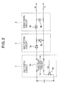
- FIG. 2 shows an example of the switching circuit, the rectifying circuit, and the smoothing circuit in FIG. 1 ;
- FIGS. 3( a ) to 3 ( c ) are time charts showing the pulse signal PS, the status of the load switching element 5 , and the load current IL;
- FIG. 4 is a flowchart showing the process for setting the PWE duty ratio, by means of a microcomputer used as the arithmetic processing circuit;
- FIGS. 5( a ) and 5 ( b ) are time charts showing the pulse signal PS and the waveform of the actual current IL flowing through the load;
- FIG. 6 is a time chart showing the pulsative current flowing through the load, with different values of the proportional gain PG;
- FIGS. 7( a ) to 7 ( c ) are time charts showing the pulse signal PS, the proportional gain PG, and the waveform of the load current IL according to the invention
- FIG. 8 is a flowchart showing the process of detecting a L-to-H change in the pulse signal, by means of a microcomputer
- FIG. 9( a ) shows the values of proportional gain stored as data in memory locations of different addresses in a memory area
- FIG. 9( b ) shows the values of integral gain stored as data in memory locations of different addresses in a memory area
- FIG. 10 is a flowchart showing the process of setting the proportional and integral gains upon detection of L-to-H change of the pulse signal
- FIG. 11 is a block diagram showing an example of image display apparatus having a light source drivers each formed of the constant current switching power supply apparatus according to Embodiment 1;
- FIG. 12 is a block diagram showing an example of the light source driver in FIG. 11 ;
- FIGS. 13( a ) to 13 ( d ) are time charts showing the status of light emission by the light emitting elements and the drive currents supplied to the respective light emitting elements.
- FIG. 1 is a block diagram showing a constant current switching power supply apparatus according to Embodiment 1 of the present invention.
- the illustrated constant current switching power supply apparatus is for controlling a current flowing through a load, and comprises a switching circuit 1 , a rectifying circuit 2 , a smoothing circuit 3 , a load switching element 4 , a current detecting element, an analog-to-digital converter (ADC) 7 , and an arithmetic processing circuit B.
- ADC analog-to-digital converter
- the invention is suitable to a situation where the load 4 is formed of a light emitting element such as an LED or an LD.
- the invention however is not limited to such a situation, and the load 4 may for example be a resistor.
- a direct current (DC) voltage is applied to the switching circuit 1 .
- the switching circuit 1 performs switching (PWM) according to a PWM signal Sw, to generate an alternating (AC) voltage.
- the output voltage of the switching circuit 1 is supplied to the rectifying circuit 2 .
- the rectifying circuit 2 rectifies the AC voltage from the switching circuit 1 .
- the smoothing circuit 3 smoothes the output of the rectifying circuit 2 .
- the output of the smoothing circuit 3 is supplied to the load 4 .
- the switching element 5 and the current detecting element 6 are connected in series with the load 4 , and the series connection is connected between output terminals of the smoothing circuit 3 .
- the switching element 5 turns on or off the current flowing through the load 4 , according to the pulse signal PS supplied from a pulse generator 9 .
- the switching element 5 may be in the form of semiconductor switch, such as a MOSFET or bipolar transistor.
- the current detecting element 6 detects the current flowing through the load 4 .
- the current detecting element 6 converts the current value to a voltage value, and may comprise a shunt resistor, or a Hall element.
- the output of the current detecting element 6 is supplied to the ADC 7 . Where the output of the current detecting element 6 is relatively small, an amplifier may be inserted between the current detecting element 6 and the ADC 7 .
- the ADC 7 converts the current value detected by the current detecting element 6 from an analog value to a digital value.
- the output of the ADC 7 is supplied, as the current detection value Id, to the arithmetic processing circuit 8 .
- the pulse signal PS is supplied not only to the switching element 5 , but also to the arithmetic processing circuit 8 . Also supplied to the arithmetic processing circuit 8 is a current command signal Ic from an external control circuit 10 .
- the current command signal Ic designates the value of the current flowing through the load 4 .
- the arithmetic processing circuit 8 performs feedback control over the current IL supplied to the load 4 , using the current command signal Ic as a target value Ir, and based on the deviation of the current detection value Id from the target value Ir. For this purpose, a duty ratio is determined based on a value obtained by multiplying the difference of the detection value ID from the target value Ir, and a PWM signal Sw corresponding to the duty ratio is output.
- the arithmetic processing circuit 8 is formed of a microprocessor, such a microcomputer, or DSP (Digital Signal Processor).
- the switching circuit 1 turns on and off the DC current, according to the PWM signal output from the arithmetic processing circuit 8 , to generate an AC current corresponding to the duty ratio.
- the switching circuit 1 may, for example, formed of a forward-mode converter-type switching circuit of an insulation type using a transformer 1 a , as shown in FIG. 2 , and having a primary winding 1 c connected to the switching element 1 b , so that the current through the primary winding is turned on and off by the PWM signal Sw.
- a primary winding 1 c connected to the switching element 1 b , so that the current through the primary winding is turned on and off by the PWM signal Sw.
- the AC voltage induced in the secondary winding 1 d of the transformer 1 a is again converted to a DC voltage by the rectifying circuit 2 .
- the rectifying circuit 2 comprises, for example, diodes 2 a and 2 b , as shown in FIG. 2 .
- a current flows through the diode 2 a .
- a current flows through the diode 2 b .
- the output voltage from the rectifying circuit 2 is supplied to the smoothing circuit 3 where ripples are removed, and a smoothed DC voltage is thereby output.
- the smoothing circuit 3 may, for example, be formed of an inductor 3 a and a capacitor 3 b connected to form an inverted L network.
- the current flowing through the diode 2 a during the on period of the switching element 1 b flows through the inductor 3 a to charge the capacitor 3 b , and also flows through the load 4 , the switching element 5 , and the current detecting element 6 , to serve as a drive current of the load 4 .
- energy stored in the inductor 3 a and the capacitor 3 b is released so that a current flows through the load 4 , the switching element 5 , the current detecting element 6 , and the diode 2 b .
- the switching circuit 1 By turning on and off of the switching circuit 1 in this way, the combination of the switching circuit 1 , the rectifying circuit 2 and the smoothing circuit 3 is able to provide a continuous current to the load 4 . Accordingly, by the switching on and off of the load switching element 5 , the current flowing through the load 4 can be turned on and off.
- FIGS. 3( a ) to 3 ( c ) show the relationship between the pulse signal PS ( FIG. 3( a )), the status of the load switching element 5 ( FIG. 3( b )), and the current flowing through the load 4 (load current) IL ( FIG. 3( c )). It is assumed that the switching element 5 is on when the pulse signal PS is H (at High level), and the switching element 5 is off when the pulse signal PS is L (at Low level). If the pulse signal PS is H, a current flows through the load 4 , and if the pulse signal PS is L, no current flows through the load 4 . Thus, the load current IL is a pulsative current in synchronous with the pulse signal PS.
- the relationship between the frequency Fsw of the PWM signal for causing a stable pulsative current through the load 4 , the frequency Fp of the pulse signal PS, is that Fsw>>Fp (Fsw is sufficiently high compared with Fp; or Fp is sufficiently low compared with Fsw. For instance, Fsw is several tens of kHz or higher, while fp is several kHz or lower.
- the operation of the arithmetic processing circuit 8 is next described.
- the arithmetic processing circuit 8 performs arithmetic operation, such as PI (proportional and integral) control which is generally used in a feedback control.
- PI proportional and integral
- the operations in the steps ST 1 to ST 7 will next be described in succession.
- the series of steps shown in FIG. 4 are performed once per one operation cycle.
- step ST 1 the current detection value Id is read or sampled from the ADC 7 .
- step ST 2 the current command value Ic is set as a current target value Ir.
- step ST 3 the difference (deviation) of the current detection value Id from the current target value Ir is detected as an error ⁇ I.
- step ST 4 the product of the proportional gain (constant) PG and the error ⁇ I is obtained as a proportional error (also called “proportional term”).
- step ST 5 the product of the integral gain (constant) IG and the integral of the error ⁇ I is obtained as an integral error (also called “integral term”).
- the integral of the error ⁇ I is obtained by accumulation of the error ⁇ I, and accordingly, by the addition of the error ⁇ I at each sampling point (each cycle of operation), and the integral value (accumulation) up to the previous sampling point (previous cycle of operation).
- the proportional error and the integral error are added to determine PI value.
- the PI value is scaled with an appropriate value (i.e., multiplied by a coefficient), to determine the duty ratio of the PWM signal Sw.
- the process described above is carried out periodically, in synchronism with the carrier signal having the same frequency as the PWM signal Sw, or at an interval set by the internal timer in the microcomputer.
- the PWM signal Sw produced based on the result of the arithmetic processing is sent from the arithmetic processing circuit 8 to the switching circuit 1 .
- the load current IL is shown to have an ideal pulsative waveform. In practice, however, the load current may have a waveform as shown in FIG. 5( b ). That is, when the pulse signal PS ( FIG. 5( a )) turns on the switching element 5 , the current begins to flow, and a certain period (rise time) is required before the current is stabilized at a certain constant value. This is because it takes time before the power supply apparatus responds after the current begins to flow through the load 4 . When the current falls, there is no such a delay, because the switching element 5 is turned off to interrupt the current.
- the relationship between the pulsative current flowing through the load 4 and the value of the proportional gain PG is shown in FIG. 6 .
- the rising waveform With a larger value of the proportional gain PG, the rising waveform becomes sharper (the rise time becomes shorter), but an overshooting occurs before the current value settles at a constant value.
- the rising waveform With an even larger proportional gain, the rising waveform becomes even sharper (the rise time becomes even shorter), and the current is not stabilized at a constant value, but oscillates about the target value.
- the value of the proportional gain PG is varied with time.
- the relationship between the pulse signal PS, the proportional gain PG, and the waveform of the load current IL according to the present invention is shown in FIGS. 7( a ) to 7 ( c ).
- the proportional gain PG ( FIG. 7( b )) is set to a first predetermined value PGm when the pulse signal PS ( FIG. 7( a )) is changed from L to H, and is thereafter reduced gradually with time until it reaches a second predetermined value PGs.
- the proportional gain PG is set to a large value only at the time of rising of the load current IL ( FIG.
- the proportional gain PG is set to a relatively small value PGs after the load current approaches the target value Ir, so that the oscillation of the load current IL about the target value Ir is prevented.
- the ultimate value PGs of the proportional gain PG is set sufficiently small such that, when the load current IL approaches the target value Ir, the load current IL does not oscillate. In other words, the ultimate value PGs is an optimum value in a steady state of the load current.
- FIG. 8 shows a pulse signal detection flow.
- step ST 11 judgment is made as to whether the pulse signal PS has changed from L to H.
- step ST 12 time t (as a parameter) is initialized to “0”.
- the pulse signal PS is supplied to the I/O terminal, or an interrupt terminal 8 a of the microcomputer, so that, by means of I/O polling process, or interrupt process, the microcomputer, can detects the timing at which the pulse signal PS changes from L to H, i.e., the timing at which the switching element is turned on (is changed from off to on).
- F(t) is not limited to any specific one, but, in order to reduce the time required for arithmetic operation, F(t) may be one defining the following relationship.
- the value of t is assumed to be increased by one every predetermined unit time.
- the “predetermined time” is for instance the time interval at which the arithmetic operation is performed, or the cycle of operation illustrated in FIG. 4 .
- PG is given by PGs multiplied by a power of two, as in the above example, and the value of time t is increased by “1” at every time interval of the arithmetic operation, the value of PG can be easily obtained by adding 1 to t at every arithmetic operation, and bit-shifting the current value to the right by one bit.
- the gain in the PI control performed by the arithmetic processing circuit 8 in particular the proportional gain PG is set to a relatively large value (first predetermined value) immediately after the switching element 5 is changed from the off state to the on state, and then gradually made smaller with elapse of time.
- first predetermined value a relatively large value immediately after the switching element 5 is changed from the off state to the on state
- the integral gain IG is assumed to be constant. However, it may be desirable that the integral gain IG is also varied, depending on the time constant of the smoothing circuit 3 , the stray inductance and stray capacitance on the printed circuit board, and the current-voltage characteristic of the load 4 . In such a case, in the same way as the above description, it is also desirable that the proportional gain PG is set to a relatively large value (first predetermined value which is larger than the value (second predetermined value) used in a steady state), and is gradually made smaller with time. On the other hand, it is desirable that integral gain IG be optimized through observation of the current waveform in connection with the each apparatus used, rather than using a predefined relationship with time. However, the gain may vary in a predefined pattern with the time having elapsed from the time when the switching element 4 is changed from off to on.
- a plurality of values of the proportional gain PG are stored in advance in the memory 8 b or 11 , at a plurality of memory locations designated by the addresses which are associated with different values of the time having elapsed after the off-to-on change of the switching element 5 , and, in performing the feedback control, the value of the proportional gain is read from the memory location associated with (corresponding to) the current time having elapsed after the off-to-on change of the switching element 5 .
- a plurality of values of the integral gain are stored in advance in the memory 8 b or 11 , at memory locations designated by the addresses associated with different values of the time after the off-to-on change of the switching element 5 , and, in performing the feedback control, the value of the integral gain is read from the memory location associated with (corresponding to) the current time having elapsed after the off-to-on change of the switching element 5 .
- the values of the gains thus read are used for arithmetic operation of PI control in the arithmetic processing circuit 8 .
- FIG. 9( a ) shows an example of the relationship between the plurality of addresses n, n+1, n+2, . . . of the memory locations in a region of the memory 8 b or 11 storing the values of the proportional gain, and the values PG 0 , PG 1 , PG 2 , . . . of the proportional gain PG stored in the respective memory locations.
- FIG. 9( b ) shows an example of the relationship between the plurality of addresses m, m+1, m+2, . . . of the memory locations in a region of the memory 8 b or 11 storing the values of the integral gain, and the values IG 0 , IG 1 , IG 2 , . . . of the integral gain IG stored in the respective memory locations.
- the data PG 0 and IG 0 at the memory locations designated by the initial value (n in FIG. 9( a ) and m in FIG. 9( b )) of the memory address are read. Thereafter, the memory address is incremented by one at every time interval, or each time an arithmetic operation is performed, and data is read from the incremented address and used as the gain.
- the data PG 0 associated with the initial value n of the memory address shown in FIG. 9( a ) corresponds to PGm shown in FIG. 7 .
- the data PG 1 , PG 2 , . . . associated with the addresses m+1, m+2, . . . have such a relation that its value is decreased with the increase of the address value (corresponding to the time having elapsed).
- FIG. 10 shows a flow for detecting a pulse signal.
- step ST 11 judgment is made as to whether the pulse signal PS has changed from L to H.
- step ST 13 the proportional gain address is set to the initial value n, and the integral gain address is set to the initial value m.
- the addresses (of the memory locations from which the gains are read) are returned to the initial values n, and m, respectively, and each time the arithmetic operation is performed, “1” is added to each of the addresses, and the gains are read from the memory locations of the addresses (after the addition of “1”).
- the values of the gains can thus be changed with time, in synchronism with the pulse signal PS.
- the capacity of the memory need not be so large, and may have about 10 addresses for each gain, since it is up to the time when the load current reaches a predetermined value, after the rise, that the values of the gains are required.
- the proportional gain PG and the integral gain IG are both varied with time.
- a memory similar to that used in the above example may be used where the integral gain IG may be held constant, and only the proportional gain PG is varied with time. In such a case, only the memory for storing the proportional gain PG is required, and the memory for storing the integral gain IG may be omitted.
- FIG. 11 shows an example of an image display apparatus having a light source driving apparatus formed of a constant current switching power supply apparatus described in connection with Embodiment 1.
- the illustrated image display apparatus comprises a receiver 19 , a video data processor 20 , a timing controller 21 , a spatial modulator controller 22 , a spatial modulator controller 22 , a light source unit 23 , optical fibers 25 , a light pipe 26 , a lens 27 , a light valve 28 , a lens 29 , and a screen 30 .
- the light source unit 23 has light emitting elements 4 R, 4 G, and 4 B, and a light source driver 24 .
- the light emitting elements 4 R, 4 G, and 4 B correspond to the load 4 in Embodiment 1.
- Video data VD 1 and a synchronous signal SY are supplied from an external image equipment, to the receiver 19 .
- the video data VD 1 is supplied from the receiver 19 to the video data processor 20 .
- the video data VD 2 processed in the video data processor 20 is input to the spatial modulator controller 22 .
- the synchronous signal SY received by the receiver 19 is supplied as a timing signal TS 1 to the timing controller 21 .
- the timing controller 21 supplies a timing signal TS 2 to the spatial modulator controller 22 , and also supplies a timing signal TS 3 (including signals TS 3 r , TS 3 g , TS 3 b ) to the light source driver 24 of the light source unit 23 .
- the spatial modulator controller 22 supplies video data VD 3 for displaying an image, to the light valve 28 .
- the light source driver 24 supplies currents ILr, ILg and ILb necessary to drive the light emitting elements 4 R, 4 G, and 4 B.
- Each of the light emitting elements 4 R, 4 G, and 4 B may be formed of an LED or an LD. In the description of the present embodiment, it is assumed that the light emitting elements are assumed to be formed of an LD.
- Three beams of light emitted from the red LD 4 R, the green LD 4 G, and the blue LD 4 B are passed through the optical fibers 25 , the light pipe 26 , and the lens 27 , and are spatially modulated by the light valve 28 , and passed through the lens 29 , and reach the screen 30 .
- FIG. 12 shows an example of configuration of the light source driver 24 .
- the illustrated light source driver 24 comprises a red light source driving unit 24 r , a green light source driving unit 24 g , and a blue light source driving unit 24 b .
- Each of the driving units 24 r , 24 g and 24 b is formed of the switching power supply apparatus shown in FIG. 1 , and each of the red LD 4 R, the green LD 4 G, and the blue LD 4 B corresponds to the load 4 shown in FIG. 1 .
- Each of the light source driving unit 24 r , the green light source driving unit 24 g , and the blue light source driving unit 24 b receives, as a timing signal TS 3 r , TS 3 g or TS 3 b , a signal corresponding to the pulse signal PS shown in FIG. 1 .
- a DC voltage Vdc obtained by conversion from the commercial power supply, by means of an AC/DC converter within the image display apparatus is supplied to the light source driving unit 24 r , the green light source driving unit 24 g , and the blue light source driving unit 24 b .
- the DC voltage Vdc in FIG. 12 serves as the DC voltage in FIG. 1 .
- Current command values Icr, Icg and Icb each of which corresponds to the current command value Ic shown in FIG. 1 may be supplied from the control circuit 12 within the image display apparatus, as illustrated, or may be set in advance within each of the light source driving units.
- the video data VD 1 received by the receiver 19 is supplied to the video data processor 20 .
- the synchronous signal SY received by the receiver 19 is supplied as the timing signal TS 1 to the timing controller 21 .
- the timing controller 21 supplies the timing signals TS 2 and TS 3 to the spatial modulator controller 22 and the light source driver 24 , such that the supply of the video data VD 3 from the spatial modulator controller 22 to the light valve 28 , and the driving of the red LD 4 R, green LD 4 G, and blue LD 4 B by the light source driver 24 are in synchronous with each other.
- the video data processor 20 performs processing on the video data VD 1 supplied from the receiver 19 , so as to produce video data VD 2 suitable for driving the light valve 28 , and the video data VD 2 obtained by the processing is supplied to the spatial modulator controller 22 .
- the spatial modulator controller 22 supplies the video data VD 2 to the light valve 28 , in accordance with the timing signal TS 2 supplied from the timing controller 21 .
- the light source driver 24 drives the red LD 4 R, the green LD 4 G, and the blue LD 4 B (forming the light emitting elements) in accordance with the timing signal TS 3 output from the timing controller 2 .
- the three LDs 4 R, 4 G and 4 B emit light sequentially, in accordance with the drive timing.
- the light beams emitted from the red LD 4 R, the green LD 4 G, and the blue LD 4 B are passed through the optical fibers 25 , and made to converge by the light pipe 26 , into a single beam, and the light of the single beam is passed through the lens 27 , and illuminates the light valve 28 .
- the light valve 28 spatially modulates the light beam, in accordance with the video data VD 2 .
- the light beam modulated by the light valve 28 is passed through the lens 29 , and reaches the screen 30 .
- the light beam spatially modulated by the light valve 28 is projected on the screen 30 , and displayed as an image.
- FIGS. 13( a ) to 13 ( d ) show the relationship between the status of the light emission by the red LD 4 R, the green LD 4 G, and the blue LD 4 B, and the drive currents.
- the red LD 4 R, the green LD 4 G, and the blue LD 4 B are driven by the light source driver 24 , sequentially in a time-division manner, in accordance with the timing signal TS 3 supplied from the timing controller 21 , as shown in FIGS. 13( b ) to 13 ( d ).
- a red light beam, a green light beam, and a blue light beam are emitted sequentially as shown in FIG. 13( a ).
- Video data of the respective colors are supplied from the optical modulator controller 22 to the light valve 28 , in time with the drive periods of the respective light emitting elements, and the image corresponding to the video data of the respective colors are displayed in a time-division manner, on the screen 30
- the images are sequentially displayed in a time-division manner. Because the switching between images of different colors in the display is at a high rate, the viewer sees the images as a color image, without unpleasant feeling because of the persistence effects of the eyes.
- the maximum luminance of the image displayed on the screen 30 in the image display apparatus described above is brighter as the integral of the strength of the light emission over the time during each time slot in the time division drive is larger. Accordingly, it is important that the light emitting elements emit as strong a light as possible in a given light emitting period. Accordingly, it is necessary to shorten the rise time of the light emission waveform, i.e., the rise time of the drive current.
- the constant current switching power supply apparatus is used as each of the light source driving units 24 r , 24 g , and 24 b , and if the proportional gain PG for the light source driving unit is initially set to a relatively large value (first predetermined value), in synchronism with the timing signal TS 3 , and is then gradually reduced with time, it is possible to shorten the rise time of the drive current of each light emitting element.
- the value of the proportional gain PG for the light source driving units 24 r , 24 g and 24 b used in the light source driver 24 is made to be relatively large (first predetermined value), in synchronism with the timing signal, and then made to be reduced gradually. In this way, it is possible to shorten the rise time of the drive current of each of the light emitting elements 4 R, 4 G, and 4 B. As a result, the luminance of the image display apparatus is increased.
- the values of the gains may be stored in a memory in advance, and may be read in synchronism with the timing signal TS 3 , from different memory locations designated by addresses which are incremented with time.
- the values of the gains for the light source driving units 24 r , 24 g and 24 b may be different from each other.
Landscapes
- Engineering & Computer Science (AREA)
- Power Engineering (AREA)
- Circuit Arrangement For Electric Light Sources In General (AREA)
- Led Devices (AREA)
- Control Of Voltage And Current In General (AREA)
- Dc-Dc Converters (AREA)
- Semiconductor Lasers (AREA)
- Projection Apparatus (AREA)
Abstract
Description
PG=23 ×PGs when t=0;
PG=22 ×PGs when t=1;
PG=21 ×PGs when t=2,
PG=20 ×PGs when t≧3.
Claims (9)
Applications Claiming Priority (2)
| Application Number | Priority Date | Filing Date | Title |
|---|---|---|---|
| JP2008-213714 | 2008-08-22 | ||
| JP2008213714A JP2010049523A (en) | 2008-08-22 | 2008-08-22 | Constant current switching power supply device, method of driving the same, light source drive device, method of driving the same, and image display device |
Publications (2)
| Publication Number | Publication Date |
|---|---|
| US20100045195A1 US20100045195A1 (en) | 2010-02-25 |
| US8148906B2 true US8148906B2 (en) | 2012-04-03 |
Family
ID=41695727
Family Applications (1)
| Application Number | Title | Priority Date | Filing Date |
|---|---|---|---|
| US12/536,840 Expired - Fee Related US8148906B2 (en) | 2008-08-22 | 2009-08-06 | Constant current switching power supply apparatus, method of driving it, light source driving apparatus, method of driving it, and image display apparatus |
Country Status (2)
| Country | Link |
|---|---|
| US (1) | US8148906B2 (en) |
| JP (1) | JP2010049523A (en) |
Cited By (2)
| Publication number | Priority date | Publication date | Assignee | Title |
|---|---|---|---|---|
| US20120161654A1 (en) * | 2010-12-27 | 2012-06-28 | Sanken Electric Co., Ltd. | Constant current power supply device |
| US20170085184A1 (en) * | 2015-09-18 | 2017-03-23 | Joint Power Exponent, Ltd. | Converter control system |
Families Citing this family (17)
| Publication number | Priority date | Publication date | Assignee | Title |
|---|---|---|---|---|
| JP2011098494A (en) * | 2009-11-05 | 2011-05-19 | Sharp Corp | Optical scanner, and image forming apparatus with the optical scanner |
| DE102010003136A1 (en) * | 2010-03-23 | 2011-09-29 | Osram Gesellschaft mit beschränkter Haftung | Circuit arrangement and method for operating at least one LED |
| JP5910148B2 (en) * | 2012-02-17 | 2016-04-27 | カシオ計算機株式会社 | Drive device, blinking device, and projection device |
| JP6206757B2 (en) * | 2013-08-02 | 2017-10-04 | パナソニックIpマネジメント株式会社 | Lighting apparatus and lighting device used therefor |
| JP2015050787A (en) | 2013-08-30 | 2015-03-16 | カシオ計算機株式会社 | Drive device, light emitting device, projection device, control method, and storage medium |
| JP2016181544A (en) | 2015-03-23 | 2016-10-13 | ファナック株式会社 | Constant current control power supply and laser oscillator |
| JP2017059825A (en) * | 2015-09-15 | 2017-03-23 | パナソニックIpマネジメント株式会社 | Semiconductor light source driving device and projection type video display device |
| JP6642144B2 (en) * | 2016-03-11 | 2020-02-05 | コニカミノルタ株式会社 | Power supply control device and image forming apparatus |
| CN106102221B (en) * | 2016-06-16 | 2017-10-03 | 厦门印天电子科技有限公司 | A kind of LED light adjusting circuits |
| US10728976B2 (en) | 2018-05-15 | 2020-07-28 | Robern, Inc. | LED control method for perceived mixing |
| JP7162243B2 (en) | 2018-10-16 | 2022-10-28 | パナソニックIpマネジメント株式会社 | Semiconductor light source driving device and projection type image display device |
| JP6886450B2 (en) | 2018-11-30 | 2021-06-16 | コイト電工株式会社 | Power adjustment system |
| JP7181805B2 (en) * | 2019-02-12 | 2022-12-01 | 株式会社三社電機製作所 | Power supply circuit for transient thermal resistance measurement of semiconductor devices |
| JP7147632B2 (en) * | 2019-03-01 | 2022-10-05 | 株式会社デンソー | LED drive circuit |
| JP7594433B2 (en) * | 2020-12-24 | 2024-12-04 | 株式会社三社電機製作所 | Laser diode power supply unit |
| JP7594449B2 (en) * | 2021-01-27 | 2024-12-04 | 株式会社三社電機製作所 | Laser diode power supply unit |
| JP7550722B2 (en) * | 2021-06-07 | 2024-09-13 | 株式会社遠藤照明 | Lighting and power supplies |
Citations (5)
| Publication number | Priority date | Publication date | Assignee | Title |
|---|---|---|---|---|
| JP2005142137A (en) | 2003-10-15 | 2005-06-02 | Matsushita Electric Works Ltd | LED lighting device |
| JP2007065677A (en) | 1997-03-24 | 2007-03-15 | Sony Corp | Video display device |
| US20080024526A1 (en) * | 2006-07-28 | 2008-01-31 | Chun-Seok Ko | Organic light emitting diode display and driving method thereof |
| US20080238340A1 (en) * | 2007-03-26 | 2008-10-02 | Shun Kei Mars Leung | Method and apparatus for setting operating current of light emitting semiconductor element |
| US20090085489A1 (en) * | 2007-09-28 | 2009-04-02 | Chunghwa Picture Tubes, Ltd. | Circuit and method for driving and controling light source |
-
2008
- 2008-08-22 JP JP2008213714A patent/JP2010049523A/en not_active Withdrawn
-
2009
- 2009-08-06 US US12/536,840 patent/US8148906B2/en not_active Expired - Fee Related
Patent Citations (6)
| Publication number | Priority date | Publication date | Assignee | Title |
|---|---|---|---|---|
| JP2007065677A (en) | 1997-03-24 | 2007-03-15 | Sony Corp | Video display device |
| JP2005142137A (en) | 2003-10-15 | 2005-06-02 | Matsushita Electric Works Ltd | LED lighting device |
| US20080024526A1 (en) * | 2006-07-28 | 2008-01-31 | Chun-Seok Ko | Organic light emitting diode display and driving method thereof |
| US20080238340A1 (en) * | 2007-03-26 | 2008-10-02 | Shun Kei Mars Leung | Method and apparatus for setting operating current of light emitting semiconductor element |
| US20090085489A1 (en) * | 2007-09-28 | 2009-04-02 | Chunghwa Picture Tubes, Ltd. | Circuit and method for driving and controling light source |
| US8035310B2 (en) * | 2007-09-28 | 2011-10-11 | Chunghwa Picture Tubes, Ltd. | Circuit for driving light source |
Cited By (4)
| Publication number | Priority date | Publication date | Assignee | Title |
|---|---|---|---|---|
| US20120161654A1 (en) * | 2010-12-27 | 2012-06-28 | Sanken Electric Co., Ltd. | Constant current power supply device |
| US8547028B2 (en) * | 2010-12-27 | 2013-10-01 | Sanken Electric Co., Ltd. | Constant current power supply device |
| US20170085184A1 (en) * | 2015-09-18 | 2017-03-23 | Joint Power Exponent, Ltd. | Converter control system |
| US9847726B2 (en) * | 2015-09-18 | 2017-12-19 | Joint Power Exponent, Ltd. | Converter control system |
Also Published As
| Publication number | Publication date |
|---|---|
| US20100045195A1 (en) | 2010-02-25 |
| JP2010049523A (en) | 2010-03-04 |
Similar Documents
| Publication | Publication Date | Title |
|---|---|---|
| US8148906B2 (en) | Constant current switching power supply apparatus, method of driving it, light source driving apparatus, method of driving it, and image display apparatus | |
| US9235109B2 (en) | Light source driving device, light source driving method, and image display device | |
| JP4833754B2 (en) | LED drive circuit for backlight having constant current control function | |
| US8217584B2 (en) | Driving circuit for driving light emitting diodes and dimmer | |
| US20110025225A1 (en) | Light-Emitting Diode Driver Circuit and Lighting Apparatus | |
| US8049436B2 (en) | Dimmer and lighting apparatus | |
| US9167647B1 (en) | Control circuit and control method for dimming a lighting device | |
| JP5959785B2 (en) | Power supply device, light source lighting device, and battery charging device | |
| US9852680B2 (en) | Projection type display device and method for controlling operation of projection type display device | |
| EP2672784B1 (en) | Constant current control buck converter without current sense | |
| EP3491891B1 (en) | Dimming led circuit augmenting dc/dc controller integrated circuit | |
| KR20160020868A (en) | Power supply, power control method thereof, and display apparatus having the same | |
| JP2007080819A (en) | Display device and control method thereof | |
| US20100033102A1 (en) | Light Adjusting Device for a Light Emitting Diode and Related Light Adjusting Method and Light Emitting Device | |
| CN100474208C (en) | Led driving apparatus and method of controlling luminous power | |
| JP5077593B2 (en) | Discharge lamp lighting device, projector, and control method of discharge lamp lighting device | |
| KR101864466B1 (en) | Power supply device | |
| KR20130015720A (en) | Backlight unit, control apparatus and control method thereof | |
| JP2008159329A (en) | Power supply device for discharge lamp and control method thereof | |
| JP2006060009A (en) | Driving circuit for light-emitting diode | |
| JP7510114B2 (en) | Lighting devices and lighting fixtures | |
| JP2020027751A (en) | Lighting device and lighting apparatus using the same | |
| JP2008295167A (en) | Constant current switching power supply device and light source device | |
| JP7155976B2 (en) | lighting equipment | |
| US20120146528A1 (en) | Circuit Configuration for Operating LEDS for a Micromirror Arrangement |
Legal Events
| Date | Code | Title | Description |
|---|---|---|---|
| AS | Assignment |
Owner name: MITSUBISHI ELECTRIC CORPORATION,JAPAN Free format text: ASSIGNMENT OF ASSIGNORS INTEREST;ASSIGNORS:YAMAMURO, TAKAHIKO;NAGASE, AKIHIRO;OKAZAKI, KOUJI;REEL/FRAME:023074/0815 Effective date: 20090713 Owner name: MITSUBISHI ELECTRIC CORPORATION, JAPAN Free format text: ASSIGNMENT OF ASSIGNORS INTEREST;ASSIGNORS:YAMAMURO, TAKAHIKO;NAGASE, AKIHIRO;OKAZAKI, KOUJI;REEL/FRAME:023074/0815 Effective date: 20090713 |
|
| REMI | Maintenance fee reminder mailed | ||
| LAPS | Lapse for failure to pay maintenance fees | ||
| STCH | Information on status: patent discontinuation |
Free format text: PATENT EXPIRED DUE TO NONPAYMENT OF MAINTENANCE FEES UNDER 37 CFR 1.362 |
|
| FP | Expired due to failure to pay maintenance fee |
Effective date: 20160403 |