US8098224B2 - Driver circuit for display device and display device - Google Patents
Driver circuit for display device and display device Download PDFInfo
- Publication number
- US8098224B2 US8098224B2 US11/052,789 US5278905A US8098224B2 US 8098224 B2 US8098224 B2 US 8098224B2 US 5278905 A US5278905 A US 5278905A US 8098224 B2 US8098224 B2 US 8098224B2
- Authority
- US
- United States
- Prior art keywords
- signal
- precharge
- circuit
- lines
- switches
- Prior art date
- Legal status (The legal status is an assumption and is not a legal conclusion. Google has not performed a legal analysis and makes no representation as to the accuracy of the status listed.)
- Expired - Fee Related, expires
Links
Images


Classifications
-
- H—ELECTRICITY
- H04—ELECTRIC COMMUNICATION TECHNIQUE
- H04M—TELEPHONIC COMMUNICATION
- H04M1/00—Substation equipment, e.g. for use by subscribers
- H04M1/02—Constructional features of telephone sets
- H04M1/0202—Portable telephone sets, e.g. cordless phones, mobile phones or bar type handsets
- H04M1/0206—Portable telephones comprising a plurality of mechanically joined movable body parts, e.g. hinged housings
- H04M1/0208—Portable telephones comprising a plurality of mechanically joined movable body parts, e.g. hinged housings characterized by the relative motions of the body parts
- H04M1/0235—Slidable or telescopic telephones, i.e. with a relative translation movement of the body parts; Telephones using a combination of translation and other relative motions of the body parts
- H04M1/0237—Sliding mechanism with one degree of freedom
-
- G—PHYSICS
- G09—EDUCATION; CRYPTOGRAPHY; DISPLAY; ADVERTISING; SEALS
- G09G—ARRANGEMENTS OR CIRCUITS FOR CONTROL OF INDICATING DEVICES USING STATIC MEANS TO PRESENT VARIABLE INFORMATION
- G09G3/00—Control arrangements or circuits, of interest only in connection with visual indicators other than cathode-ray tubes
- G09G3/20—Control arrangements or circuits, of interest only in connection with visual indicators other than cathode-ray tubes for presentation of an assembly of a number of characters, e.g. a page, by composing the assembly by combination of individual elements arranged in a matrix no fixed position being assigned to or needed to be assigned to the individual characters or partial characters
- G09G3/34—Control arrangements or circuits, of interest only in connection with visual indicators other than cathode-ray tubes for presentation of an assembly of a number of characters, e.g. a page, by composing the assembly by combination of individual elements arranged in a matrix no fixed position being assigned to or needed to be assigned to the individual characters or partial characters by control of light from an independent source
- G09G3/36—Control arrangements or circuits, of interest only in connection with visual indicators other than cathode-ray tubes for presentation of an assembly of a number of characters, e.g. a page, by composing the assembly by combination of individual elements arranged in a matrix no fixed position being assigned to or needed to be assigned to the individual characters or partial characters by control of light from an independent source using liquid crystals
- G09G3/3611—Control of matrices with row and column drivers
- G09G3/3685—Details of drivers for data electrodes
- G09G3/3688—Details of drivers for data electrodes suitable for active matrices only
-
- G—PHYSICS
- G09—EDUCATION; CRYPTOGRAPHY; DISPLAY; ADVERTISING; SEALS
- G09G—ARRANGEMENTS OR CIRCUITS FOR CONTROL OF INDICATING DEVICES USING STATIC MEANS TO PRESENT VARIABLE INFORMATION
- G09G2310/00—Command of the display device
- G09G2310/02—Addressing, scanning or driving the display screen or processing steps related thereto
- G09G2310/0243—Details of the generation of driving signals
- G09G2310/0248—Precharge or discharge of column electrodes before or after applying exact column voltages
Definitions
- the present invention relates to a driver circuit that precharges signal supply lines of a display device before supplying signals thereto, and relates to a display device.
- an active matrix liquid crystal display device which performs dot sequential driving, precharges signal lines before supplying video signals to pixels through data signal lines. This makes it possible to charge the pixels by predetermined amounts stably.
- a precharge power source in order to adopt a driving method in which all signal lines are precharged simultaneously (hereinafter “simultaneous precharge method”), a precharge power source must have high driving capability. This is because the sum of wire capacity of all signal lines is large.
- there is a driving method in which precharge is performed unit by unit, each unit including a small number of signal lines hereinafter “sequential precharge method”.
- Patent Publication 1 Japanese Publication for Laid-Open Patent Application, Tokukaihei 7-295520; corresponding to U.S. Pat. No. 5,686,936 discloses an arrangement in which, in outputting a video signal to one data signal line, a switch of another data signal line is turned ON by using a video-signal-sampling signal outputted from a shift register of a data signal line driver, so as to perform precharge by using a precharge power source.
- Patent Publication 2 Japanese Publication for Laid-Open Patent Application, Tokukai 2000-89194; corresponding to U.S. Pat. No. 6,731,266B1 discloses an arrangement in which all data signal lines are divided onto several blocks including data signal lines, and, in outputting video signals from a data signal line driver to data signal lines of an n-th data signal line block, data signal lines of an (n+1)-th data signal line block are precharged by a precharge power source by using video-signal-sampling signals.
- Patent Publication 3 Japanese Publication for Laid-Open Patent Application, Tokukai 2000-206491 discloses an arrangement in which a transfer pulse input of each transfer stage of a data signal line driver is used as a timing pulse for opening or closing an analog switch for precharging the data signal line of the transfer stage and also used, by being delayed from the timing pulse for precharge, as a timing pulse for opening or closing an analog switch for outputting substantive data (video signal) to the data signal line.
- a transfer pulse output of the transfer stage is used as a transfer pulse input of a next transfer stage, and as a timing pulse for precharge and a timing pulse for substantive data output of the next transfer stage.
- each data signal line is provided with a switch having a capacitor-type control terminal (e.g. a gate) such as MOSFET including a TFT, and the switch is switched dot sequentially between conductive and nonconductive by controlling the charge voltage of the control terminal.
- a control signal for dot sequentially switching the switch is outputted after being shifted in a horizontal direction by a shift register generally including plural stages of flip-flops.
- a similar switch, which is switched dot sequentially between conductive and nonconductive so as to precharge the data signal lines, is provided separately.
- a circuit for performing precharge is provided inside the data signal line driver, so that the frame of the liquid crystal display device has sufficient area, for example. As a result, the area of the precharge circuit can be reduced.
- Patent Publication 4 Japanese Publication for Laid-Open Patent Application, Tokukai 2001-135093; corresponding to U.S. Pat. No. 6,724,361B1
- Patent Publication 5 Japanese Publication for Laid-Open Patent Application, Tokukai 2001-307495; corresponding to U.S. Pat. No.
- Patent Publication 6 Japanese Publication for Laid-Open Patent Application, Tokukai 2000-339985
- Japanese Publication 6 Japanese Publication for Laid-Open Patent Application, Tokukai 2000-339985
- Japanese Publication 6 Japanese Publication for Laid-Open Patent Application, Tokukai 2000-339985
- Patent Publication 7 (U.S. Patent Application Publication, No. 023461/2003), which is a publication for a laid-open patent application filed by the applicant of the present invention, discloses an arrangement of providing a precharge circuit and a shift register. While write signals are written by a write circuit onto a part of signal supply lines, the precharge circuit precharges the rest of the signal supply lines.
- the shift register includes a control signal supply circuit for outputting a precharge control signal, which controls conductivity (conductive or non conductive) of a second switch, to a second control terminal through a second signal line, which is separated from a first signal line for transmitting the timing pulse to a first control terminal.
- FIG. 27 illustrates driving waveforms in a normal scanning state (in which a video signal is supplied to each source bus line) of a display device that precharges a plurality of source bus lines by the conventional simultaneous precharge method.
- the driving waveforms are those of three adjacent source bus lines SL 1 , SL 2 , and SL 3 .
- SSP is a start pulse of the source
- SCK is a source clock signal
- PCTL is a precharge instruction signal instructing the timing for performing simultaneous precharge of the source bus lines.
- SMP 1 , SMP 2 , and SMP 3 are sampling timing signals instructing the timing for sampling the video signals to the three adjacent source bus lines SL 1 to SL 3 , respectively.
- VSL 1 , VSL 2 , and VSL 3 are potentials of the source bus lines SL 1 to SL 3 , respectively.
- Operation for precharge is as follows.
- the precharge instruction signal PCTL is effective (is High) and precharge potentials are supplied to the source bus lines SL 1 to SL 3 , respectively.
- the start pulse SSP transition to High
- scanning at a speed in accordance with the clock signal SCK is started, and video signals are supplied to the source bus lines SL 1 to SL 3 in accordance with the sampling timing signals SMP 1 to SMP 3 , respectively.
- the simultaneous precharge method for example, in order to fix the potentials of the source bus lines to a desired potential when scanning is suspended, control is performed so that precharge is performed in accordance with the instruction signal PCTL during t 7 to t 8 .
- the precharge instruction signal is High during a period from t 1 to t 2 , which is before periods from t 3 to t 6 for supplying video signals to the source bus lines SL 1 to SL 3 , and during a period from t 7 to t 8 , which is after periods from t 3 to t 6 for supplying video signals.
- precharge potentials are respectively supplied to the source bus lines SL 1 to SL 3 during the period from t 1 to t 2 and the period from t 7 to t 8 . That is, during the periods in which video signals are not supplied to the source bus lines SL 1 to SL 3 , the source bus lines SL 1 to SL 3 are precharged simultaneously. As a result, the potentials of the source bus lines SL 1 to SL 3 are always kept to be not lower than a desired potential. Thus, in the simultaneous precharge method, it is possible to supply precharge potentials to the source bus lines even when scanning is suspended.
- FIG. 29 illustrates a normal scanning state of the case in which the sequential precharge method is adopted.
- the sequential precharge method precharge potentials are supplied sequentially to the source bus lines in the normal scanning state of FIG. 29 .
- Patent Publication 4 to 6 have no disclosure or suggestion concerning precharge.
- An object of the present invention is therefore to provide a driver circuit that can precharge signal supply lines of a display device sufficiently even with a precharge power source having relatively low driving capability, and to provide a display device using the driver circuit.
- a driver circuit for a display devise in accordance with the present invention is a driver circuit for a display device including a plurality of signal supply lines, the driver circuit including: a write circuit for writing write signals onto the signal supply lines line by line or by units of lines; and a precharge circuit for precharging the signal supply lines, while a write signal is written by the write circuit onto a signal supply line, the precharge circuit precharging another signal supply line, and, while no write signal is written by the write circuit onto any of the signal supply lines, the precharge circuit precharging the signal supply lines simultaneously.
- the precharge circuit precharges another signal supply line, and, while no write signal is written by the write circuit onto any of the signal supply lines, the precharge circuit precharges the signal supply lines simultaneously.
- precharge is performed for a longer time than in a case in which precharge is performed only while writing of write signals onto signal supply lines is suspended or a case in which, while a write signal is written by the write circuit onto a signal supply line, another signal supply line is precharged. As a result, it is possible to precharge the signal supply lines sufficiently.
- the amount of charge that should be supplied to the signal supply lines while the writing of write signals onto the signal supply lines is suspended is smaller than in a case in which precharge is performed only while the writing of write signals onto the signal supply lines is suspended. As a result, it is possible to precharge the signal supply lines even with a precharge power source having relatively low driving capability.
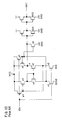
- FIG. 1 is a circuit block diagram illustrating an arrangement of a data signal line driver of a first embodiment of the present invention.
- FIG. 2 is a circuit diagram illustrating an arrangement of an example of a switching circuit.
- FIG. 3 is a timing chart illustrating signals associated with operation of the data signal line driver of FIG. 1 .
- FIG. 4 is a figure relating to the data signal line driver of FIG. 1 , illustrating a timing chart of each signal and potentials of source bus lines while scanning is suspended and while scanning is performed.
- FIG. 5 is a circuit block diagram illustrating an arrangement of a variation example of the data signal line driver of FIG. 1 .
- FIG. 6 is a circuit block diagram illustrating an arrangement of a data signal line driver of a second embodiment of the present invention.
- FIG. 7 is a timing chart illustrating signals associated with operation of the data signal line driver of FIG. 6 .
- FIG. 8 is a circuit block diagram illustrating an arrangement of a variation example of the data signal line driver of FIG. 6 .
- FIG. 9 is a circuit block diagram illustrating an arrangement of a data signal line driver of a third embodiment of the present invention.
- FIG. 10 is a circuit diagram illustrating an arrangement of an example of the level shift circuit.
- FIG. 11 is a timing chart illustrating waveforms of input signals, a node signal, and an output signal of the level shift circuit.
- FIG. 12 is a circuit diagram illustrating an arrangement of another example of the level shift circuit.
- FIG. 13 is a timing chart illustrating signals associated with operation of the data signal line driver of FIG. 9 .
- FIG. 14 is a circuit block diagram illustrating an arrangement of a variation example of the data signal line driver of FIG. 9 .
- FIG. 15 is a circuit block diagram illustrating an arrangement of a data signal line driver of a fourth embodiment of the present invention.
- FIG. 16 is a timing chart illustrating signals associated with operation of the data signal line driver of FIG. 15 .
- FIG. 17 is a circuit block diagram illustrating an arrangement of a variation example of the data signal line driver of FIG. 15 .
- FIG. 18 is a circuit block diagram illustrating an arrangement of a display device of a fifth embodiment of the present invention.
- FIG. 19 is a circuit block diagram illustrating an example of an arrangement of a data signal line driver of a sixth embodiment of the present invention.
- FIG. 20 is a circuit block diagram illustrating an arrangement of a variation example of the data signal line driver of FIG. 19 .
- FIG. 21 is a circuit block diagram illustrating an example of another arrangement of the data signal line driver of the sixth embodiment of the present invention.
- FIG. 22 is a circuit diagram illustrating an arrangement of a variation example of the data signal line driver of FIG. 19 .
- FIG. 23 is a circuit block diagram illustrating an example of another arrangement of the data signal line driver of the sixth embodiment of the present invention.
- FIG. 24 is a circuit block diagram illustrating an arrangement of a variation example of the data signal line driver of FIG. 23 .
- FIG. 25 is a circuit block diagram illustrating an arrangement of a part of the data signal line driver of FIG. 23 or FIG. 24 .
- FIG. 26 is a circuit block diagram illustrating an arrangement of a part of the data signal line driver of FIG. 23 or FIG. 24 .
- FIG. 27 is a waveform chart illustrating driving waveforms in a normal scanning state in a conventional simultaneous precharge method.
- FIG. 28 is a waveform chart illustrating driving waveforms at the time of normal scanning and scanning suspension in the conventional simultaneous precharge method.
- FIG. 29 is a waveform chart illustrating waveforms in a normal scanning state in the conventional simultaneous precharge method.
- a driver circuit for a display device in accordance with the present embodiment is a data signal line driver for a liquid crystal display device.
- FIG. 1 illustrates an arrangement of a data signal line driver 31 .
- the data signal line driver 31 includes a shift register 31 a and a sampling section 31 b.
- the shift register 31 a includes plural stages of set-reset-type flip-flops SRFF 1 , SRFF 2 , . . . , and a plurality of switching circuits (control signal supply circuits) ASW 1 , ASW 2 , . . . .
- the switching circuit ASWk when it becomes conductive, takes in and outputs a clock signal (first precharge control signal (signal for triggering precharge)) SCK, which is supplied from an external supply source that is different from a supply source of a timing pulse (described later). If k is an even number, the switching circuit ASWk, when it becomes conductive, takes in and outputs a clock signal (first precharge control signal) SCKB, which is also supplied from an external supply source that is different from the supply source of the timing pulse.
- the clock signal SCKB is an inversion signal of the clock signal SCK.
- the switching circuits ASW 1 , ASW 2 , . . . output the clock signals SCK and SCKB (output signals SR 1 , SR 2 , . . . described later) to NOR circuits NOR 2 , NOR 3 , . . . (described later) through signal lines (second signal lines) S 2 , which are separated from signal lines (first signal lines) S 1 , through which Q-outputs of the flip-flops SRFFk are transmitted to switches V-ASWn (described later).
- the switching circuits ASW 1 , ASW 2 , . . . take in the clock signals SCK and SCKB from the external supply source through signal lines that are separated from the signal lines (first signal lines) through which the Q-outputs of the flip-flops SRFFk are transmitted to the switches V-ASWn (described later).
- the switching circuit ASW 1 outputs an output signal DSR 1 , and the switching circuits ASW 2 , ASW 3 , . . . output output signals SR 1 , SR 2 , . . . , respectively.
- the output of each switching circuit ASWk becomes a set signal for a flip-flop SRFF(k+1) and an input signal for an NOR circuit NOR(k+1) (described later).
- FIG. 2 is a circuit diagram illustrating an arrangement of an example of a switching circuit.
- the switching circuit includes (i) an inverter circuit INV 11 , (ii) a CMOS switch including a pch transistor p 11 and an nch transistor nil, and (iii) an nch transistor n 12 .
- INV 11 inverter circuit
- CMOS switch including a pch transistor p 11 and an nch transistor nil
- nch transistor n 12 in accordance with a control signal EN inputted from outside, when the control signal EN is High, the nch transistor n 12 is closed, the pch transistor p 11 and the nch transistor n 11 of the CMOS switch are opened, and a signal CKIN inputted from outside is outputted as an output signal OUT.
- the control signal EN When the control signal EN becomes Low, the pch transistor p 11 and the nch transistor n 11 of the CMOS switch are closed, the nch transistor n 12 is opened, and the output signal OUT is fixed to Low.
- the control signal EN is equivalent to the Q-output of the flip-flop SRFFk of FIG. 1 .
- the input signal CKIN is equivalent to the clock signal SCK or SCKB of FIG. 1 .
- the output signal OUT is equivalent to the output signals DSR 1 , SR 1 , SR 2 , . . . .
- An output signal of the switching circuit ASW(k+1) becomes a reset signal for the flip-flop SRFFk.
- a start pulse SSP inputted from outside is inputted.
- the start pulse SSP also becomes an input signal to the NOR circuit NOR 1 .
- the output signal DQ 1 of the flip-flop SRFF 1 is inputted to the switching circuit ASW 1 , and the output signals Q 1 , Q 2 , . . .
- the output signals Q 1 , Q 2 , . . . become timing pulses for sampling video signals VIDEO (described later).
- the output signals Q 1 , Q 2 , and Q 3 are timing pulses for instructing the timing for sampling the video signals VIDEO to three adjacent data signal lines SL 1 to SL 3 , respectively.
- the sampling section (write circuit, precharge circuit) 31 b includes buffers Buf 1 , Buf 2 , . . . , switches V-ASW 1 , V-ASW 2 , . . . , NOR circuits NOR 1 , NOR 2 , . . . (precharge control means), and a precharge circuit.
- the precharge circuit includes switches P-ASW 1 , P-ASW 2 , . . . .
- the buffers Buf 1 , Buf 2 , . . . and the switches V-ASW 1 , V-ASW 2 , . . . constitute a write circuit.
- the input of the buffer Bufn is the output signal Qn outputted from the shift register 31 a , as described above.
- a switch (first switch) V-ASWn includes an analog switch and an inverter.
- the analog switch includes an N-channel MOS transistor (TFT) and a P-channel MOS transistor (TFT).
- the N-channel MOS transistor receives an output signal of the buffer Bufn as an input signal, and the input signal is directly inputted to the gate (first control terminal) G of the N-channel MOS transistor. To the gate G of the P-channel MOS transistor, an inversion signal of the input signal is inputted.
- the inverter inverts the input signal, and inputs the inversion signal to the gate of the P-channel MOS transistor.
- the gate G of each MOS transistor is a capacitor-type control terminal, and the conductivity (conductive or nonconductive) of the switch V-ASWn is switched in accordance with the charge voltage of the gate.
- an analog video signal (write signal) VIDEO is commonly inputted.
- a simultaneous precharge instruction signal PCTL is commonly supplied from outside.
- the simultaneous precharge instruction signal PCTL is a second precharge control signal for making an instruction to the switches P-ASWn, which control precharge, so that precharge is performed by the simultaneous precharge method (so that the data signal lines SLn are precharged simultaneously).
- the start pulse SSP and the set signals DSR 1 , SR 1 , SR 2 , . . . are first precharge control signals for making instructions so that, while video signals VIDEO are supplied to (while write signals are written onto) a part of the data signal lines, the rest of the data signal lines are precharged.
- the NOR circuit NORn outputs a non-disjunction of the first precharge control signal (the start pulse SSP and the set signals DSR 1 , SR 1 , SR 2 , . . . ) and the second precharge control signal (simultaneous precharge instruction signal PCTL). Therefore, when at least one of the first precharge control signal and the second precharge control signal is High, the NOR circuit NORn outputs a Low-signal to the switch P-ASWn and thereby makes the switch P-ASWn conductive. Thus, when at least one of the first precharge control signal and the second precharge control signal instructs precharge, the NOR circuit NORn makes the switch P-ASWn conductive and thereby precharge the data signal line SLn.
- a sequential precharge signal (first precharge signal; the start pulse SSP and the set signals DSR 1 , SR 1 , SR 2 , . . . ), which is generated by the shift register 31 a , and the simultaneous precharge instruction signal PCTL (second precharge control signal), which is separately supplied from outside, are inputted to the NOR circuit NORn.
- a desired potential e.g. precharge potential
- the switch (second switch) P-ASWn includes an analog switch and an inverter.
- the analog switch includes an N-channel MOS transistor and a P-channel MOS transistor.
- the N-channel MOS transistor receives an output signal of the NOR circuit NORn as an input signal, and the input signal is directly inputted to the gate (second control terminal) G′ of the N-channel MOS transistor.
- G′ of the P-channel MOS transistor To the gate G′ of the P-channel MOS transistor, an inversion signal of the input signal is inputted.
- the inverter inverts the input signal, and inputs the inversion signal to the gate G′ of the N-channel MOS transistor.
- the gate G′ of each MOS transistor is a capacitor-type control terminal, and the conductivity (conductive or nonconductive) of the switch P-ASWn is switched in accordance with the charge voltage of the gate.
- a precharge potential PVID which is applied from outside, is commonly inputted.
- the liquid crystal display panel also has scanning signal lines GL 1 , GL 2 , . . . provided so as to be orthogonal to the data signal line SLn.
- Each pixel has an N-channel MOS transistor (TFT), a liquid crystal capacitor, and an auxiliary capacitor, as in an ordinary active matrix liquid crystal display device.
- TFT N-channel MOS transistor
- a scanning signal line GLm is selected in a predetermined period. While being selected, the scanning signal line GLm makes the MOS transistor of the pixel connected to the scanning signal line GLm conductive.
- FIG. 3 illustrates a timing chart of each signal in a period in which video signals VIDEO are supplied from the data signal line driver 31 of the present embodiment to the data signal lines SLn (one period in which a scanning signal line GLm) is selected; hereinafter abbreviated as “1H”).
- FIG. 3 illustrates a timing chart of each signal in a period in which video signals VIDEO are supplied from the data signal line driver 31 of the present embodiment to the data signal lines SLn (one period in which a scanning signal line GLm) is selected; hereinafter abbreviated as “1H”).
- FIG. 3 illustrates a timing chart of each signal in a period in which video signals VIDEO are supplied from the data signal line driver 31 of the present embodiment to the data signal lines SLn (one period in which a scanning signal line GLm) is selected; hereinafter abbreviated as “1H”).
- FIG. 3 illustrates a timing chart of each signal in a period in which video signals VIDEO are supplied from the data signal
- FIG. 4 illustrates a timing chart of each signal and potentials of the data signal lines SLn in a period in which supply of the video signals VIDEO from the data signal line driver of the present embodiment to the data signal lines SLn is suspended (“1H (scanning suspended)”) and in a period in which video signals are supplied to the data signal lines SLn (“1H”).
- the driving waveforms of three adjacent source bus lines SL 1 , SL 2 , and SL 3 are illustrated.
- VSL 1 , VSL 2 , and VSL 3 represent potentials of the data signal lines SL 1 to SL 3 , respectively.
- a scanning signal line GLm is selected. Since the scanning signal line GLm is selected, the data signal line SL and the pixel selected by being connected thereto are precharged.
- the output signal DQ 1 is outputted from the flip-flop SRFF 1 , and the start pulse SSP is inputted to the NOR circuit NOR 1 .
- the simultaneous precharge instruction signal PCTL is Low. Therefore, an inversion signal of the start pulse SSP is inputted to the switch P-ASW 1 .
- the analog switch of the switch P-ASW 1 becomes conductive (hereinafter expressed as “a switch becomes conductive or nonconductive”), and a precharge potential PVID is applied to the data signal line SL 1 .
- a switch becomes conductive or nonconductive As a result, the data signal line SL 1 and the capacitor of the selected pixel are precharged. Since the switch V-ASW 1 is nonconductive at this time, the precharge potential PVID and the video signal VIDEO do not collide with each other on the data signal line SL 1 .
- the switch circuit ASW 1 becomes conductive by receiving the output signal DQ 1 .
- the switch circuit ASW 1 then takes in the clock signal SCK and outputs the output signal DSR 1 .
- the output signal DSR 1 becomes a set signal for the flip-flop SRFF 2 , and the flip-flop SRFF 2 outputs the output signal Q 1 .
- the switch ASW 2 By receiving the output signal Q 1 , the switch ASW 2 becomes conductive.
- the switch ASW 2 then takes in the clock signal SCKB, and outputs the output signal SR 1 .
- the output signal Q 1 also makes the switch V-ASW 1 conductive, through the buffer Buf 1 .
- the video signal VIDEO is supplied to the data signal line SL 1 , and the data signal line SL 1 and the pixel capacitor are charged to a predetermined voltage.
- a sampling effective period from t 1 to t 7 (writing effective period) is started.
- video signals VIDEO are sampled in such a manner that the data signal lines sequentially fall in respective sampling periods.
- sampling effective period from t 1 to t 7 operation of (i) supplying the video signal VIDEO to the data signal line SLn after the data signal line SLn is precharged, and (ii) precharging the data signal line SL(n+1) while the video signal VIDEO is supplied, is repeated.
- sampling is performed by the dot sequential method.
- This operation is analogous to operation of sequentially transmitting the timing pulse by the flip-flops SRFFk and the switches ASWk toward following flip-flops ASWk in the shift register.
- a sampling period and a next sampling period overlap by half a period of the clock signals SCK and SCKB.
- the sampling potential is determined by the pixel capacitance and charge potential of the data signal line at the fall of the sampling pulse in each sampling period.
- the sampling effective period is a period that continues until sampling to the last-stage data signal line SL is completed.
- the clock signals SCK and SCKB which are inputted from a supply source that is different from the supply source of the timing pulse, are taken in and outputted by the switching circuit ASWk, and the control terminal (gate G′) is charged.
- such precharge is always performed. Therefore, the total number of the switching circuits ASWk is equal to the number of data signal lines SL precharged during the sampling effective period.
- each switching circuit ASWk which takes in and outputs the clock signals SCK and SCKB, can be made more simply than flip-flops, the circuit size of the shift register 31 a is much smaller than that of the conventional arrangement, in which the shift register is twice larger.
- the driver circuit including a precharge circuit and, in precharging one signal supply line by a precharge power source having low driving capability, being capable of avoiding fluctuation of a signal supplied to another signal supply line, while having a small circuit size of the shift register.
- the data signal line driver 31 of the present embodiment sequentially precharges one of the data signal lines SLn that is not in the sampling periods, and, in the period from t 8 and t 9 , which is not the sampling effective period, simultaneously precharges all the signal lines SLn. In this way, it is possible to precharge the data signal lines SLn sufficiently. Moreover, because only a small amount of charge is required as a supply to the data signal lines SLn while sampling to the data signal lines SLn is suspended, it is possible to precharge the data signal lines SLn even with a precharge power source having relatively low driving capability.
- the NOR circuits NOR 1 , NOR 2 , NOR 3 , . . . are used.
- means for controlling the precharge circuit so that data signal lines SLn are precharged while precharge is instructed by at least one of the first precharge control signal and the second precharge control signal.
- precharge control means precharge control circuits
- first precharge control signal the start pulse SSP and the set signals DSR 1 , SR 1 , SR 2 , . . .
- second precharge control signal the simultaneous precharge instruction signal PCTL
- a driver circuit of a display device in accordance with the present embodiment is a data signal line driver of a liquid crystal display device.
- FIG. 3 illustrates an arrangement of a data signal line driver 32 .
- the data signal line driver 32 includes a shift register 32 a and a sampling section (write circuit, precharge circuit) 32 b.
- the internal arrangement of the shift register 32 a is identical to that of the shift register 31 a of FIG. 1 . However, destinations of the signals for precharge are different from those in the shift register 31 a of FIG. 1 .
- the start pulse SSP which is to be the set signal for the flip-flop SRFF 1
- the output signal DSR 1 is inputted to the NOR circuit NOR 3 .
- the sampling section 32 b does not include the NOR circuit NOR 1 and the switch P-ASW 1 .
- the data signal line SL 1 of FIG. 1 is replaced by a dummy signal line DSL.
- the data signal lines SL 2 , SL 3 , . . . of FIG. 1 are replaced by data signal lines SL 1 , SL 2 , . . . , respectively.
- the data signal line driver 32 of the present embodiment is suitable as a driver circuit of a display device including dummy data signal lines and dummy pixels.
- FIG. 7 is a timing chart illustrating operation of the data signal line driver 32 having the foregoing arrangement.
- the principle of signal transmission is not described here in detail, because it is the same as that of FIG. 1 .
- a feature of the present embodiment is that the completion of precharge and the start of sampling with respect to the same data signal line SL have a gap of half a period of the clock signals SCK and SCKB (for example, after the switch P-ASW 2 is made conductive by the start pulse SSP and the data signal line SL 1 is precharged, sampling to the data signal line SL 1 is performed after half a period of the clock signals SCK and SCKB has elapsed).
- this arrangement has an effect that it is possible to make sure that the collision between the precharge potential PVID and the video signal VIDEO is avoided, and thereby attain high-quality display. Since the dummy pixels are usually provided under a light shielding material called black matrix, the dummy pixels do not appear on the screen. Therefore, it is not necessary to precharge the dummy pixels and the dummy signal lines.
- destinations of signals for precharge are different from those in the data signal line driver 31 of EMBODIMENT 1. Therefore, a timing chart of each signal and potentials of the data signal lines SLn while supply of the video signals VIDEO from the data signal line driver 32 of the present embodiment to the data signal lines SLn is suspended (“1H (scanning suspended)”) and while video signals are supplied to the data signal lines SLn (“1H”) would be different from FIG. 4 , but omitted because they can be regarded as being essentially the same.
- selector circuits SEL 2 , SEL 3 , . . . for selecting the first precharge control signal (the start pulse SSP and the set signals DSR 1 , SR 1 , SR 2 , . . . ) or the second precharge control signal (the simultaneous precharge instruction signal PCTL) and outputting it to the switch P-ASWn, and may be set so as to select the first precharge control signal in the sampling effective period and the second precharge control signal in a period other than the sampling effective period.
- a driver circuit of a display device in accordance with the present embodiment is a data signal line driver of a liquid crystal display device.
- FIG. 9 illustrates an arrangement of a data signal line driver 33 .
- the data signal line driver 33 includes a shift register 33 a and a sampling section (write circuit, precharge circuit) 33 b.
- the level shift circuits LSD 1 , LS 1 , LS 2 , . . . replace the switching circuits ASW 1 , ASW 2 , ASW 3 , . . . of FIG. 1 , respectively.
- the level shift circuits LSD 1 , LS 1 , LS 2 , . . . have the same arrangement.
- each of the level shift circuits LSD 1 , LS 1 , LS 2 , . . . takes in the clock signals SCK and SCKB, and performs level shift by using the clock signals SCK and SCKB.
- the level shift circuits LSD 1 , LS 2 , LS 4 , . . . perform level shift of the waveform of the clock signal SCK
- the level shift circuits LSD 0 , LS 1 , LS 3 , . . . perform level shift of the waveform of the clock signal SCKB.
- the level shift circuits LSD 1 , LS 1 , LS 2 , . . . output, respectively, output signals DLS 1 , LS 1 , LS 2 , . . . (precharge control signals).
- These output signals become set signals for respective next-stage flip-flops.
- the level shift circuit LSD 0 is a level shift circuit to which start pulses SSP and SSPB are inputted so as to perform level shift of the start pulse SSP inputted to a first-stage flip-flop.
- the start pulse SSPB is an inversion signal of the start pulse SSP.
- the level shift circuit LSD 0 performs level shift of the start pulse SSP, and outputs it as an output signal DLS 0 .
- the data signal line driver 33 of the present embodiment is suitable for a driver circuit of a display device if voltage level of such signals as the clock signals SCK, SCKB and the start pulse signal SSP, which are inputted from outside, is low.
- the internal arrangement of the sampling section 33 b is identical to that of the sampling section 31 b of FIG. 1 .
- Output signals DLS 0 , DLS 1 , LS 1 , LS 2 , . . . of the shift register 33 a become input signals to the NOR circuits NOR 1 , NOR 2 , NOR 3 , NOR 4 , . . . , respectively.
- FIG. 10 is a circuit diagram illustrating an arrangement of an example of a level shift circuit.
- a level shift circuit takes in the clock signals SCK and SCKB from outside when the control signal EN, which is inputted from outside, becomes High, and outputs a level shift signal of the clock signal SCK as an output signal OUT.
- the control signal EN is equivalent to the Q-output of a flip-flop in FIG. 9 .
- the output signal OUT corresponds to the output signals DLS 1 , LS 1 , LS 2 , . . . of FIG. 9 .
- the level shift circuit takes in the start pulses SSP and SSPB, instead of the clock signals SCK and SCKB, and outputs a level shift signal of the clock signal SSP as an output signal OUT.
- the operation of the level shift circuit of FIG. 10 is controlled by the control signal EN.
- the level shift circuit of FIG. 10 starts operating when the control signal EN is High.
- the control signal EN is Low, the level shift circuit always output a Low signal as an output signal OUT.
- FIG. 11 is a timing chart illustrating waveforms of an input signal, a node signal, and an output signal of the level shift circuit.
- the state (High or Low) of the node “a” is transmitted to an output terminal of the level shift circuit through inverter circuits INV 1 and INV 2 , and outputted as an output signal OUT. This signal appears on the output terminal as a level shift signal of the clock signal CK.
- the pch transistors p 3 and p 4 are opened, and the nch transistors n 1 and n 2 are closed.
- a power supply voltage VCC is supplied from a power source VCC to the gates of the pch transistors p 1 and p 2 , through the pch transistors p 3 and p 4 .
- the pch transistors p 1 and p 2 are closed, and the path of the current flowing from the power source VCC disappears.
- the power source voltage VCC is supplied to the gate of the nch transistor n 3 , as well as to the gates of the pch transistors p 1 and p 2 .
- the nch transistor n 3 is opened, and the node “a” becomes Low.
- the output signal OUT of the level shift circuit becomes Low.
- the control signal EN is low, the path of the current flowing from the power source VCC disappears. Therefore, it is possible to reduce unnecessary power consumption.
- FIG. 12 is a circuit diagram illustrating an arrangement of another example of the level shift circuit.
- a scanning signal line GLm is selected. Since the scanning signal line GLm is selected, the data signal line SL and the pixel selected by being connected thereto are precharged.
- the level shift circuit LSD 0 performs level shift of the start pulses SSP and SSPB, and outputs the output signal DLS 0 .
- the output signal DQ 1 is outputted from the flip-flop SRFF 1 , and the start pulse SSP is inputted to the NOR circuit NOR 1 .
- the simultaneous precharge instruction signal PCTL is Low.
- an inversion signal of the start pulse SSP is inputted to the switch P-ASW 1 .
- the switch P-ASW 1 becomes conductive, and a precharge potential PVID is applied to the data signal line SL 1 .
- the data signal line SL 1 and the capacitor of the selected pixel are precharged. Since the switch V-ASW 1 is nonconductive at this time, the precharge potential PVID and the video signal VIDEO do not collide with each other on the data signal line SL 1 .
- the level shift circuit LSD 1 takes in the clock signals SK and SCKB, performs level shift of the clock signal SCK, and outputs the output signal DLS 1 .
- the output signal DLS 1 becomes a set signal for the flip-flop SRFF 2 , and the flip-flop SRFF 2 outputs the output signal Q 1 .
- the level shift circuit LS 1 takes in the clock signals SCKB and SCK, performs level shift of the clock signal SCKB, and outputs the output signal LS 1 .
- the output signal Q 1 makes the switch V-ASW 1 conductive through the buffer Buf 1 .
- the video signal VIDEO is supplied to the data signal line SL 1 , and the data signal line SL 1 and the pixel electrode are charged to a predetermined voltage.
- a sampling effective period (writing effective period) is started.
- video signals VIDEO are sampled in such a manner that the data signal lines sequentially fall in respective sampling periods.
- the switch P-ASW 1 is nonconductive. Therefore, the precharge potential PVID and the video signal VIDEO do not collide with each other on the data signal line SL 1 . Moreover, since the output signal DLS 1 makes the switch P-ASW 1 conductive, the data signal line SL 2 and the pixel electrode are precharged simultaneously when the video signal VIDEO is outputted to the data signal line SL 1 . On the other hand, since the output signal LS 1 becomes a reset signal for the flip-flop SRFF 1 , the output signal DQ 1 of SRFF 1 becomes Low. As a result, the level shift circuit LSD 1 suspends its level shift operation.
- the flip-flops used in the shift register are D-flip-flops serially connected with each other, it is necessary to use both the input signal and output signal of each stage of the D-flip-flops, in order to control execution and suspension of the operation of the level shift circuit.
- the shift register 33 a of the present embodiment uses set-reset flip-flops, only the output signal of a preceding-stage flip-flop is required, in order to control execution and suspension of the operation of the level shift circuit. As a result, the arrangement of the shift register can be simplified.
- the sampling effective periods is a period that continue until sampling on the last-stage data signal line SL is completed.
- the clock signals SCK and SCKB which are inputted from a supply source that is different from the supply source of the timing pulse, are taken in and outputted by the level shift circuits LSD 1 , LS 1 , LS 2 , . . . , and the control terminal (gate G′) is charged.
- the switch P-ASWn becomes conductive, thereby precharging those data signal lines SL that are not in the sampling periods.
- such precharge is always performed.
- the circuit size of the shift register 33 a is much smaller than that of the conventional arrangement, in which the shift register is twice larger.
- the driver circuit including a precharge circuit and, in precharging one signal supply line by a precharge power source having low driving capability, being capable of avoiding fluctuation of a signal supplied to another signal supply line, while having a small circuit size of the shift register.
- the level shift circuits As can be seen from the fact that the clock signals inputted to the level shift circuits may be low-voltage signals, the level shift circuits have a function of low-voltage interface. Therefore, it is possible to reduce power consumption of the external circuit that generates the clock signals.
- a timing chart of each signal and potentials of the data signal lines SLn while supply of the video signals VIDEO from the data signal line driver 33 of the present embodiment to the data signal lines SLn is suspended (“1H (scanning suspended)”) and while video signals are supplied to the data signal lines SLn (“1H”) would be different from those of the data signal line driver 31 of EMBODIMENT 1 shown in FIG. 4 , but omitted because they can be regarded as being essentially the same.
- selector circuits SEL 1 , SEL 2 , SEL 3 , . . . for selecting the first precharge control signal (the signals DLS 0 , DLS 1 , LS 1 , LS 2 , . . . ) or the second precharge control signal (the simultaneous precharge instruction signal PCTL) and outputting it to the switches ASWn, and may be set so as to select the first precharge control signal in the sampling effective period and the second precharge control signal in a period other than the sampling effective period.
- a control signal for precharging a data signal line is generated by performing level shift of a clock signal, and inputted to a switch for applying a precharge potential to the data signal line.
- the data signal line driver 34 includes a shift register 34 a and a sampling section (write circuit, precharge circuit) 34 b.
- the internal arrangement of the shift register 34 a is identical to that of the shift register 33 a of FIG. 9 . However, destinations of the signals for precharge are different from those in the shift register 33 a of FIG. 9 .
- the output signal DLS 0 which is to be the set signal for the flip-flop SRFF 1 , is inputted to the switch P-ASW 2 .
- the output signal DLS 1 is inputted to the switch P-ASW 3 .
- the output signals LS 1 , LS 2 , . . . are inputted to the switches P-ASW 4 , P-ASW 5 , . . . . .
- the sampling section 34 b does not include the switch P-ASW 1 .
- the data signal line SL 1 of FIG. 9 is replaced by a dummy signal line DSL.
- the data signal lines SL 2 , SL 3 , . . . of FIG. 9 are replaced by data signal lines SL 1 , SL 2 , respectively.
- the data signal line driver of the present embodiment is suitable as a driver circuit of a display device including dummy data signal lines and dummy pixels.
- FIG. 16 is a timing chart illustrating operation of the data signal line driver 34 having the foregoing arrangement.
- the principle of signal transmission is not described here in detail, because it is the same as that of FIG. 9 .
- a feature of the present embodiment is that the completion of precharge and the start of sampling with respect to the same data signal line SL have a gap of half a period of the clock signals SCK and SCKB (for example, after the switch P-ASW 2 is made conductive by the start pulse SSP (hence the output signal DL 0 ) and the data signal line SL 1 is precharged, sampling to the data signal line SL 1 is performed after half a period of the clock signals SCK and SCKB has elapsed).
- this arrangement has an effect that it is possible to make sure that the collision between the precharge potential PVID and the video signal VIDEO is avoided, and thereby attain high-quality display. Since the dummy pixels are usually provided under a light shielding material called black matrix, the dummy pixels do not appear on the screen. Therefore, it is not necessary to precharge the dummy pixels and the dummy signal lines.
- a timing chart of each signal and potentials of the data signal lines SLn while supply of the video signals VIDEO from the data signal line driver 34 of the present embodiment to the data signal lines SLn is suspended (“1H (scanning suspended)”) and while video signals are supplied to the data signal lines SLn (“1H”) would be different from those of the data signal line driver 31 of EMBODIMENT 1 shown in FIG. 4 , but omitted because they can be regarded as being essentially the same.
- selector circuits SEL 2 , SEL 3 , . . . for selecting the first precharge control signal (the signals DLS 1 , LS 1 , LS 2 , . . . ) or the second precharge control signal (the simultaneous precharge instruction signal PCTL) and outputting it to the switches P-ASWn, and may be set so as to select the first precharge control signal in the sampling effective period and the second precharge control signal in a period other than the sampling effective period.
- FIG. 18 illustrates an arrangement of a liquid crystal display device 1 , which is a display device of the present embodiment.
- the liquid crystal display device 1 is an active matrix liquid crystal display device that drives pixels by a current-alternating, dot-sequential method.
- the liquid crystal display device 1 includes a display section 2 , a data signal line driver 3 , a scanning signal line driver 4 , a control circuit 5 , data signal lines SL and scanning signal lines GL.
- the display section 2 includes pixels Pix provided in matrix.
- the data signal line driver 3 and the scanning signal line driver 4 drive the pixels Pix.
- the control circuit 5 generates video signals VIDEO respectively representing display states of the pixels Pix. In accordance with the video signals VIDEO, an image can be displayed.
- the data signal line driver 3 is one of the data signal line drivers 31 to 34 described in EMBODIMENTS 1 to 4.
- the shift register 3 a and the sampling section (write section, precharge circuit) 3 b of the data signal line driver 3 are equivalent to the shift registers 31 a to 34 a and the sampling sections 31 b to 34 b described in EMBODIMENTS 1 to 4.
- the scanning signal line driver 4 is a circuit for driving the scanning signal lines GLn of EMBODIMENTS 1 to 4 and selecting MOSFET (TFT) of the pixels connected thereto.
- the scanning signal line driver 4 includes a shift register 4 a for transmitting a timing signal for selecting the scanning signal lines GL by a line sequential method.
- the display section 2 , the data signal line driver 3 , and the scanning signal line driver 4 are provided on the same substrate, so as to reduce the labor at the time of manufacture and wire capacitances.
- the display section 2 , the data signal line driver 3 , and the scanning signal line driver 4 are made of polycrystalline silicon thin-film transistors formed on a glass substrate. Furthermore, the polycrystalline silicon thin-film transistors are manufactured at a process temperature of not higher than 600° C., so that, even if an ordinary glass substrate (glass substrate whose distortion point is not higher than 600° C.) is used, the glass substrate does not warp or bow due to a process not lower than the distortion point.
- the control circuit 5 generates clock signals SCK, SCKB, a start pulse SSP, a precharge potential PVID, and video signals VIDEO, and outputs them to the data signal line driver 3 .
- the control circuit 5 further generates a clock signal GCK, a start pulse GSP, and a signal GPS, and outputs them to the scanning signal line driver 4 .
- the liquid crystal display device 1 can attain the effect described in EMBODIMENTS 1 to 5, and thereby perform high-quality display.
- the display device of the present invention is not limited to a liquid crystal display device; the display device may be any display device (e.g. an organic EL display device), as long as it is necessary to charge wire capacitors.
- the display device may be any display device (e.g. an organic EL display device), as long as it is necessary to charge wire capacitors.
- the driver circuits of the display devices of EMBODIMENTS 1 to 4 are driver circuits using a so-called dot sequential driving method, in which signals are sequentially written onto a plurality of data signal lines. Take, for example, the driving circuit of the display device of EMBODIMENT 1.
- the output Q of the shift register for controlling the conductivity (conductive or nonconductive) of the sampling switch V-ASW, the set signal for a next stage of the flip-flop SRFF of the shift register, and the signal SR for controlling the conductivity (conductive or nonconductive) of the precharge switch P-ASW are associated with switches of one line.
- the present invention is also applicable to a case in which three kinds of signals R, G, and B are sampled, as shown in FIG. 19 .
- selector circuits may be used instead of the NOR circuits, as shown in FIG. 20 .
- the driver circuit of the display device of EMBODIMENT 4 is also applicable to a case in which three kinds of signals R, G, and B are sampled, as shown in FIG. 21 .
- selector circuits may be used instead of the NOR circuits, as shown in FIG. 22 .
- the present invention is also applicable to a case in which video signals are spread to a plurality of lines so as to delay the sampling period of the video signals, as shown in FIG. 23 .
- selector circuits may be used instead of the NOR circuits, as shown in FIG. 24 .
- FIGS. 23 and 24 are simplified figures, the switches for precharge and the switches for sampling are indicated by marks different from those used in FIG. 19 . In reality, however, the switches used are identical to the switches used in FIG. 19 , as shown in FIG. 25 . Likewise, although the buffers in FIGS. 23 and 24 for driving the sampling analog switches are indicated by marks different from those used in FIG. 19 , the buffers are identical to the buffers used in FIG. 19 , as shown in FIG. 26 . Likewise, the shift registers of FIGS. 23 and 24 are, in reality, not different from the shift registers of FIG. 19 . However, it is necessary that the buffers have sufficient driving capability with respect to the number of lines for precharge and sampling.
- i-number of signal supply lines are used as one unit (where i is an integer not less than two), and i-number of kinds of signals are sampled, as shown in FIGS. 19 to 24 , the sampling switches are made conductive simultaneously in each unit and sequentially unit by unit by the timing pulses from the flip-flops.
- the number of switching circuits corresponds to the number of units, and switches for precharge are made conductive simultaneously in each unit and sequentially unit by unit.
- basic operation is identical to that of the case in which only one kind of signal is sampled, one difference is that a plurality of switches for sampling and a plurality of switches for precharge are made conductive simultaneously.
- the present invention is not limited to FIGS. 19 to 24 .
- the present invention is also applicable to a case in which, in one of the driver circuits of the display devices of EMBODIMENTS 1 to 4, precharge and sampling is performed with respect to plural kinds of signals, as shown in FIGS. 19 to 24 .
- a driver circuit for a display device in accordance with the present invention is a driver circuit for a display device including a plurality of signal supply lines, the driver circuit including: a write circuit for writing write signals onto the signal supply lines line by line or by units of lines; and a precharge circuit for precharging the signal supply lines, while a write signal is written by the write circuit onto a signal supply line, the precharge circuit precharging another signal supply line, and, while no write signal is written by the write circuit onto any of the signal supply lines, the precharge circuit precharging the signal supply lines simultaneously.
- the driver circuit of the present invention may further include: precharge control means for causing the precharge circuit to perform precharge when precharge is instructed by at least one of a first precharge control signal and a second precharge control signal, while a write signal is written by the write circuit onto a signal supply line, the first precharge control signal instructing precharge of another signal supply line, the second precharge control signal instructing simultaneous precharge of the signal supply lines.
- a control signal supply circuit for controlling conductivity (conductive or nonconductive) of a switch that is switched in order to output a video signal to a data signal line is also used as a control signal supply circuit for controlling conductivity (conductive or nonconductive) of a switch that is switched in order to precharge another data signal line.
- the precharge performed in alternating driving drastically changes the potentials of data signal lines and pixel capacitors, so that the polarities of the potentials are reversed from those at the time of sampling of a previous video signal. Therefore, switching of the switch involves a large impulse-shaped charge current.
- the control terminal of the switch is that of a capacitor type. Therefore, there is a possibility that a relatively high frequency component of the large charge current is transmitted to the control signal circuit of the switch through the capacitor of the control terminal, and thereby fluctuates the potential of the control signal circuit and, through the control terminal of a switch for writing a video signal, fluctuates the video signal supplied to a data signal line. If the video signal fluctuates in this way, display becomes less even, thereby deteriorating display quality.
- a driver circuit for a display device such as a data signal line driver, cannot have a small circuit size of shift registers while avoiding fluctuation of a signal supplied to another signal supply line, in performing precharge from a precharge power source having relatively low driving capability by using a precharge circuit provided inside the driver circuit.
- the driver circuit of the present invention further includes: a shift register including plural stages of flip-flops for outputting a write timing pulse to first switches, the flip-flops sequentially transmitting the timing pulse so that writing is performed in a predetermined period, the write circuit including the first switches respectively for the plurality of signal supply lines, each of the first switches switching between conductive and nonconductive in accordance with a charge voltage of a capacitor-type first control terminal, the write signals being written onto the signal supply lines through conduction of the first switches, the precharge circuit including second switches respectively for the plurality of signal supply lines, each of the second switches switching between conductive and nonconductive in accordance with a charge voltage of a capacitor-type second control terminal, the signal supply lines being precharged through conduction of the second switches, the shift register including a control signal supply circuit for outputting the first precharge control signal, the flip-flops outputting the timing pulse to the first control terminal of each of the first switches, the precharge control means outputting a control signal
- the control signal for controlling conductivity of the second switches is inputted to each of the second switches through the second signal line, which is separated from the first signal line for transmitting the timing pulse to the first control terminal. Therefore, the line through which the timing pulse for writing by the write circuit is supplied to the first switches and the line through which the precharge control signal for controlling conductivity of the second switches of the precharge circuit is supplied to the second switches are separated.
- the control signal circuit for the first switches and the control signal circuit for the second switches are provided separately. In other words, a supply system for the signal for controlling the write circuit and a supply system for the signal for controlling the precharge circuit are provided separately.
- the driver circuit including a precharge circuit and, in precharging one signal supply line by a precharge power source having low driving capability, being capable of avoiding fluctuation of a signal supplied to another signal supply line, while having a small circuit size of the shift register.
- the precharge circuit is not particularly limited in terms of the number of signal supply lines to write onto and the number of signal supply lines precharged, as long as another supply line is precharged while a write signal is written by the write circuit onto a signal supply line.
- the two signal lines are electrically not connected (for example, one of the two signal lines is connected to a source or drain of a transistor while the other of the two signal lines is connected to the transistor, or the two signal lines are insulated from each other).
- the control signal supply circuit may, for example, (1) transfer the clock signal supplied from outside (e.g. outside the driver circuit) as the precharge control signal to the second control terminal, (2) process (e.g. perform level shift of) the clock signal supplied from outside (e.g. outside the driver circuit) and transfer it as the precharge control signal to the second control terminal, or (3) generate the precharge control signal and output it to the second control terminal.
- (1) and (2) are advantageous in that the circuit size of the control signal supply circuit can be reduced.
- the driver circuit of the present invention may have an arrangement in which the control signal supply circuit takes in a clock signal when the timing pulse is inputted from one of the flip-flops in a writing effective period, and outputs the first precharge control signal to a second control terminal corresponding to a predetermined one of the signal supply lines, so as to make a corresponding second switch conductive, the clock signal being inputted from a supply source that is different from a supply source of the timing pulse, the writing effective period being a period, within the predetermined period, in which the write signals are written onto the signal supply lines, the first precharge control signal being in synchronization with the clock signal, the predetermined one of the signal supply lines being a signal supply line that is not supplied with a write signal; and the control signal supply circuit being a plurality of control signal supply circuits provided so as to correspond to the signal supply lines that are precharged in the writing effective period.
- the write signals are supplied to the signal supply lines in the writing effective period.
- a flip-flop When a flip-flop outputs the timing pulse, the timing pulse is received by a next-stage flip-flop. Then, a switching circuit corresponding to the next-stage flip-flop takes in the clock signal and outputs a control signal, which is in synchronization with the clock signal, to the control terminal of the second switch, so as to precharge a predetermined signal supply line that is not supplied with a write signal.
- a control signal which is in synchronization with the clock signal
- the first precharge control signal that is in synchronization with the clock signal is, for example, the clock signal itself, a level shift signal of the clock signal, or an inversion signal of the clock signal.
- the driver circuit may have an arrangement in which the flip-flops are set-reset flip-flops; each of the control signal supply circuits is a switching circuit for outputting the clock signal as the first precharge control signal; the switching circuit also outputs the clock signal as a set signal to be transferred to a next set-reset flip-flop of the set-reset flip-flop that outputted the timing pulse; and each of the set-reset flip-flops uses the set signal as a reset signal for a predetermined preceding set-reset flip-flop.
- a first switch of the write circuit becomes conductive when the timing pulse for writing a write signal is outputted from a set-reset flip-flop and the control terminal of the first switch is charged.
- a second switch of the precharge circuit becomes conductive when the clock signal inputted from a supply source that is different from a supply source of the timing pulse is taken in and outputted by the switching circuit and the control terminal of the second switch is charged.
- the write signals are supplied to the signal supply lines.
- the switching circuit corresponding to the next-stage flip-flop takes in and outputs the clock signal, so as to precharge a predetermined signal supply line that is not supplied with a write signal. In this way, while a write signal is written onto a signal supply line, another signal supply line can be precharged.
- the switching circuit also outputs the clock signal as a set signal to be transferred to a next set-reset flip-flop of the set-reset flip-flop that outputted the timing pulse, and each of the set-reset flip-flops uses the set signal as a reset signal for a predetermined preceding set-reset flip-flop. In this way, the timing pulse can be transferred sequentially.
- the line to which the timing pulse for writing is supplied and the line to which the signal for precharge is supplied are separate lines.
- the control signal circuit for the first switches and the control signal circuit for the second switches are provided separately.
- the driver circuit including a precharge circuit and, in precharging one signal supply line by a precharge power source having low driving capability, being capable of avoiding fluctuation of a signal supplied to another signal supply line, while having a small circuit size of the shift register.
- the driver circuit of a display device of the present invention may have an arrangement in which the first switches are sequentially made conductive by the timing pulse from the set-reset flip-flops, and the number of the switching circuit corresponds to the number of the signal supply lines, so as to sequentially make the second switches conductive.
- the driver circuit of a display device of the present invention may have an arrangement in which i-number of the signal supply lines are used as one unit, where i is an integer not less than two, and the first switches are made conductive simultaneously within the one unit and sequentially unit by unit; the number of the switching circuit corresponds to the number of units; and the second switches are made conductive simultaneously within the one unit and sequentially unit by unit.
- the driver circuit of a display device of the present invention may have an arrangement in which the flip-flops are set-reset flip-flops; each of the control signal supply circuits is a level shift circuit that performs level shift of the clock signal, and outputs the clock signal as the first precharge control signal; the level shift circuit also outputs the clock signal as a set signal to be transferred to a next set-reset flip-flop of the set-reset flip-flop that outputted the timing pulse; and each of the set-reset flip-flops uses the set signal as a reset signal for a predetermined preceding set-reset flip-flop.
- a first switch of the write circuit becomes conductive when the timing pulse for writing a write signal is outputted from a set-reset flip-flop and the control terminal of the first switch is charged.
- a second switch of the precharge circuit becomes conductive when the clock signal inputted from a supply source that is different from a supply source of the timing pulse is taken in and outputted by the switching circuit and the control terminal of the second switch is charged.
- the write signals are supplied to the signal supply lines.
- the level shift circuit also outputs the level shift signal of the clock signal as a set signal to be transferred to a next set-reset flip-flop of the set-reset flip-flop that outputted the timing pulse, and each of the set-reset flip-flops uses the set signal as a reset signal for a predetermined preceding set-reset flip-flop. In this way, while a write signal is written onto a signal supply line, another signal supply line can be precharged.
- the level shift circuits As can be seen from the fact that the clock signals inputted to the level shift circuits may be low-voltage signals, the level shift circuits have a function of low-voltage interface. Therefore, it is possible to reduce power consumption of the external circuit that generates the clock signals.
- the driver circuit of a display device of the present invention may have an arrangement in which the first switches are sequentially made conductive by the timing pulse from the set-reset flip-flops, and the number of the level shift circuit corresponds to the number of the signal supply lines, so as to sequentially make the second switches conductive.
- the driver circuit of a display device of the present invention may have an arrangement in which i-number of the signal supply lines are used as one unit, where i is an integer not less than two, and the first switches are made conductive simultaneously within the one unit and sequentially unit by unit; the number of the level shift circuit corresponds to the number of units; and the second switches are made conductive simultaneously within the one unit and sequentially unit by unit.
- a display device of the present invention includes: a plurality of pixels; a plurality of data signal lines and a plurality of scanning signal lines corresponding to the plurality of pixels; a data signal line driver for writing video signals onto the data signal lines and the pixels; and a scanning signal line driver for writing scanning signals onto the scanning signal lines so as to select pixels onto which the video signals are to be written, the data signal line driver including a write circuit for writing the video signals onto the data signal lines line by line or by units of lines; and a precharge circuit for precharging the data signal lines, while a video signal is written by the write circuit onto a data signal line, the precharge circuit precharging another data signal line, and, while no video signal is written by the write circuit onto any of the data signal lines, the precharge circuit precharging the data signal lines simultaneously.
- the data signal line driver can perform precharge even with a precharge power source having relatively low driving capability, and to precharge the signal supply lines of the display device sufficiently.
- a precharge power source having relatively low driving capability
- the data signal line driver can perform precharge even with a precharge power source having relatively low driving capability, and to precharge the signal supply lines of the display device sufficiently.
- the driver circuits of the present invention is suitable as driver circuits for display devices such as liquid crystal display devices and organic EL display devices, especially as driver circuits for data signal lines.
Landscapes
- Engineering & Computer Science (AREA)
- Chemical & Material Sciences (AREA)
- Crystallography & Structural Chemistry (AREA)
- Physics & Mathematics (AREA)
- Computer Hardware Design (AREA)
- General Physics & Mathematics (AREA)
- Theoretical Computer Science (AREA)
- Signal Processing (AREA)
- Control Of Indicators Other Than Cathode Ray Tubes (AREA)
- Liquid Crystal Display Device Control (AREA)
- Liquid Crystal (AREA)
- Shift Register Type Memory (AREA)
Abstract
Description
Claims (16)
Applications Claiming Priority (2)
| Application Number | Priority Date | Filing Date | Title |
|---|---|---|---|
| JP2004-034045 | 2004-02-10 | ||
| JP2004034045A JP2005227390A (en) | 2004-02-10 | 2004-02-10 | Display device driver circuit and display device |
Publications (2)
| Publication Number | Publication Date |
|---|---|
| US20050174865A1 US20050174865A1 (en) | 2005-08-11 |
| US8098224B2 true US8098224B2 (en) | 2012-01-17 |
Family
ID=34824282
Family Applications (1)
| Application Number | Title | Priority Date | Filing Date |
|---|---|---|---|
| US11/052,789 Expired - Fee Related US8098224B2 (en) | 2004-02-10 | 2005-02-09 | Driver circuit for display device and display device |
Country Status (5)
| Country | Link |
|---|---|
| US (1) | US8098224B2 (en) |
| JP (1) | JP2005227390A (en) |
| KR (1) | KR100742668B1 (en) |
| CN (1) | CN100370510C (en) |
| TW (1) | TWI267810B (en) |
Cited By (1)
| Publication number | Priority date | Publication date | Assignee | Title |
|---|---|---|---|---|
| US8497834B2 (en) * | 2005-07-15 | 2013-07-30 | Sharp Kabushiki Kaisha | Signal output circuit, shift register, output signal generating method, display device driving circuit, and display device |
Families Citing this family (8)
| Publication number | Priority date | Publication date | Assignee | Title |
|---|---|---|---|---|
| CN101059941B (en) * | 2006-04-17 | 2010-08-18 | 乐金显示有限公司 | Display device and driving method thereof |
| CN101847444B (en) * | 2007-12-12 | 2012-10-03 | 友达光电股份有限公司 | Shift register |
| CN103000119B (en) * | 2012-12-12 | 2015-04-08 | 京东方科技集团股份有限公司 | Display driving circuit, display driving method, array substrate and display device |
| US9065431B2 (en) * | 2013-04-11 | 2015-06-23 | The Regent Of The University Of Michigan | Static signal value storage circuitry using a single clock signal |
| CN104064144B (en) * | 2014-06-13 | 2016-03-09 | 北京京东方视讯科技有限公司 | A kind of display control circuit of display panel, display device and display control method |
| CN111769730B (en) * | 2016-07-13 | 2024-09-24 | 富士电机株式会社 | Power Module |
| KR102734508B1 (en) * | 2016-11-21 | 2024-11-25 | 엘지디스플레이 주식회사 | Gate driving circuit and display panel using the same |
| CN106847202B (en) * | 2016-12-06 | 2020-04-24 | 昆山龙腾光电股份有限公司 | Signal processing circuit, display device and control method thereof |
Citations (18)
| Publication number | Priority date | Publication date | Assignee | Title |
|---|---|---|---|---|
| US4641384A (en) * | 1986-02-14 | 1987-02-10 | Maddak, Inc. | Battery operated eyewash system |
| US5218238A (en) * | 1991-03-13 | 1993-06-08 | Fujitsu Limited | Bias voltage generation circuit of ecl level for decreasing power consumption thereof |
| JPH07333654A (en) | 1994-06-10 | 1995-12-22 | Sony Corp | Active matrix liquid crystal display device |
| US5686936A (en) | 1994-04-22 | 1997-11-11 | Sony Corporation | Active matrix display device and method therefor |
| JPH11218738A (en) | 1998-02-03 | 1999-08-10 | Seiko Epson Corp | Driving circuit for electro-optical device, electro-optical device, and electronic apparatus |
| US5959600A (en) | 1995-04-11 | 1999-09-28 | Sony Corporation | Active matrix display device |
| JPH11272226A (en) | 1998-03-24 | 1999-10-08 | Sharp Corp | Data signal line drive circuit and image display device |
| JP2000020028A (en) | 1998-06-30 | 2000-01-21 | Matsushita Electric Ind Co Ltd | Active matrix display device |
| JP2000206491A (en) | 1999-01-11 | 2000-07-28 | Sony Corp | Liquid crystal display |
| JP2000339985A (en) | 1999-05-28 | 2000-12-08 | Sharp Corp | Shift register and image display device using the same |
| JP2001051252A (en) | 1999-08-06 | 2001-02-23 | Matsushita Electric Ind Co Ltd | Driving method of liquid crystal display device |
| EP1128356A2 (en) * | 2000-02-28 | 2001-08-29 | Sharp Kabushiki Kaisha | Precharge circuit and image display device using the same |
| US20020041278A1 (en) * | 2000-09-29 | 2002-04-11 | Seiko Epson Corporation | Electro-optical device and method of driving the same, organic electroluminescent display device, and electronic apparatus |
| US20030234761A1 (en) | 2002-05-30 | 2003-12-25 | Sharp Kabushiki Kaisha | Driver circuit and shift register of display device and display device |
| US6724361B1 (en) | 1999-11-01 | 2004-04-20 | Sharp Kabushiki Kaisha | Shift register and image display device |
| US6731266B1 (en) | 1998-09-03 | 2004-05-04 | Samsung Electronics Co., Ltd. | Driving device and driving method for a display device |
| US20050077925A1 (en) * | 2003-02-15 | 2005-04-14 | Bernardson Peter S. | Dc cancellation apparatus and method |
| US6930662B2 (en) * | 2000-10-04 | 2005-08-16 | Seiko Epson Corporation | Liquid crystal display apparatus, image signal correction circuit, and electronic apparatus |
Family Cites Families (6)
| Publication number | Priority date | Publication date | Assignee | Title |
|---|---|---|---|---|
| JP3277382B2 (en) * | 1992-01-31 | 2002-04-22 | ソニー株式会社 | Horizontal scanning circuit with fixed overlapping pattern removal function |
| KR100317823B1 (en) | 1998-09-24 | 2001-12-24 | 니시무로 타이죠 | A plane display device, an array substrate, and a method for driving the plane display device |
| JP2002287710A (en) * | 2001-03-28 | 2002-10-04 | Sony Corp | Liquid crystal display device, camera system, and mobile terminal device |
| JP2003050568A (en) | 2001-08-07 | 2003-02-21 | Sharp Corp | Matrix type image display |
| JP4188603B2 (en) * | 2002-01-16 | 2008-11-26 | 株式会社日立製作所 | Liquid crystal display device and driving method thereof |
| US6989791B2 (en) | 2002-07-19 | 2006-01-24 | The Boeing Company | Antenna-integrated printed wiring board assembly for a phased array antenna system |
-
2004
- 2004-02-10 JP JP2004034045A patent/JP2005227390A/en active Pending
-
2005
- 2005-02-01 KR KR1020050009040A patent/KR100742668B1/en not_active Expired - Fee Related
- 2005-02-03 TW TW094103470A patent/TWI267810B/en not_active IP Right Cessation
- 2005-02-06 CN CNB2005100081739A patent/CN100370510C/en not_active Expired - Fee Related
- 2005-02-09 US US11/052,789 patent/US8098224B2/en not_active Expired - Fee Related
Patent Citations (20)
| Publication number | Priority date | Publication date | Assignee | Title |
|---|---|---|---|---|
| US4641384A (en) * | 1986-02-14 | 1987-02-10 | Maddak, Inc. | Battery operated eyewash system |
| US5218238A (en) * | 1991-03-13 | 1993-06-08 | Fujitsu Limited | Bias voltage generation circuit of ecl level for decreasing power consumption thereof |
| US5686936A (en) | 1994-04-22 | 1997-11-11 | Sony Corporation | Active matrix display device and method therefor |
| JPH07333654A (en) | 1994-06-10 | 1995-12-22 | Sony Corp | Active matrix liquid crystal display device |
| US5959600A (en) | 1995-04-11 | 1999-09-28 | Sony Corporation | Active matrix display device |
| JPH11218738A (en) | 1998-02-03 | 1999-08-10 | Seiko Epson Corp | Driving circuit for electro-optical device, electro-optical device, and electronic apparatus |
| US6492972B1 (en) | 1998-03-24 | 2002-12-10 | Sharp Kabushiki Kaisha | Data signal line driving circuit and image display apparatus |
| JPH11272226A (en) | 1998-03-24 | 1999-10-08 | Sharp Corp | Data signal line drive circuit and image display device |
| JP2000020028A (en) | 1998-06-30 | 2000-01-21 | Matsushita Electric Ind Co Ltd | Active matrix display device |
| US6731266B1 (en) | 1998-09-03 | 2004-05-04 | Samsung Electronics Co., Ltd. | Driving device and driving method for a display device |
| JP2000206491A (en) | 1999-01-11 | 2000-07-28 | Sony Corp | Liquid crystal display |
| JP2000339985A (en) | 1999-05-28 | 2000-12-08 | Sharp Corp | Shift register and image display device using the same |
| JP2001051252A (en) | 1999-08-06 | 2001-02-23 | Matsushita Electric Ind Co Ltd | Driving method of liquid crystal display device |
| US6724361B1 (en) | 1999-11-01 | 2004-04-20 | Sharp Kabushiki Kaisha | Shift register and image display device |
| US20040174334A1 (en) | 1999-11-01 | 2004-09-09 | Hajime Washio | Shift register and image display device |
| EP1128356A2 (en) * | 2000-02-28 | 2001-08-29 | Sharp Kabushiki Kaisha | Precharge circuit and image display device using the same |
| US20020041278A1 (en) * | 2000-09-29 | 2002-04-11 | Seiko Epson Corporation | Electro-optical device and method of driving the same, organic electroluminescent display device, and electronic apparatus |
| US6930662B2 (en) * | 2000-10-04 | 2005-08-16 | Seiko Epson Corporation | Liquid crystal display apparatus, image signal correction circuit, and electronic apparatus |
| US20030234761A1 (en) | 2002-05-30 | 2003-12-25 | Sharp Kabushiki Kaisha | Driver circuit and shift register of display device and display device |
| US20050077925A1 (en) * | 2003-02-15 | 2005-04-14 | Bernardson Peter S. | Dc cancellation apparatus and method |
Cited By (1)
| Publication number | Priority date | Publication date | Assignee | Title |
|---|---|---|---|---|
| US8497834B2 (en) * | 2005-07-15 | 2013-07-30 | Sharp Kabushiki Kaisha | Signal output circuit, shift register, output signal generating method, display device driving circuit, and display device |
Also Published As
| Publication number | Publication date |
|---|---|
| CN1655223A (en) | 2005-08-17 |
| JP2005227390A (en) | 2005-08-25 |
| CN100370510C (en) | 2008-02-20 |
| KR20060042919A (en) | 2006-05-15 |
| KR100742668B1 (en) | 2007-07-25 |
| TWI267810B (en) | 2006-12-01 |
| TW200540757A (en) | 2005-12-16 |
| US20050174865A1 (en) | 2005-08-11 |
Similar Documents
| Publication | Publication Date | Title |
|---|---|---|
| JP4391128B2 (en) | Display device driver circuit, shift register, and display device | |
| US8085236B2 (en) | Display apparatus and method for driving the same | |
| KR100616335B1 (en) | Image display device with increased margin for writing image signal | |
| KR100445123B1 (en) | Image display device | |
| US7764263B2 (en) | Display apparatus and driver circuit of display apparatus having precharged and written simultaneously without collision | |
| US20160253977A1 (en) | Shift register and display apparatus | |
| KR20010082541A (en) | Shift register and image display device | |
| KR100365500B1 (en) | Method of Driving Liquid Crystal Panel in Dot Inversion and Apparatus thereof | |
| JP4753948B2 (en) | Liquid crystal display device and driving method thereof | |
| KR101096693B1 (en) | Shift Register and Liquid Crystal Display Device using the same | |
| US8098224B2 (en) | Driver circuit for display device and display device | |
| US6417847B1 (en) | Flat-panel display device, array substrate, and method for driving flat-panel display device | |
| JP4223712B2 (en) | Thin film transistor type liquid crystal display driver | |
| US8098225B2 (en) | Display device driving circuit and display device including same | |
| JP2007192867A (en) | Liquid crystal display device and driving method thereof | |
| KR101002000B1 (en) | LCD driver gate driver | |
| JP2005055461A (en) | Data line driving circuit and display device | |
| JP2008090983A (en) | Semiconductor circuit, shift register circuit, and display device | |
| JP2005078024A (en) | Liquid crystal display device and driving method thereof |
Legal Events
| Date | Code | Title | Description |
|---|---|---|---|
| AS | Assignment |
Owner name: SHARP KABUSHIKI KAISHA, JAPAN Free format text: ASSIGNMENT OF ASSIGNORS INTEREST;ASSIGNORS:WASHIO, HAJIME;MURAKAMI, YUHICHIROH;GYOUTEN, SEIJIROU;REEL/FRAME:016255/0958;SIGNING DATES FROM 20050118 TO 20050120 Owner name: SHARP KABUSHIKI KAISHA, JAPAN Free format text: ASSIGNMENT OF ASSIGNORS INTEREST;ASSIGNORS:WASHIO, HAJIME;MURAKAMI, YUHICHIROH;GYOUTEN, SEIJIROU;SIGNING DATES FROM 20050118 TO 20050120;REEL/FRAME:016255/0958 |
|
| ZAAA | Notice of allowance and fees due |
Free format text: ORIGINAL CODE: NOA |
|
| ZAAB | Notice of allowance mailed |
Free format text: ORIGINAL CODE: MN/=. |
|
| ZAAA | Notice of allowance and fees due |
Free format text: ORIGINAL CODE: NOA |
|
| STCF | Information on status: patent grant |
Free format text: PATENTED CASE |
|
| FEPP | Fee payment procedure |
Free format text: PAYOR NUMBER ASSIGNED (ORIGINAL EVENT CODE: ASPN); ENTITY STATUS OF PATENT OWNER: LARGE ENTITY |
|
| FEPP | Fee payment procedure |
Free format text: PAYOR NUMBER ASSIGNED (ORIGINAL EVENT CODE: ASPN); ENTITY STATUS OF PATENT OWNER: LARGE ENTITY Free format text: PAYER NUMBER DE-ASSIGNED (ORIGINAL EVENT CODE: RMPN); ENTITY STATUS OF PATENT OWNER: LARGE ENTITY |
|
| FPAY | Fee payment |
Year of fee payment: 4 |
|
| MAFP | Maintenance fee payment |
Free format text: PAYMENT OF MAINTENANCE FEE, 8TH YEAR, LARGE ENTITY (ORIGINAL EVENT CODE: M1552); ENTITY STATUS OF PATENT OWNER: LARGE ENTITY Year of fee payment: 8 |
|
| FEPP | Fee payment procedure |
Free format text: MAINTENANCE FEE REMINDER MAILED (ORIGINAL EVENT CODE: REM.); ENTITY STATUS OF PATENT OWNER: LARGE ENTITY |
|
| LAPS | Lapse for failure to pay maintenance fees |
Free format text: PATENT EXPIRED FOR FAILURE TO PAY MAINTENANCE FEES (ORIGINAL EVENT CODE: EXP.); ENTITY STATUS OF PATENT OWNER: LARGE ENTITY |
|
| STCH | Information on status: patent discontinuation |
Free format text: PATENT EXPIRED DUE TO NONPAYMENT OF MAINTENANCE FEES UNDER 37 CFR 1.362 |
|
| FP | Lapsed due to failure to pay maintenance fee |
Effective date: 20240117 |