US8097499B2 - Semiconductor device and methods thereof - Google Patents
Semiconductor device and methods thereof Download PDFInfo
- Publication number
- US8097499B2 US8097499B2 US11/702,624 US70262407A US8097499B2 US 8097499 B2 US8097499 B2 US 8097499B2 US 70262407 A US70262407 A US 70262407A US 8097499 B2 US8097499 B2 US 8097499B2
- Authority
- US
- United States
- Prior art keywords
- layer
- forming
- aln
- substrate
- highly oriented
- Prior art date
- Legal status (The legal status is an assumption and is not a legal conclusion. Google has not performed a legal analysis and makes no representation as to the accuracy of the status listed.)
- Expired - Fee Related, expires
Links
Images


Classifications
-
- H—ELECTRICITY
- H10—SEMICONDUCTOR DEVICES; ELECTRIC SOLID-STATE DEVICES NOT OTHERWISE PROVIDED FOR
- H10P—GENERIC PROCESSES OR APPARATUS FOR THE MANUFACTURE OR TREATMENT OF DEVICES COVERED BY CLASS H10
- H10P14/00—Formation of materials, e.g. in the shape of layers or pillars
- H10P14/20—Formation of materials, e.g. in the shape of layers or pillars of semiconductor materials
- H10P14/34—Deposited materials, e.g. layers
- H10P14/3466—Crystal orientation
-
- H—ELECTRICITY
- H10—SEMICONDUCTOR DEVICES; ELECTRIC SOLID-STATE DEVICES NOT OTHERWISE PROVIDED FOR
- H10P—GENERIC PROCESSES OR APPARATUS FOR THE MANUFACTURE OR TREATMENT OF DEVICES COVERED BY CLASS H10
- H10P14/00—Formation of materials, e.g. in the shape of layers or pillars
- H10P14/20—Formation of materials, e.g. in the shape of layers or pillars of semiconductor materials
- H10P14/29—Formation of materials, e.g. in the shape of layers or pillars of semiconductor materials characterised by the substrates
- H10P14/2901—Materials
- H10P14/2902—Materials being Group IVA materials
- H10P14/2905—Silicon, silicon germanium or germanium
-
- H—ELECTRICITY
- H10—SEMICONDUCTOR DEVICES; ELECTRIC SOLID-STATE DEVICES NOT OTHERWISE PROVIDED FOR
- H10P—GENERIC PROCESSES OR APPARATUS FOR THE MANUFACTURE OR TREATMENT OF DEVICES COVERED BY CLASS H10
- H10P14/00—Formation of materials, e.g. in the shape of layers or pillars
- H10P14/20—Formation of materials, e.g. in the shape of layers or pillars of semiconductor materials
- H10P14/32—Formation of materials, e.g. in the shape of layers or pillars of semiconductor materials characterised by intermediate layers between substrates and deposited layers
- H10P14/3202—Materials thereof
- H10P14/3214—Materials thereof being Group IIIA-VA semiconductors
- H10P14/3216—Nitrides
-
- H—ELECTRICITY
- H10—SEMICONDUCTOR DEVICES; ELECTRIC SOLID-STATE DEVICES NOT OTHERWISE PROVIDED FOR
- H10P—GENERIC PROCESSES OR APPARATUS FOR THE MANUFACTURE OR TREATMENT OF DEVICES COVERED BY CLASS H10
- H10P14/00—Formation of materials, e.g. in the shape of layers or pillars
- H10P14/20—Formation of materials, e.g. in the shape of layers or pillars of semiconductor materials
- H10P14/32—Formation of materials, e.g. in the shape of layers or pillars of semiconductor materials characterised by intermediate layers between substrates and deposited layers
- H10P14/3202—Materials thereof
- H10P14/3238—Materials thereof being insulating materials
-
- H—ELECTRICITY
- H10—SEMICONDUCTOR DEVICES; ELECTRIC SOLID-STATE DEVICES NOT OTHERWISE PROVIDED FOR
- H10P—GENERIC PROCESSES OR APPARATUS FOR THE MANUFACTURE OR TREATMENT OF DEVICES COVERED BY CLASS H10
- H10P14/00—Formation of materials, e.g. in the shape of layers or pillars
- H10P14/20—Formation of materials, e.g. in the shape of layers or pillars of semiconductor materials
- H10P14/32—Formation of materials, e.g. in the shape of layers or pillars of semiconductor materials characterised by intermediate layers between substrates and deposited layers
- H10P14/3242—Structure
- H10P14/3244—Layer structure
- H10P14/3251—Layer structure consisting of three or more layers
-
- H—ELECTRICITY
- H10—SEMICONDUCTOR DEVICES; ELECTRIC SOLID-STATE DEVICES NOT OTHERWISE PROVIDED FOR
- H10P—GENERIC PROCESSES OR APPARATUS FOR THE MANUFACTURE OR TREATMENT OF DEVICES COVERED BY CLASS H10
- H10P14/00—Formation of materials, e.g. in the shape of layers or pillars
- H10P14/20—Formation of materials, e.g. in the shape of layers or pillars of semiconductor materials
- H10P14/32—Formation of materials, e.g. in the shape of layers or pillars of semiconductor materials characterised by intermediate layers between substrates and deposited layers
- H10P14/3258—Crystal orientation
-
- H—ELECTRICITY
- H10—SEMICONDUCTOR DEVICES; ELECTRIC SOLID-STATE DEVICES NOT OTHERWISE PROVIDED FOR
- H10P—GENERIC PROCESSES OR APPARATUS FOR THE MANUFACTURE OR TREATMENT OF DEVICES COVERED BY CLASS H10
- H10P14/00—Formation of materials, e.g. in the shape of layers or pillars
- H10P14/20—Formation of materials, e.g. in the shape of layers or pillars of semiconductor materials
- H10P14/34—Deposited materials, e.g. layers
- H10P14/3402—Deposited materials, e.g. layers characterised by the chemical composition
- H10P14/3404—Deposited materials, e.g. layers characterised by the chemical composition being Group IVA materials
- H10P14/3411—Silicon, silicon germanium or germanium
-
- H—ELECTRICITY
- H10—SEMICONDUCTOR DEVICES; ELECTRIC SOLID-STATE DEVICES NOT OTHERWISE PROVIDED FOR
- H10P—GENERIC PROCESSES OR APPARATUS FOR THE MANUFACTURE OR TREATMENT OF DEVICES COVERED BY CLASS H10
- H10P14/00—Formation of materials, e.g. in the shape of layers or pillars
- H10P14/20—Formation of materials, e.g. in the shape of layers or pillars of semiconductor materials
- H10P14/29—Formation of materials, e.g. in the shape of layers or pillars of semiconductor materials characterised by the substrates
- H10P14/2901—Materials
- H10P14/2921—Materials being crystalline insulating materials
Definitions
- Example embodiments of the present invention relate generally to a semiconductor device and methods thereof, and more particularly to a semiconductor device and a method of manufacturing the semiconductor device and also a method of forming a highly oriented silicon film.
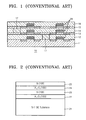
- FIG. 1 is a cross-sectional view of a conventional three-dimensional semiconductor device 10 .
- the three-dimensional semiconductor device 10 may have a structure in which insulating layers 12 , 14 , and 16 and silicon film layers 13 and 15 may be alternately stacked on a silicon substrate 11 .
- a plurality of thin film transistors TR e.g., CMOS transistors, transistors associated with memory storage, etc.
- the silicon layers 11 , 13 , and 15 may be electrically connected to each other through conductive plugs 17 .
- the three-dimensional semiconductor device 10 may be manufactured by stacking the silicon film layers 13 and 15 on the insulating layers 12 and 14 may thereby be configured to have higher charge mobility. Accordingly, the silicon film layers 13 and 15 may be manufactured to be highly oriented silicon films (e.g., approximating single crystals). However, conventional processes may not be capable of epitaxially growing highly oriented silicon film on an insulating layer.
- the silicon film may be recrystallized to approximate a single crystal silicon via a laser annealing process performed after forming amorphous silicon or polycrystalline silicon on the insulating layers 12 and 14 , growing the silicon film toward lateral directions from the conductive plugs 17 , or alternatively bonding an individually grown single crystal silicon film to the insulating layers 12 and 14 .
- each of the above-described conventional processes for attempting to approximate single crystal-type silicon films may be performed relatively high temperatures, may consume a relatively long period of time to perform and thereby may be associated with higher manufacturing or fabrication costs.
- a resultant orientation may not be controlled precisely, and grain boundaries may be generated in a resultant product.
- FIG. 2 is a cross-sectional view illustrating a conventional structure used to form a highly oriented silicon film.
- FIG. 2 illustrates a structure including a growing silicon layer oriented in a ⁇ 100> direction (e.g., a direction coinciding with a miller index direction of ⁇ 100> with respect to a crystallographic plane) on a ⁇ (gamma)-Al 2 O 3 layer. If an Al 2 O 3 layer 22 is formed on a silicon substrate 21 oriented in the ⁇ 100> direction, the Al 2 O 3 layer 22 may become a ⁇ -Al 2 O 3 oriented in the ⁇ 100> direction.
- the silicon layer 23 may be oriented in the ⁇ 100> direction.
- the ⁇ -Al 2 O 3 layers 22 and 24 and (100)-silicon layers 23 and 25 may be repeatedly stacked.
- the “stacking” of layers in the structure of FIG. 2 may be facilitated by the lattice mismatch between a ⁇ -Al 2 O 3 crystal and a (100)-silicon crystal, which may typically be maintained between 2.4 to 3.5%.
- the above-described conventional process may have difficulty controlling an orientation of the silicon substrate 21 .
- the conventional stacking structure shown in FIG. 2 may employed to fabricate a semiconductor device.
- the Al 2 O 3 layer 22 may only be highly oriented if formed on another highly oriented layer (e.g., a silicon layer).
- another highly oriented layer e.g., a silicon layer.
- the resultant Al 2 O 3 layer 22 may not be highly oriented. Accordingly, the conventional stacking structure of FIG. 2 may typically not be deployed during a fabrication of semiconductor devices.
- An example embodiment of the present invention is directed to a method of forming a semiconductor device, including forming a first layer on a substrates, the first layer including aluminum nitride (AlN), forming a second layer by oxidizing a surface of the first layer and forming a third layer on the second layer, the first, second and third layers each being highly oriented with respect to one of a plurality crystallographic planes.
- AlN aluminum nitride
- Another example embodiment of the present invention is directed to a semiconductor device, including a substrate including a first layer, the first layer including aluminum nitride (AlN), a second layer formed by oxidizing a surface of the first layer and a third layer formed on the second layer, the first, second and third layers each being highly oriented with respect to one of a plurality crystallographic planes.
- AlN aluminum nitride
- Another example embodiment of the present invention is directed to a method of forming a highly oriented silicon film, including forming an aluminum nitride (AlN) layer on a substrate, oxidizing a surface of the AlN layer to form an Al2O3 layer, the Al2O3 layer being highly oriented with respect to one of a plurality of crystallographic planes and growing a highly oriented silicon layer on the Al2O3 layer.
- AlN aluminum nitride
- example embodiments of the present invention are directed to a method of forming a highly oriented silicon film.
- the method may be performed at lower temperatures, and may be compatible with conventional semiconductor manufacturing processes, such that an orientation of the silicon film may be more effectively controlled.
- FIG. 1 Another example embodiments of the present invention are directed to a method of manufacturing a three-dimensional semiconductor device using the highly oriented silicon film, and the three-dimensional semiconductor device manufactured using the above method.
- FIG. 1 is a cross-sectional view of a conventional three-dimensional semiconductor device.
- FIG. 2 is a cross-sectional view illustrating a conventional structure used to form a highly oriented silicon film.
- FIGS. 3A through 3C are cross-sectional views illustrating a process of forming a highly oriented silicon film according to an example embodiment of the present invention.
- FIG. 4 is a graph illustrating results of X-ray diffraction (XRD) performed on an AlN film according to another example embodiment of the present invention.
- FIG. 5 is a cross-sectional view illustrating a stacking structure of a plurality of highly oriented silicon films according to another example embodiment of the present invention.
- the term “highly oriented” describes the nature of the referenced layer and includes both layers having relatively small degree of divergence from a given crystallographic plane and layers in which substantially all of the material exhibits the same crystallographic structure.
- the different layers may vary, in orientation, by a few degrees in their respective miller index orientations or may include some minor regions exhibiting a different crystallographic structure.
- the descriptive term “highly oriented” is thereby intended as a relative measure of a layer's adherence to a given crystallographic plane and/or the uniformity of the crystallographic orientation within the referenced film.
- FIGS. 3A through 3C are cross-sectional views illustrating a process of forming a highly oriented silicon film according to an example embodiment of the present invention.
- a SiO 2 layer 32 (e.g., an insulating layer) may be formed on a silicon substrate 31 , and a highly oriented AlN film 33 , oriented in a given direction, may be formed on the SiO 2 layer 32 . Because the AlN film 33 may be formed on the SiO 2 layer 32 , it will be appreciated that the SiO 2 layer 32 may function as a substrate (e.g., such as substrate 21 in conventional FIG. 1 ). While the insulating layer 32 is above described and illustrated as including SiO 2 , it will be appreciated that any well-known insulation material may alternatively be used.
- the insulating layer 32 may include one or more of Si 3 N 4 and Al 2 O 3 in place of or in addition to SiO 2 , in other example embodiments of the present invention.
- the AlN film 33 may be formed by any of a number of processes, including but not limited to a sputtering process, a metalorganic chemical vapor deposition (MOCVD) process, a physical vapor deposition (PVD) process and/or a chemical vapor, deposition (CVD) process.
- the AlN film 33 may be formed on the insulating layer 32 , which as described above, may include materials such as SiO 2 , Si 3 N 4 and/or Al 2 O 3 , such that the AlN film 33 may be substantially uniformly oriented in a direction substantially perpendicular to an upper surface of the substrate 31 , or a c-axis.
- FIG. 4 is a graph illustrating results of X-ray diffraction (XRD) performed on the AlN film 33 according to another example embodiment of the present invention.
- the AlN film 33 may be formed at room temperature using a sputtering method by supplying nitrogen and argon gases at flow rates of 39 sccm and 6 sccm, respectively, with a power supply of approximately 7000 W AC.
- peaks in ⁇ 002> and ⁇ 004> directions are shown because the AlN film 33 may be c-axis oriented.
- a relatively large peak may be shown in the ⁇ 002> direction, which may be indicative of an orientation of the AlN film 33 being substantially oriented in the ⁇ 002> direction.
- the thickness for the AlN film 33 there is no particular limitation of the thickness for the AlN film 33 .
- the AlN film 33 may be maintained to be a relatively thin layer so as to reduce a size of a three-dimensional semiconductor device.
- a factor which may contribute to a desired thickness of the AlN film 33 may be a correlation between thickness and orientation uniformity, wherein the orientation of the AlN film 33 may become more uniform as a thickness thereof increases.
- the thickness of the AlN film 33 may be selected based upon uniformity characteristics as well as size limitations.
- the AlN film 33 may have a thickness between about 30 to about 500 nm.
- a highly oriented ⁇ -Al 2 O 3 layer or ⁇ -Al 2 O 3 layer 34 may be formed on a surface of the AlN film 33 by oxidizing the highly oriented AlN film 33 .
- the highly oriented ⁇ -Al 2 O 3 layer or ⁇ -Al 2 O 3 layer 34 may be formed by thermally oxidizing the highly oriented AlN film 33 at a temperature between about 500 to about 1000° C. in an oxygen or ozone gas atmosphere. In this process, nitrogen may be reduced or removed from the surface of the AlN film 33 , and Al 2 O 3 may be formed by combining oxygen with aluminum.
- a ⁇ -Al 2 O 3 layer or, an ⁇ -Al 2 O 3 layer or a mixed layer comprised of ⁇ -Al 2 O 3 and ⁇ -Al 2 O 3 may be formed.
- any of the Al 2 O 3 layers formed in the above-described manner may be crystals having a shorter-range order, and may be oriented in the c-axis direction so as to be substantially perpendicular to an upper surface of the substrate 31 similar to the AlN film 33 .
- one or more of the Al 2 O 3 may be ⁇ -Al 2 O 3 and/or ⁇ -Al 2 O 3 may be oriented in the ⁇ 001>direction.
- a surface of the highly oriented ⁇ -Al 2 O 3 layer and/or ⁇ -Al 2 O 3 layer 34 may be washed using, for example, a diluted hydrogen fluoride (HF) solution to reduce or remove, remaining impurities from the surface. not be highly oriented. Accordingly, the conventional stacking structure of FIG. 2 may typically not be deployed during a fabrication of semiconductor devices.
- HF diluted hydrogen fluoride
- An example embodiment of the present invention is directed to a method of forming a semiconductor device, including forming a first layer on a substrate, the first layer including aluminum nitride (AlN), forming a second layer by oxidizing a surface of the first layer and forming a third layer on the second layer, the first, second and third layers each being highly oriented with respect to one of a plurality crystallographic planes.
- AlN aluminum nitride
- Another example embodiment of the present invention is directed to a semiconductor device, including a substrate including a first layer, the first layer including aluminum nitride (AlN), a second layer formed by oxidizing a surface of the first layer and a third layer formed on the second layer, the first, second and third layers each being highly oriented with respect to one of a plurality crystallographic planes.
- AlN aluminum nitride
- Another example embodiment of the present invention is directed to a method of forming a highly oriented silicon film, including forming an aluminum nitride (AlN) layer on a substrate, oxidizing a surface of the AlN layer to form an Al2O3 layer, the Al2O3 layer being highly oriented with respect to one of a plurality of crystallographic planes and growing a highly oriented silicon layer on the Al2O3 layer.
- AlN aluminum nitride
- example embodiments of the present invention are directed to a method of forming a highly oriented silicon film.
- the method may be performed at lower temperatures, and may be compatible with conventional semiconductor manufacturing processes, such that an orientation of the silicon film may be more effectively controlled.
- FIG. 1 Another example embodiments of the present invention are directed to a method of manufacturing a three-dimensional semiconductor device using the highly oriented silicon film, and the three-dimensional semiconductor device manufactured using the above method.
- a second multilayer 120 may include a SiO 2 layer 121 , a highly oriented AlN film 122 , a highly oriented ⁇ -Al 2 O 3 layer 123 and a highly oriented silicon film 124 .
- the second multilayer 120 may be formed on the highly oriented silicon film 114 .
- additional multilayers may be stacked on the silicon film 124 in a manner similar to that of the second multilayer 120 on the first multilayer 110 .
- a three-dimensional semiconductor device may be manufactured by forming thin film transistors, such as CMOS devices or electronic devices such as memory devices, on upper surfaces of the silicon substrate 100 and the highly oriented silicon films 114 and 124 as shown in the example embodiment of FIG. 5 .
- an electronic device such as a thin film transistor or a memory, may be formed on the silicon substrate 100 by forming a gate insulating layer (not shown) and a gate electrode (not shown) between two doped regions, which may be formed by doping an n-dopant and a p-dopant on given regions of the silicon substrate 100 (e.g., with any well-known doping process).
- the SiO 2 layer 111 , the highly oriented AlN film 112 , the highly oriented ⁇ -Al 2 O 3 layer 113 and the highly oriented silicon film 114 may be sequentially formed on the silicon substrate 100 .
- an electronic device such as a thin film transistor or a memory, may be formed on an upper surface of the highly oriented silicon film 114 using the above process, which may thereby form the three-dimensional semiconductor device (e.g., if performed repeatedly).
- a highly oriented silicon film may be formed on an insulating layer by forming a buffer layer including AlN.
- the highly oriented silicon film according to the present invention may be manufactured using a lower temperature process and also employing a process which may be compatible with conventional manufacturing processes. Accordingly, manufacture of a three-dimensional semiconductor device according to example embodiments of the present invention may be associated with lower costs and a simpler process (e.g., because lower temperatures may be used) as compared to conventional fabrication processes.
- a highly oriented silicon film may be formed by forming a buffer layer including aluminum nitride (AlN) on an insulating layer.
- AlN aluminum nitride
- Example embodiments of the present invention being thus described, it will be obvious that the same may be varied in many ways.
- example embodiments are above described as being related to epitaxial growing silicon film, it is understood that other example embodiments of the present invention need not be limited to a “silicon” film.
- other example embodiments of the present invention may deploy one or more semiconductor films, in place of or in addition to the silicon film, such as GaN, Fe 3 O 4 , etc.
- compositions of the particular layers have been above-described and illustrated as including particular compositions.
- the substrate 31 is above described as including silicon, whereas other example embodiments may include any well-known substrates, and need not be limited to “silicon” substrates.
- the ⁇ -Al 2 O 3 layer or ⁇ -Al 2 O 3 layer 34 and the SiO 2 layer 32 may each be configured to include other materials in addition to or in place of the particular compositions given above for example purposes.
Landscapes
- Recrystallisation Techniques (AREA)
- Formation Of Insulating Films (AREA)
- Non-Volatile Memory (AREA)
- Insulated Gate Type Field-Effect Transistor (AREA)
- Thin Film Transistor (AREA)
- Semiconductor Memories (AREA)
Abstract
Description
Claims (25)
Applications Claiming Priority (2)
| Application Number | Priority Date | Filing Date | Title |
|---|---|---|---|
| KR10-2006-0037219 | 2006-04-25 | ||
| KR1020060037219A KR100707215B1 (en) | 2006-04-25 | 2006-04-25 | Highly Oriented Silicon Thin Film Formation Method, 3D Semiconductor Device Manufacturing Method and 3D Semiconductor Device |
Publications (2)
| Publication Number | Publication Date |
|---|---|
| US20070246802A1 US20070246802A1 (en) | 2007-10-25 |
| US8097499B2 true US8097499B2 (en) | 2012-01-17 |
Family
ID=37772798
Family Applications (1)
| Application Number | Title | Priority Date | Filing Date |
|---|---|---|---|
| US11/702,624 Expired - Fee Related US8097499B2 (en) | 2006-04-25 | 2007-02-06 | Semiconductor device and methods thereof |
Country Status (5)
| Country | Link |
|---|---|
| US (1) | US8097499B2 (en) |
| EP (1) | EP1850373B1 (en) |
| JP (1) | JP5230116B2 (en) |
| KR (1) | KR100707215B1 (en) |
| CN (1) | CN101064258B (en) |
Families Citing this family (10)
| Publication number | Priority date | Publication date | Assignee | Title |
|---|---|---|---|---|
| EP2071053B1 (en) * | 2006-09-29 | 2019-02-27 | Toyoda Gosei Co., Ltd. | Filming method for iii-group nitride semiconductor laminated structure |
| US20110030773A1 (en) * | 2009-08-06 | 2011-02-10 | Alliance For Sustainable Energy, Llc | Photovoltaic cell with back-surface reflectivity scattering |
| US8466447B2 (en) | 2009-08-06 | 2013-06-18 | Alliance For Sustainable Energy, Llc | Back contact to film silicon on metal for photovoltaic cells |
| US20110244663A1 (en) * | 2010-04-01 | 2011-10-06 | Applied Materials, Inc. | Forming a compound-nitride structure that includes a nucleation layer |
| WO2013145404A1 (en) * | 2012-03-28 | 2013-10-03 | 株式会社豊田中央研究所 | Laminated substate of silicon single crystal and group iii nitride single crystal with off angle |
| JP5491679B1 (en) * | 2012-06-29 | 2014-05-14 | パナソニック株式会社 | Nitride semiconductor light emitting device |
| CN103014622A (en) * | 2012-12-11 | 2013-04-03 | 常州大学 | Method for preparing high-oriented AlN thin film |
| US9929310B2 (en) | 2013-03-14 | 2018-03-27 | Applied Materials, Inc. | Oxygen controlled PVD aluminum nitride buffer for gallium nitride-based optoelectronic and electronic devices |
| CN105977136A (en) * | 2016-05-27 | 2016-09-28 | 清华大学 | Semiconductor structure and method for preparing the same |
| JP2023134876A (en) * | 2022-03-15 | 2023-09-28 | キオクシア株式会社 | Oxide film manufacturing method, semiconductor storage device manufacturing method, semiconductor device, and semiconductor storage device |
Citations (6)
| Publication number | Priority date | Publication date | Assignee | Title |
|---|---|---|---|---|
| US4511816A (en) * | 1982-03-11 | 1985-04-16 | Nobuo Mikoshiba | Surface acoustic wave device using an elastic substrate and an aluminum nitride piezoelectric film |
| US5583369A (en) * | 1992-07-06 | 1996-12-10 | Semiconductor Energy Laboratory Co., Ltd. | Semiconductor device and method for forming the same |
| US20020037599A1 (en) * | 2000-08-08 | 2002-03-28 | Masahiro Ishida | Semiconductor substrate, method of manufacturing the semiconductor substrate, semiconductor device and pattern forming method |
| US20030210722A1 (en) * | 2002-03-11 | 2003-11-13 | Takahiro Arakida | Semiconductor laser device |
| JP2004051446A (en) * | 2002-07-22 | 2004-02-19 | Asahi Kasei Corp | Method for forming oxide single crystal thin film and method for forming semiconductor thin film |
| US20060292313A1 (en) * | 2005-06-24 | 2006-12-28 | Wenxu Xianyu | Methods of forming a more highly-oriented silicon layer and substrate having the same |
Family Cites Families (10)
| Publication number | Priority date | Publication date | Assignee | Title |
|---|---|---|---|---|
| JP2721258B2 (en) * | 1990-02-05 | 1998-03-04 | 日立金属株式会社 | Manufacturing method of ceramic substrate |
| JPH0480945A (en) * | 1990-07-24 | 1992-03-13 | Toshiba Corp | Manufacture of semiconductor device |
| JP2828152B2 (en) * | 1991-08-13 | 1998-11-25 | 富士通 株式会社 | Method of forming thin film, multilayer structure film, and method of forming silicon thin film transistor |
| JPH082998A (en) * | 1994-06-15 | 1996-01-09 | Sumitomo Electric Ind Ltd | Oxide dielectric thin film and manufacturing method thereof |
| JP3688802B2 (en) * | 1996-04-30 | 2005-08-31 | 誠 石田 | Method for manufacturing SOI structure |
| JPH11233440A (en) * | 1998-02-13 | 1999-08-27 | Toshiba Corp | Semiconductor device |
| WO2001004943A1 (en) * | 1999-07-07 | 2001-01-18 | Matsushita Electric Industrial Co., Ltd. | Multilayered body, method for fabricating multilayered body, and semiconductor device |
| JP2001196896A (en) | 2000-01-11 | 2001-07-19 | Seiko Epson Corp | Surface acoustic wave device |
| JP3867161B2 (en) * | 2002-09-20 | 2007-01-10 | 独立行政法人物質・材料研究機構 | Thin film element |
| JP2004152814A (en) * | 2002-10-29 | 2004-05-27 | Toyota Motor Corp | Semiconductor element substrate and method of manufacturing the same |
-
2006
- 2006-04-25 KR KR1020060037219A patent/KR100707215B1/en not_active Expired - Fee Related
- 2006-08-30 CN CN200610126325XA patent/CN101064258B/en not_active Expired - Fee Related
- 2006-11-20 EP EP06124375.4A patent/EP1850373B1/en not_active Ceased
-
2007
- 2007-02-06 US US11/702,624 patent/US8097499B2/en not_active Expired - Fee Related
- 2007-03-15 JP JP2007067186A patent/JP5230116B2/en active Active
Patent Citations (7)
| Publication number | Priority date | Publication date | Assignee | Title |
|---|---|---|---|---|
| US4511816A (en) * | 1982-03-11 | 1985-04-16 | Nobuo Mikoshiba | Surface acoustic wave device using an elastic substrate and an aluminum nitride piezoelectric film |
| US5583369A (en) * | 1992-07-06 | 1996-12-10 | Semiconductor Energy Laboratory Co., Ltd. | Semiconductor device and method for forming the same |
| US20020037599A1 (en) * | 2000-08-08 | 2002-03-28 | Masahiro Ishida | Semiconductor substrate, method of manufacturing the semiconductor substrate, semiconductor device and pattern forming method |
| US20030210722A1 (en) * | 2002-03-11 | 2003-11-13 | Takahiro Arakida | Semiconductor laser device |
| JP2004051446A (en) * | 2002-07-22 | 2004-02-19 | Asahi Kasei Corp | Method for forming oxide single crystal thin film and method for forming semiconductor thin film |
| US20060292313A1 (en) * | 2005-06-24 | 2006-12-28 | Wenxu Xianyu | Methods of forming a more highly-oriented silicon layer and substrate having the same |
| US7662678B2 (en) * | 2005-06-24 | 2010-02-16 | Samsung Electronics Co., Ltd. | Method of forming a more highly-oriented silicon layer and substrate having the same |
Non-Patent Citations (10)
| Title |
|---|
| Brunet et al., "Highly textured hexagonal AlN films deposited at low temperature by reactive cathodic sputtering", Materials Science and Engineering, vol. B59, pp. 88-93 (1999). |
| European Search Report dated Dec. 29, 2010 in corresponding European Application No. 06124375.4. |
| European Search Report dated Jan. 5, 2010 in corresponding European Application No. 06124375.4. |
| Ishida et al., "Double SOI Structures and Devices Applications with Heteroepitaxial Al2O3 and Si" Jpn. J. Appl. Phys., vol. 34 (1995), pp. 831-835, Part 1, No. 2B. |
| Ishida et al., "Epitaxially Stacked Structures of Si/ A12O3/Si for Sensor Materials," Sensors and Actuators, A21-A23, (1990) 267-270. |
| Kang et al., "Synthesis of epitaxial gamma-A12O3 thin films by thermal oxidation of AlN/sapphire(0001) thin films", Appl. Phys., vol. A77, pp. 627-632 (2003). |
| Kang et al., "Synthesis of epitaxial γ-A12O3 thin films by thermal oxidation of AlN/sapphire(0001) thin films", Appl. Phys., vol. A77, pp. 627-632 (2003). |
| Kemmer et al., "Epitaxy-a new technology for fabrication of advanced silicon radiation detectors", 2005, Nuclear Instruments and Methods in Physics Research A, 544, pp. 612-619. * |
| Lin et al., "Epitaxial growth of cubic AlN films on (100) and (111) silicon by pulsed laser ablation", Appl. Phys. Lett., vol. 66, No. 16, pp. 2066-2068 (Apr. 17, 1995). |
| Wittkower, "Smart-Cut Technology for SOI: A new high volume application for ion implantation", 2000, IEEE pp. 269-272. * |
Also Published As
| Publication number | Publication date |
|---|---|
| EP1850373A3 (en) | 2010-02-03 |
| CN101064258A (en) | 2007-10-31 |
| CN101064258B (en) | 2012-04-25 |
| EP1850373A2 (en) | 2007-10-31 |
| EP1850373B1 (en) | 2017-06-14 |
| KR100707215B1 (en) | 2007-04-13 |
| JP5230116B2 (en) | 2013-07-10 |
| JP2007294898A (en) | 2007-11-08 |
| US20070246802A1 (en) | 2007-10-25 |
Similar Documents
| Publication | Publication Date | Title |
|---|---|---|
| US8097499B2 (en) | Semiconductor device and methods thereof | |
| CN105579613B (en) | Method and apparatus for forming device-quality gallium nitride layers on silicon substrates | |
| US11615955B2 (en) | Material having single crystal perovskite, device including the same, and manufacturing method thereof | |
| TWI501291B (en) | Method for forming epitaxial wafers and method for fabricating semiconductor elements | |
| CN104051232B (en) | Semiconductor wafer with a layerof alzga1-zn and process for producing it | |
| US9105471B2 (en) | Rare earth oxy-nitride buffered III-N on silicon | |
| CN102714162A (en) | Group III Nitride Epitaxial Laminated Substrates | |
| US9437688B2 (en) | High-quality GaN high-voltage HFETs on silicon | |
| JP2016515299A (en) | III-N semiconductor device grown on a silicon substrate with a rare earth oxide gate dielectric | |
| US8685828B2 (en) | Method of forming a capacitor | |
| KR20090106112A (en) | Deposition of Aluminum Nitride Films for Micro or Nanoelectromechanical Systems on Polycrystalline Silicon Carbide Buffer Layers | |
| JP5997258B2 (en) | Stacked substrate of silicon single crystal and group III nitride single crystal having off-angle, and method for manufacturing the same | |
| TW201135886A (en) | Semiconductor substrate, electronic device and method for manufacturing semiconductor substrate | |
| JP2004296701A (en) | Epitaxial substrate, semiconductor device, and crystal growth method for nitride semiconductor | |
| JP7533794B2 (en) | Method for manufacturing nitride semiconductor substrate | |
| CN117568936A (en) | An AlN-ScN superlattice material and its preparation method | |
| US9231053B2 (en) | Light emitting diodes having zinc oxide fibers over silicon substrates | |
| WO2016132746A1 (en) | THIN-FILM SUBSTRATE, SEMICONDUCTOR DEVICE AND MANUFACTURING METHOD THEREFOR, DEPOSITION APPARATUS, DEPOSITION METHOD AND GaN TEMPLATE | |
| JP2020070196A (en) | Nitride semiconductor layer growth method | |
| JP4208078B2 (en) | InN semiconductor and manufacturing method thereof |
Legal Events
| Date | Code | Title | Description |
|---|---|---|---|
| AS | Assignment |
Owner name: SAMSUNG ELECTRONICS CO., LTD., KOREA, REPUBLIC OF Free format text: ASSIGNMENT OF ASSIGNORS INTEREST;ASSIGNORS:XIANYU, WENXU;PARK, YOUNG-SOO;LEE, JUN-HO;AND OTHERS;REEL/FRAME:018979/0445 Effective date: 20061129 |
|
| ZAAA | Notice of allowance and fees due |
Free format text: ORIGINAL CODE: NOA |
|
| ZAAB | Notice of allowance mailed |
Free format text: ORIGINAL CODE: MN/=. |
|
| FEPP | Fee payment procedure |
Free format text: PAYOR NUMBER ASSIGNED (ORIGINAL EVENT CODE: ASPN); ENTITY STATUS OF PATENT OWNER: LARGE ENTITY |
|
| STCF | Information on status: patent grant |
Free format text: PATENTED CASE |
|
| FPAY | Fee payment |
Year of fee payment: 4 |
|
| MAFP | Maintenance fee payment |
Free format text: PAYMENT OF MAINTENANCE FEE, 8TH YEAR, LARGE ENTITY (ORIGINAL EVENT CODE: M1552); ENTITY STATUS OF PATENT OWNER: LARGE ENTITY Year of fee payment: 8 |
|
| FEPP | Fee payment procedure |
Free format text: MAINTENANCE FEE REMINDER MAILED (ORIGINAL EVENT CODE: REM.); ENTITY STATUS OF PATENT OWNER: LARGE ENTITY |
|
| LAPS | Lapse for failure to pay maintenance fees |
Free format text: PATENT EXPIRED FOR FAILURE TO PAY MAINTENANCE FEES (ORIGINAL EVENT CODE: EXP.); ENTITY STATUS OF PATENT OWNER: LARGE ENTITY |
|
| STCH | Information on status: patent discontinuation |
Free format text: PATENT EXPIRED DUE TO NONPAYMENT OF MAINTENANCE FEES UNDER 37 CFR 1.362 |
|
| FP | Lapsed due to failure to pay maintenance fee |
Effective date: 20240117 |