US8097344B2 - Electronic device housing - Google Patents
Electronic device housing Download PDFInfo
- Publication number
- US8097344B2 US8097344B2 US12/949,942 US94994210A US8097344B2 US 8097344 B2 US8097344 B2 US 8097344B2 US 94994210 A US94994210 A US 94994210A US 8097344 B2 US8097344 B2 US 8097344B2
- Authority
- US
- United States
- Prior art keywords
- coating
- electronic device
- device housing
- titanium dioxide
- metallic
- Prior art date
- Legal status (The legal status is an assumption and is not a legal conclusion. Google has not performed a legal analysis and makes no representation as to the accuracy of the status listed.)
- Expired - Fee Related
Links
Images

Classifications
-
- H—ELECTRICITY
- H05—ELECTRIC TECHNIQUES NOT OTHERWISE PROVIDED FOR
- H05K—PRINTED CIRCUITS; CASINGS OR CONSTRUCTIONAL DETAILS OF ELECTRIC APPARATUS; MANUFACTURE OF ASSEMBLAGES OF ELECTRICAL COMPONENTS
- H05K5/00—Casings, cabinets or drawers for electric apparatus
- H05K5/02—Details
- H05K5/0217—Mechanical details of casings
- H05K5/0243—Mechanical details of casings for decorative purposes
-
- C—CHEMISTRY; METALLURGY
- C09—DYES; PAINTS; POLISHES; NATURAL RESINS; ADHESIVES; COMPOSITIONS NOT OTHERWISE PROVIDED FOR; APPLICATIONS OF MATERIALS NOT OTHERWISE PROVIDED FOR
- C09D—COATING COMPOSITIONS, e.g. PAINTS, VARNISHES OR LACQUERS; FILLING PASTES; CHEMICAL PAINT OR INK REMOVERS; INKS; CORRECTING FLUIDS; WOODSTAINS; PASTES OR SOLIDS FOR COLOURING OR PRINTING; USE OF MATERIALS THEREFOR
- C09D1/00—Coating compositions, e.g. paints, varnishes or lacquers, based on inorganic substances
-
- C—CHEMISTRY; METALLURGY
- C09—DYES; PAINTS; POLISHES; NATURAL RESINS; ADHESIVES; COMPOSITIONS NOT OTHERWISE PROVIDED FOR; APPLICATIONS OF MATERIALS NOT OTHERWISE PROVIDED FOR
- C09D—COATING COMPOSITIONS, e.g. PAINTS, VARNISHES OR LACQUERS; FILLING PASTES; CHEMICAL PAINT OR INK REMOVERS; INKS; CORRECTING FLUIDS; WOODSTAINS; PASTES OR SOLIDS FOR COLOURING OR PRINTING; USE OF MATERIALS THEREFOR
- C09D161/00—Coating compositions based on condensation polymers of aldehydes or ketones; Coating compositions based on derivatives of such polymers
- C09D161/04—Condensation polymers of aldehydes or ketones with phenols only
-
- C—CHEMISTRY; METALLURGY
- C09—DYES; PAINTS; POLISHES; NATURAL RESINS; ADHESIVES; COMPOSITIONS NOT OTHERWISE PROVIDED FOR; APPLICATIONS OF MATERIALS NOT OTHERWISE PROVIDED FOR
- C09D—COATING COMPOSITIONS, e.g. PAINTS, VARNISHES OR LACQUERS; FILLING PASTES; CHEMICAL PAINT OR INK REMOVERS; INKS; CORRECTING FLUIDS; WOODSTAINS; PASTES OR SOLIDS FOR COLOURING OR PRINTING; USE OF MATERIALS THEREFOR
- C09D175/00—Coating compositions based on polyureas or polyurethanes; Coating compositions based on derivatives of such polymers
- C09D175/04—Polyurethanes
-
- C—CHEMISTRY; METALLURGY
- C09—DYES; PAINTS; POLISHES; NATURAL RESINS; ADHESIVES; COMPOSITIONS NOT OTHERWISE PROVIDED FOR; APPLICATIONS OF MATERIALS NOT OTHERWISE PROVIDED FOR
- C09D—COATING COMPOSITIONS, e.g. PAINTS, VARNISHES OR LACQUERS; FILLING PASTES; CHEMICAL PAINT OR INK REMOVERS; INKS; CORRECTING FLUIDS; WOODSTAINS; PASTES OR SOLIDS FOR COLOURING OR PRINTING; USE OF MATERIALS THEREFOR
- C09D5/00—Coating compositions, e.g. paints, varnishes or lacquers, characterised by their physical nature or the effects produced; Filling pastes
- C09D5/16—Antifouling paints; Underwater paints
- C09D5/1606—Antifouling paints; Underwater paints characterised by the anti-fouling agent
- C09D5/1612—Non-macromolecular compounds
- C09D5/1618—Non-macromolecular compounds inorganic
-
- C—CHEMISTRY; METALLURGY
- C09—DYES; PAINTS; POLISHES; NATURAL RESINS; ADHESIVES; COMPOSITIONS NOT OTHERWISE PROVIDED FOR; APPLICATIONS OF MATERIALS NOT OTHERWISE PROVIDED FOR
- C09D—COATING COMPOSITIONS, e.g. PAINTS, VARNISHES OR LACQUERS; FILLING PASTES; CHEMICAL PAINT OR INK REMOVERS; INKS; CORRECTING FLUIDS; WOODSTAINS; PASTES OR SOLIDS FOR COLOURING OR PRINTING; USE OF MATERIALS THEREFOR
- C09D7/00—Features of coating compositions, not provided for in group C09D5/00; Processes for incorporating ingredients in coating compositions
- C09D7/40—Additives
- C09D7/60—Additives non-macromolecular
- C09D7/61—Additives non-macromolecular inorganic
-
- C—CHEMISTRY; METALLURGY
- C09—DYES; PAINTS; POLISHES; NATURAL RESINS; ADHESIVES; COMPOSITIONS NOT OTHERWISE PROVIDED FOR; APPLICATIONS OF MATERIALS NOT OTHERWISE PROVIDED FOR
- C09D—COATING COMPOSITIONS, e.g. PAINTS, VARNISHES OR LACQUERS; FILLING PASTES; CHEMICAL PAINT OR INK REMOVERS; INKS; CORRECTING FLUIDS; WOODSTAINS; PASTES OR SOLIDS FOR COLOURING OR PRINTING; USE OF MATERIALS THEREFOR
- C09D7/00—Features of coating compositions, not provided for in group C09D5/00; Processes for incorporating ingredients in coating compositions
- C09D7/40—Additives
- C09D7/66—Additives characterised by particle size
- C09D7/67—Particle size smaller than 100 nm
-
- C—CHEMISTRY; METALLURGY
- C08—ORGANIC MACROMOLECULAR COMPOUNDS; THEIR PREPARATION OR CHEMICAL WORKING-UP; COMPOSITIONS BASED THEREON
- C08K—Use of inorganic or non-macromolecular organic substances as compounding ingredients
- C08K2201/00—Specific properties of additives
- C08K2201/011—Nanostructured additives
-
- C—CHEMISTRY; METALLURGY
- C08—ORGANIC MACROMOLECULAR COMPOUNDS; THEIR PREPARATION OR CHEMICAL WORKING-UP; COMPOSITIONS BASED THEREON
- C08K—Use of inorganic or non-macromolecular organic substances as compounding ingredients
- C08K3/00—Use of inorganic substances as compounding ingredients
- C08K3/18—Oxygen-containing compounds, e.g. metal carbonyls
- C08K3/20—Oxides; Hydroxides
- C08K3/22—Oxides; Hydroxides of metals
-
- C—CHEMISTRY; METALLURGY
- C08—ORGANIC MACROMOLECULAR COMPOUNDS; THEIR PREPARATION OR CHEMICAL WORKING-UP; COMPOSITIONS BASED THEREON
- C08K—Use of inorganic or non-macromolecular organic substances as compounding ingredients
- C08K3/00—Use of inorganic substances as compounding ingredients
- C08K3/34—Silicon-containing compounds
- C08K3/36—Silica
-
- H—ELECTRICITY
- H04—ELECTRIC COMMUNICATION TECHNIQUE
- H04M—TELEPHONIC COMMUNICATION
- H04M1/00—Substation equipment, e.g. for use by subscribers
- H04M1/02—Constructional features of telephone sets
- H04M1/0202—Portable telephone sets, e.g. cordless phones, mobile phones or bar type handsets
- H04M1/0279—Improving the user comfort or ergonomics
- H04M1/0283—Improving the user comfort or ergonomics for providing a decorative aspect, e.g. customization of casings, exchangeable faceplate
-
- Y—GENERAL TAGGING OF NEW TECHNOLOGICAL DEVELOPMENTS; GENERAL TAGGING OF CROSS-SECTIONAL TECHNOLOGIES SPANNING OVER SEVERAL SECTIONS OF THE IPC; TECHNICAL SUBJECTS COVERED BY FORMER USPC CROSS-REFERENCE ART COLLECTIONS [XRACs] AND DIGESTS
- Y10—TECHNICAL SUBJECTS COVERED BY FORMER USPC
- Y10T—TECHNICAL SUBJECTS COVERED BY FORMER US CLASSIFICATION
- Y10T428/00—Stock material or miscellaneous articles
- Y10T428/25—Web or sheet containing structurally defined element or component and including a second component containing structurally defined particles
- Y10T428/256—Heavy metal or aluminum or compound thereof
- Y10T428/257—Iron oxide or aluminum oxide
Definitions
- the present disclosure relates to electronic device housings, particularly to an electronic device housing having a self-cleaning property.
- Decorative metallic coatings are often formed on housings of electronic devices.
- the metallic coatings are typically formed by vacuum deposition for an aesthetic metallic appearance.
- the metallic coatings formed by vacuum deposition can be nonconductive so as not to block electromagnetic waves.
- the metallic coatings are not self-cleaning, and cannot repel dust and sweat that collects on the electronic device housings.
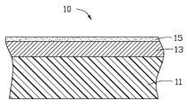
- FIGURE Many aspects of the electronic device housing can be better understood with reference to the following FIGURE.
- the components in the FIGURE are not necessarily drawn to scale, the emphasis instead being placed upon clearly illustrating the principles of the electronic device housing.
- the FIGURE is a cross-section of an embodiment of an electronic device housing.
- the FIGURE shows an electronic device housing 10 according to an embodiment.
- the electronic device housing 10 includes a substrate 11 , a metallic coating 13 formed on a surface of the substrate 11 , and a top paint coating 15 formed on the metallic coating 13 .
- the electronic device housing 10 may be a housing of a mobile phone, PDA, note book computer, MP3, MP4, GPS navigator, or digital camera.
- the substrate 11 may be formed by molding one or more plastics such as polycarbonate (PC), polyethylene (PE), polymethyl methacrylate (PMMA), and a mixture of polycarbonate and acrylonitrile-butadiene-styrene plastics (PC+ABS).
- PC polycarbonate
- PE polyethylene
- PMMA polymethyl methacrylate
- PC+ABS acrylonitrile-butadiene-styrene plastics
- the substrate 11 may instead be made of glass or ceramic.
- the metallic coating 13 may be a titanium dioxide coating, a composite coating formed of a titanium dioxide coating and a silicon dioxide coating, or another composite coating consisting of a titanium dioxide coating, a silicon dioxide coating, and another metallic oxide coating such as a niobium oxide coating, a zirconium oxide coating, an aluminum oxide coating, and a tantalum oxide coating. If the metallic coating 13 contains the metallic oxide coating, the exterior layer of the metallic coating 13 should be the titanium dioxide coating or the silicon dioxide coating for enhancing the bonding between the metallic coating 13 and the top paint coating 15 .
- the metallic coating 13 may be formed by vacuum sputtering or vacuum vapor deposition.
- the thickness of the metallic coating 13 may be in a range of about 10 nm to about 500 nm.
- the thickness of the metallic coating 13 is determined by how much is needed for presenting a metallic appearance without interfering with radio transmission capabilities.
- the top paint coating 15 may be formed on the metallic coating 13 by spray painting.
- the paint component for the paint coating 15 may be acrylic resin paint, epoxy resin paint, polyurethane resin paint, or phenolic resin paint.
- the paint contains nano-titanium dioxide powder and nano-silicon dioxide powder.
- the top paint coating 15 includes the nano-titanium dioxide powder and the nano-silicon dioxide powder at a mass percentage of about 5% to about 10%.
- the mass ratio of the nano-titanium dioxide powder to the nano-silicon dioxide powder may be about 3:1 to about 8:1.
- the nano-titanium dioxide powder may have an average particle size of less than 100 nm.
- the top paint coating 15 may be transparent or translucent, and has a thickness of about 10 ⁇ m to about 50 ⁇ m.
- the top paint coating 15 even if containing nano-titanium dioxide powder and nano-silicon dioxide powder, can tightly bond to the metallic coating 13 because the metallic coating 13 has an exterior layer of titanium dioxide coating or silicon dioxide coating.
- the nano-titanium dioxide powder and nano-silicon dioxide powder contained in the top paint coating 15 is directly bonded to the titanium dioxide coating or the silicon dioxide coating of the metallic coating 13 , thus enhancing the bond between the top paint coating 15 and the metallic coating 13 .
- the top paint coating 15 has a self-cleaning property. Specifically, during irradiation under visible light or ultraviolet light, the nano-titanium dioxide contained in the top paint coating 15 can oxygenize and clean off dust and sweat that have accumulated on the surface of the top paint coating 15 .
Landscapes
- Chemical & Material Sciences (AREA)
- Engineering & Computer Science (AREA)
- Life Sciences & Earth Sciences (AREA)
- Materials Engineering (AREA)
- Wood Science & Technology (AREA)
- Organic Chemistry (AREA)
- Inorganic Chemistry (AREA)
- Microelectronics & Electronic Packaging (AREA)
- Nanotechnology (AREA)
- Casings For Electric Apparatus (AREA)
- Laminated Bodies (AREA)
Abstract
Description
| Attorney | ||
| Docket No. | Title | Inventors |
| 12/949,934 | ELECTRONIC DEVICE HOUSING | QI-JIAN DU et al. |
| US 31521 | AND METHOD FOR MAKING | |
| THE SAME | ||
| US 31523 | ELECTRONIC DEVICE HOUSING | QI-JIAN DU et al. |
| 12/949,942 | ||
| US 31998 | ELECTRONIC DEVICE HOUSING | QI-JIAN DU et al. |
| 12/949,947 | ||
Claims (15)
Applications Claiming Priority (3)
| Application Number | Priority Date | Filing Date | Title |
|---|---|---|---|
| CN200910312293 | 2009-12-25 | ||
| CN2009103122936A CN102111969A (en) | 2009-12-25 | 2009-12-25 | Shell for electronic device |
| CN200910312293.6 | 2009-12-25 |
Publications (2)
| Publication Number | Publication Date |
|---|---|
| US20110159275A1 US20110159275A1 (en) | 2011-06-30 |
| US8097344B2 true US8097344B2 (en) | 2012-01-17 |
Family
ID=44175943
Family Applications (1)
| Application Number | Title | Priority Date | Filing Date |
|---|---|---|---|
| US12/949,942 Expired - Fee Related US8097344B2 (en) | 2009-12-25 | 2010-11-19 | Electronic device housing |
Country Status (2)
| Country | Link |
|---|---|
| US (1) | US8097344B2 (en) |
| CN (1) | CN102111969A (en) |
Cited By (7)
| Publication number | Priority date | Publication date | Assignee | Title |
|---|---|---|---|---|
| US20100254075A1 (en) * | 2009-04-02 | 2010-10-07 | Shenzhen Futaihong Precision Industry Co., Ltd. | Housing for electronic device |
| US20110155409A1 (en) * | 2009-12-29 | 2011-06-30 | Shenzhen Futaihong Precision Industry Co., Ltd. | Electronic device housing |
| US20110159258A1 (en) * | 2009-12-28 | 2011-06-30 | Shenzhen Futaihong Precision Industry Co., Ltd. | Electronic device housing and method for making the same |
| US20120241185A1 (en) * | 2011-03-24 | 2012-09-27 | Hon Hai Precision Industry Co., Ltd. | Electronic device housing and method of manufacturing the same |
| US20140118903A1 (en) * | 2012-11-01 | 2014-05-01 | Samsung Electronics Co. Ltd. | Case frame and manufacturing method thereof |
| US20170094825A1 (en) * | 2015-09-24 | 2017-03-30 | Cheng Uei Precision Industry Co., Ltd. | Electronics housing and manufacturing method of electronics housing |
| CN111901996A (en) * | 2020-08-05 | 2020-11-06 | Oppo广东移动通信有限公司 | Shell assembly, preparation method thereof and electronic equipment |
Families Citing this family (10)
| Publication number | Priority date | Publication date | Assignee | Title |
|---|---|---|---|---|
| CN102848136A (en) * | 2011-06-30 | 2013-01-02 | 福立旺精密机电(中国)有限公司 | Production method of stainless steel outer frame of mobile phone |
| TW201540858A (en) * | 2014-02-17 | 2015-11-01 | Gtat Corp | Systems and methods for generating metal oxide coatings |
| CN105306628A (en) * | 2015-09-24 | 2016-02-03 | 广东欧珀移动通信有限公司 | Manufacturing process of mobile phone ceramic case and mobile phone ceramic case |
| CN105253750B (en) * | 2015-11-30 | 2018-03-30 | 苏州扬子江新型材料股份有限公司 | Corrosion-resistant elevator Coil Coating Products |
| CN107567221B (en) * | 2016-06-30 | 2019-11-22 | 比亚迪股份有限公司 | A shell and its preparation method and application |
| CN107567217B (en) * | 2016-06-30 | 2019-11-22 | 比亚迪股份有限公司 | A shell and its preparation method and application |
| CN106162406A (en) * | 2016-07-30 | 2016-11-23 | 杨超坤 | Audio direction or stereophonic effect adjustable earphone |
| CN108541152A (en) * | 2017-03-06 | 2018-09-14 | 中兴通讯股份有限公司 | A kind of shell and its manufacturing method |
| CN107652865A (en) * | 2017-09-07 | 2018-02-02 | 广州市泰宇科技发展有限公司 | A kind of self-cleaning paint, its preparation method and application method for skin of paint substrate |
| CN108583130B (en) * | 2018-04-12 | 2020-06-05 | Oppo广东移动通信有限公司 | Electronic device, shell thereof and manufacturing method of shell |
Citations (4)
| Publication number | Priority date | Publication date | Assignee | Title |
|---|---|---|---|---|
| US20050277543A1 (en) * | 2002-05-30 | 2005-12-15 | Toto Ltd. | Photocatalytic coating material, photocatalytic composite material and method for producing the same, and self-cleaning water-based coating composition and self-cleaning member |
| US20070000407A1 (en) * | 2003-10-09 | 2007-01-04 | York International Corporation | Nano composite photocatalytic coating |
| JP2007185616A (en) * | 2006-01-13 | 2007-07-26 | Sundecor:Kk | Photocatalyst layer and photocatalyst layer forming method |
| US20070264494A1 (en) * | 2006-04-11 | 2007-11-15 | Cardinal Cg Company | Photocatalytic coatings having improved low-maintenance properties |
Family Cites Families (1)
| Publication number | Priority date | Publication date | Assignee | Title |
|---|---|---|---|---|
| WO2005044446A1 (en) * | 2003-10-09 | 2005-05-19 | York International Corporation | Nano composite photocatalytic coating |
-
2009
- 2009-12-25 CN CN2009103122936A patent/CN102111969A/en active Pending
-
2010
- 2010-11-19 US US12/949,942 patent/US8097344B2/en not_active Expired - Fee Related
Patent Citations (4)
| Publication number | Priority date | Publication date | Assignee | Title |
|---|---|---|---|---|
| US20050277543A1 (en) * | 2002-05-30 | 2005-12-15 | Toto Ltd. | Photocatalytic coating material, photocatalytic composite material and method for producing the same, and self-cleaning water-based coating composition and self-cleaning member |
| US20070000407A1 (en) * | 2003-10-09 | 2007-01-04 | York International Corporation | Nano composite photocatalytic coating |
| JP2007185616A (en) * | 2006-01-13 | 2007-07-26 | Sundecor:Kk | Photocatalyst layer and photocatalyst layer forming method |
| US20070264494A1 (en) * | 2006-04-11 | 2007-11-15 | Cardinal Cg Company | Photocatalytic coatings having improved low-maintenance properties |
Non-Patent Citations (1)
| Title |
|---|
| Yamaguchi JP 2007185616 English Machine translation. * |
Cited By (15)
| Publication number | Priority date | Publication date | Assignee | Title |
|---|---|---|---|---|
| US20100254075A1 (en) * | 2009-04-02 | 2010-10-07 | Shenzhen Futaihong Precision Industry Co., Ltd. | Housing for electronic device |
| US8406832B2 (en) * | 2009-04-02 | 2013-03-26 | Shenzhen Futaihong Precision Industry Co., Ltd. | Housing for electronic device |
| US8470419B2 (en) * | 2009-12-28 | 2013-06-25 | Shenzhen Futaihong Precision Industry Co., Ltd. | Electronic device housing and method for making the same |
| US20110159258A1 (en) * | 2009-12-28 | 2011-06-30 | Shenzhen Futaihong Precision Industry Co., Ltd. | Electronic device housing and method for making the same |
| US20110155409A1 (en) * | 2009-12-29 | 2011-06-30 | Shenzhen Futaihong Precision Industry Co., Ltd. | Electronic device housing |
| US8450607B2 (en) * | 2009-12-29 | 2013-05-28 | Shenzhen Futaihong Precision Industry Co., Ltd. | Electronic device housing |
| US20120241185A1 (en) * | 2011-03-24 | 2012-09-27 | Hon Hai Precision Industry Co., Ltd. | Electronic device housing and method of manufacturing the same |
| US20140118903A1 (en) * | 2012-11-01 | 2014-05-01 | Samsung Electronics Co. Ltd. | Case frame and manufacturing method thereof |
| US9867298B2 (en) * | 2012-11-01 | 2018-01-09 | Samsung Electronics Co., Ltd. | Case frame and manufacturing method thereof |
| US20170094825A1 (en) * | 2015-09-24 | 2017-03-30 | Cheng Uei Precision Industry Co., Ltd. | Electronics housing and manufacturing method of electronics housing |
| US20170280576A1 (en) * | 2015-09-24 | 2017-09-28 | Cheng Uei Precision Industry Co., Ltd. | Electronics housing and manufacturing method of electronics housing |
| US9844160B2 (en) * | 2015-09-24 | 2017-12-12 | Cheng Uei Precision Industry Co., Ltd. | Electronics housing and manufacturing method of electronics housing |
| US9999148B2 (en) * | 2015-09-24 | 2018-06-12 | Cheng Uei Precision Industry Co., Ltd. | Electronics housing and manufacturing method of electronics housing |
| CN111901996A (en) * | 2020-08-05 | 2020-11-06 | Oppo广东移动通信有限公司 | Shell assembly, preparation method thereof and electronic equipment |
| CN111901996B (en) * | 2020-08-05 | 2021-09-03 | Oppo广东移动通信有限公司 | Shell assembly, preparation method thereof and electronic equipment |
Also Published As
| Publication number | Publication date |
|---|---|
| US20110159275A1 (en) | 2011-06-30 |
| CN102111969A (en) | 2011-06-29 |
Similar Documents
| Publication | Publication Date | Title |
|---|---|---|
| US8097344B2 (en) | Electronic device housing | |
| US8450607B2 (en) | Electronic device housing | |
| US8470419B2 (en) | Electronic device housing and method for making the same | |
| USRE44799E1 (en) | Electronic device housing | |
| US8257808B2 (en) | Electronic device housing | |
| US20120189842A1 (en) | Electronic device housing and method for making the same | |
| US7923086B2 (en) | Housing and surface treating method for making the same | |
| US20100104786A1 (en) | Device housing and method for manufacturing the same | |
| US8446711B2 (en) | Housing and electronic device using the same | |
| US20110014461A1 (en) | Housing and method for making the same | |
| US20090239068A1 (en) | Housing for mobile devices | |
| US20100259940A1 (en) | Cover for a display screen and electronic device by having same | |
| US8300395B2 (en) | Housing and electronic device using same | |
| CN207897243U (en) | A kind of rear cover, shell and electronic equipment | |
| US20120295045A1 (en) | Housing for electronic device and method for manufacturing the same | |
| US20110003102A1 (en) | Method for making housing and housing thereof | |
| WO2014144021A1 (en) | Display for mobile device with abrasion resistant siloxane coating | |
| US8406832B2 (en) | Housing for electronic device | |
| US20110305832A1 (en) | Surface treating method for making a housing | |
| US20110097560A1 (en) | Device housing and method for making the same | |
| CN102223771A (en) | Electronic device shell and manufacturing method of same | |
| US20100108343A1 (en) | Housing and manufacturing method thereof | |
| US20100330343A1 (en) | Method for making key panel and key panel thereof | |
| WO2022022492A1 (en) | Coating structure and preparation method therefor, shell, and electronic product | |
| CN113422854A (en) | Double-texture-effect composite board mobile phone rear cover and manufacturing method thereof |
Legal Events
| Date | Code | Title | Description |
|---|---|---|---|
| AS | Assignment |
Owner name: FIH (HONG KONG) LIMITED, HONG KONG Free format text: ASSIGNMENT OF ASSIGNORS INTEREST;ASSIGNORS:CHIANG, CHWAN-HWA;DU, QI-JIAN;REEL/FRAME:025376/0291 Effective date: 20100810 Owner name: SHENZHEN FUTAIHONG PRECISION INDUSTRY CO., LTD., C Free format text: ASSIGNMENT OF ASSIGNORS INTEREST;ASSIGNORS:CHIANG, CHWAN-HWA;DU, QI-JIAN;REEL/FRAME:025376/0291 Effective date: 20100810 |
|
| STCF | Information on status: patent grant |
Free format text: PATENTED CASE |
|
| FPAY | Fee payment |
Year of fee payment: 4 |
|
| FEPP | Fee payment procedure |
Free format text: MAINTENANCE FEE REMINDER MAILED (ORIGINAL EVENT CODE: REM.); ENTITY STATUS OF PATENT OWNER: LARGE ENTITY |
|
| LAPS | Lapse for failure to pay maintenance fees |
Free format text: PATENT EXPIRED FOR FAILURE TO PAY MAINTENANCE FEES (ORIGINAL EVENT CODE: EXP.); ENTITY STATUS OF PATENT OWNER: LARGE ENTITY |
|
| STCH | Information on status: patent discontinuation |
Free format text: PATENT EXPIRED DUE TO NONPAYMENT OF MAINTENANCE FEES UNDER 37 CFR 1.362 |
|
| FP | Lapsed due to failure to pay maintenance fee |
Effective date: 20200117 |