US8097304B2 - Method of forming nano-particle array by convective assembly, and convective assembly apparatus for the same - Google Patents
Method of forming nano-particle array by convective assembly, and convective assembly apparatus for the same Download PDFInfo
- Publication number
- US8097304B2 US8097304B2 US11/567,926 US56792606A US8097304B2 US 8097304 B2 US8097304 B2 US 8097304B2 US 56792606 A US56792606 A US 56792606A US 8097304 B2 US8097304 B2 US 8097304B2
- Authority
- US
- United States
- Prior art keywords
- substrate
- nano
- particles
- colloidal solution
- coating layer
- Prior art date
- Legal status (The legal status is an assumption and is not a legal conclusion. Google has not performed a legal analysis and makes no representation as to the accuracy of the status listed.)
- Expired - Fee Related, expires
Links
Images


Classifications
-
- B—PERFORMING OPERATIONS; TRANSPORTING
- B05—SPRAYING OR ATOMISING IN GENERAL; APPLYING FLUENT MATERIALS TO SURFACES, IN GENERAL
- B05D—PROCESSES FOR APPLYING FLUENT MATERIALS TO SURFACES, IN GENERAL
- B05D3/00—Pretreatment of surfaces to which liquids or other fluent materials are to be applied; After-treatment of applied coatings, e.g. intermediate treating of an applied coating preparatory to subsequent applications of liquids or other fluent materials
- B05D3/02—Pretreatment of surfaces to which liquids or other fluent materials are to be applied; After-treatment of applied coatings, e.g. intermediate treating of an applied coating preparatory to subsequent applications of liquids or other fluent materials by baking
- B05D3/0254—After-treatment
- B05D3/0263—After-treatment with IR heaters
-
- B—PERFORMING OPERATIONS; TRANSPORTING
- B82—NANOTECHNOLOGY
- B82B—NANOSTRUCTURES FORMED BY MANIPULATION OF INDIVIDUAL ATOMS, MOLECULES, OR LIMITED COLLECTIONS OF ATOMS OR MOLECULES AS DISCRETE UNITS; MANUFACTURE OR TREATMENT THEREOF
- B82B3/00—Manufacture or treatment of nanostructures by manipulation of individual atoms or molecules, or limited collections of atoms or molecules as discrete units
-
- B—PERFORMING OPERATIONS; TRANSPORTING
- B05—SPRAYING OR ATOMISING IN GENERAL; APPLYING FLUENT MATERIALS TO SURFACES, IN GENERAL
- B05D—PROCESSES FOR APPLYING FLUENT MATERIALS TO SURFACES, IN GENERAL
- B05D1/00—Processes for applying liquids or other fluent materials
-
- B—PERFORMING OPERATIONS; TRANSPORTING
- B22—CASTING; POWDER METALLURGY
- B22F—WORKING METALLIC POWDER; MANUFACTURE OF ARTICLES FROM METALLIC POWDER; MAKING METALLIC POWDER; APPARATUS OR DEVICES SPECIALLY ADAPTED FOR METALLIC POWDER
- B22F1/00—Metallic powder; Treatment of metallic powder, e.g. to facilitate working or to improve properties
- B22F1/05—Metallic powder characterised by the size or surface area of the particles
- B22F1/054—Nanosized particles
-
- B—PERFORMING OPERATIONS; TRANSPORTING
- B22—CASTING; POWDER METALLURGY
- B22F—WORKING METALLIC POWDER; MANUFACTURE OF ARTICLES FROM METALLIC POWDER; MAKING METALLIC POWDER; APPARATUS OR DEVICES SPECIALLY ADAPTED FOR METALLIC POWDER
- B22F1/00—Metallic powder; Treatment of metallic powder, e.g. to facilitate working or to improve properties
- B22F1/10—Metallic powder containing lubricating or binding agents; Metallic powder containing organic material
- B22F1/102—Metallic powder coated with organic material
-
- B—PERFORMING OPERATIONS; TRANSPORTING
- B82—NANOTECHNOLOGY
- B82Y—SPECIFIC USES OR APPLICATIONS OF NANOSTRUCTURES; MEASUREMENT OR ANALYSIS OF NANOSTRUCTURES; MANUFACTURE OR TREATMENT OF NANOSTRUCTURES
- B82Y10/00—Nanotechnology for information processing, storage or transmission, e.g. quantum computing or single electron logic
-
- B—PERFORMING OPERATIONS; TRANSPORTING
- B82—NANOTECHNOLOGY
- B82Y—SPECIFIC USES OR APPLICATIONS OF NANOSTRUCTURES; MEASUREMENT OR ANALYSIS OF NANOSTRUCTURES; MANUFACTURE OR TREATMENT OF NANOSTRUCTURES
- B82Y30/00—Nanotechnology for materials or surface science, e.g. nanocomposites
-
- B—PERFORMING OPERATIONS; TRANSPORTING
- B05—SPRAYING OR ATOMISING IN GENERAL; APPLYING FLUENT MATERIALS TO SURFACES, IN GENERAL
- B05D—PROCESSES FOR APPLYING FLUENT MATERIALS TO SURFACES, IN GENERAL
- B05D1/00—Processes for applying liquids or other fluent materials
- B05D1/18—Processes for applying liquids or other fluent materials performed by dipping
- B05D1/185—Processes for applying liquids or other fluent materials performed by dipping applying monomolecular layers
-
- B—PERFORMING OPERATIONS; TRANSPORTING
- B05—SPRAYING OR ATOMISING IN GENERAL; APPLYING FLUENT MATERIALS TO SURFACES, IN GENERAL
- B05D—PROCESSES FOR APPLYING FLUENT MATERIALS TO SURFACES, IN GENERAL
- B05D2401/00—Form of the coating product, e.g. solution, water dispersion, powders or the like
- B05D2401/30—Form of the coating product, e.g. solution, water dispersion, powders or the like the coating being applied in other forms than involving eliminable solvent, diluent or dispersant
- B05D2401/32—Form of the coating product, e.g. solution, water dispersion, powders or the like the coating being applied in other forms than involving eliminable solvent, diluent or dispersant applied as powders
-
- B—PERFORMING OPERATIONS; TRANSPORTING
- B22—CASTING; POWDER METALLURGY
- B22F—WORKING METALLIC POWDER; MANUFACTURE OF ARTICLES FROM METALLIC POWDER; MAKING METALLIC POWDER; APPARATUS OR DEVICES SPECIALLY ADAPTED FOR METALLIC POWDER
- B22F2998/00—Supplementary information concerning processes or compositions relating to powder metallurgy
-
- B—PERFORMING OPERATIONS; TRANSPORTING
- B82—NANOTECHNOLOGY
- B82Y—SPECIFIC USES OR APPLICATIONS OF NANOSTRUCTURES; MEASUREMENT OR ANALYSIS OF NANOSTRUCTURES; MANUFACTURE OR TREATMENT OF NANOSTRUCTURES
- B82Y40/00—Manufacture or treatment of nanostructures
-
- Y—GENERAL TAGGING OF NEW TECHNOLOGICAL DEVELOPMENTS; GENERAL TAGGING OF CROSS-SECTIONAL TECHNOLOGIES SPANNING OVER SEVERAL SECTIONS OF THE IPC; TECHNICAL SUBJECTS COVERED BY FORMER USPC CROSS-REFERENCE ART COLLECTIONS [XRACs] AND DIGESTS
- Y10—TECHNICAL SUBJECTS COVERED BY FORMER USPC
- Y10T—TECHNICAL SUBJECTS COVERED BY FORMER US CLASSIFICATION
- Y10T428/00—Stock material or miscellaneous articles
- Y10T428/24—Structurally defined web or sheet [e.g., overall dimension, etc.]
- Y10T428/24355—Continuous and nonuniform or irregular surface on layer or component [e.g., roofing, etc.]
- Y10T428/24372—Particulate matter
-
- Y—GENERAL TAGGING OF NEW TECHNOLOGICAL DEVELOPMENTS; GENERAL TAGGING OF CROSS-SECTIONAL TECHNOLOGIES SPANNING OVER SEVERAL SECTIONS OF THE IPC; TECHNICAL SUBJECTS COVERED BY FORMER USPC CROSS-REFERENCE ART COLLECTIONS [XRACs] AND DIGESTS
- Y10—TECHNICAL SUBJECTS COVERED BY FORMER USPC
- Y10T—TECHNICAL SUBJECTS COVERED BY FORMER US CLASSIFICATION
- Y10T428/00—Stock material or miscellaneous articles
- Y10T428/24—Structurally defined web or sheet [e.g., overall dimension, etc.]
- Y10T428/24479—Structurally defined web or sheet [e.g., overall dimension, etc.] including variation in thickness
- Y10T428/2457—Parallel ribs and/or grooves
-
- Y—GENERAL TAGGING OF NEW TECHNOLOGICAL DEVELOPMENTS; GENERAL TAGGING OF CROSS-SECTIONAL TECHNOLOGIES SPANNING OVER SEVERAL SECTIONS OF THE IPC; TECHNICAL SUBJECTS COVERED BY FORMER USPC CROSS-REFERENCE ART COLLECTIONS [XRACs] AND DIGESTS
- Y10—TECHNICAL SUBJECTS COVERED BY FORMER USPC
- Y10T—TECHNICAL SUBJECTS COVERED BY FORMER US CLASSIFICATION
- Y10T428/00—Stock material or miscellaneous articles
- Y10T428/24—Structurally defined web or sheet [e.g., overall dimension, etc.]
- Y10T428/24479—Structurally defined web or sheet [e.g., overall dimension, etc.] including variation in thickness
- Y10T428/24612—Composite web or sheet
- Y10T428/2462—Composite web or sheet with partial filling of valleys on outer surface
Definitions
- the present invention relates to a method of forming a uniform nano-particle array on a large area substrate, and more particularly, to a method of forming a nano-particle array by convective assembly, and a convective assembly apparatus for the forming the same.
- Nano technology is used for arraying nano-particles particle size that are a few nanometers to several tens of nanometers in size on a large area with a uniform surface density.
- This core technology is very useful in various fields such as information storage devices, memory devices, lighting devices, opto-electronics devices, and the like.
- the technology of arraying quantum dots, including semiconductor compounds can be used for various kinds of displays such as lighting devices; and the technology of arraying metal particles such as Au, Ag and Fe is highly likely to be used in the fields of information storage or memory devices.
- Much research for producing nano-particle arrays is being conducted and in progress, but there are still lots of difficulties in actually producing nano-particle arrays in large quantities because it is the process that requires high precision and incurs high costs.
- An article in Advanced Functional Material 2005, 15, 1329-1335 to Kim et al. has disclosed a method of forming a nano-particle array by convective assembly.
- the nanoparticle array disclosed in the aforementioned reference is of the particle size of several hundreds of nanometers.
- the method of making such a large array is therefore not suitable for arrays particle size of nano-particles having a particle size from a few to several tens of nanometers.
- high temperature dry air is injected into a colloidal solution to evaporate the colloidal solution and to cohere the included nano-particles.
- the array of nano-particles splits due to the injection pressure and the surrounding turbulent flow of air caused by the injection pressure.
- the present invention provides a method of forming a uniform nano-particle array having a size from a few to several tens of nanometers on a large area substrate by a convective assembly of the nano-particles. It is also directed to a convective assembly apparatus for accomplishing the same.
- the present invention also provides a method of forming a uniform nano-particle array on a large substrate by convective assembly, and a convective assembly apparatus for the same.
- the present invention further provides a method of forming a nano-particle array by convective assembly to obtain a nano-particle monolayer or multilayer at a low cost and a convective assembly apparatus for the same.
- a method of forming a nano-particle array by convective assembly comprising: coating for forming a coating layer on nano-particles; performing first convective assembly for parallel moving a first substrate which faces a second substrate at a desired space for movement such that a colloidal solution including a number of the coated nano-particles is positioned between the first and second substrates; and performing second convective assembly for evaporating a solvent by heating locally a surface of the colloidal solution drawn when the first substrate is moved.
- a convective assembly apparatus for forming nano-particle array, comprising: a tank containing a colloidal solution including a plurality of nano-particles; a first substrate and a second substrate which are partially put in the tank and positioned to face each other at a desired space for movement; a lift-up unit for raising up the first substrate at a desired lift-up speed; and a heating unit for heating locally a surface of the colloidal solution drawn when the first substrate is raised.
- a convective assembly apparatus for forming nano-particle array, comprising: a fixed cover including an opening for supplying a colloidal solution including a plurality of nano-particles; a sliding substrate positioned under the fixed cover, to face each other in parallel, spacing apart from each other at a desired space for movement; at least one driving roller for moving the sliding substrate at a constant speed; and a heating unit for heating locally a surface of the colloidal solution drawn when the sliding substrate is moved.
- FIG. 1 is an exemplary outline view illustrating a part of a process applied to a method of forming a nano-particle array according to an embodiment of the present invention
- FIGS. 2A and 2B are exemplary views illustrating a process of coating nano-particles in the method according to an embodiment of the present invention
- FIGS. 3A and 3B are exemplary sectional views illustrating when a coating layer is formed on a nano-particle having a quantum dot as a structure, according to an embodiment of the present invention
- FIG. 4 is an exemplary schematic perspective view illustrating a convective assembly apparatus for forming a nano-particle array according to the embodiment of the present invention
- FIG. 5 is an exemplary enlarged sectional view illustrating the surface of a colloidal solution of FIG. 4 ;
- FIGS. 6A through 6D are exemplary views illustrating a process by which nano-particles positioned at the surface of the colloidal solution approach and cohere to one another, according to an embodiment of the present invention
- FIGS. 7A and 7B are exemplary views illustrating a pattern of a nano-particle array relative to a raising speed of a substrate, according to an embodiment of the present invention
- FIG. 8 is an exemplary sectional view illustrating a method of forming a nano-particle array according to another embodiment of the present invention.
- FIG. 9 is an exemplary sectional view illustrating a method of forming a nano-particle array according to another embodiment of the present invention.
- FIG. 10 is an exemplary view illustrating a simulation model for performing thermal analysis in different heating modes on the convective assembly apparatus, according to an embodiment of the present invention
- FIGS. 11A and 11B are exemplary views illustrating a temperature distribution of a convective assembly system when conduction and radiation are applied to the convective assembly system;
- FIG. 12 is an exemplary view illustrating a temperature distribution according to a position of a substrate, according to an embodiment of the present invention.
- FIG. 13 is an exemplary view illustrating a sectional structure of a convective assembly apparatus for a nano-particle array, according to another embodiment of the present invention.
- FIG. 14 is an exemplary plan view illustrating the nano-particle array obtained by the method according to the present invention.
- FIGS. 15A and 15B are exemplary sectional views illustrating a post process performed after the nano-particles are arrayed using the convective assembly apparatus, according to an embodiment of the present invention.
- FIG. 1 is an outline view illustrating a part of a process applied to a method of forming a nano-particle array according to an embodiment of the present invention.
- a coating layer 20 having a desired thickness is formed on a nano-particle 10 having a particle size from a few to several tens of nanometers.
- the coated nano-particle having a particle size of several hundreds of nanometers becomes suitable for convective assembly as will be described later.
- a plurality of nano-particles 10 that have been coated through a coating process are included in a colloidal solution 30 , and are arrayed in two-dimensions or three-dimensions on a substrate by a convective assembly.
- the nano-particles 10 encompass all the nano-particles such as quantum dots including semiconductor compounds or metallic particles such as Au, Ag, Fe, Co, Ni, Pd, and the like.
- FIGS. 2A and 2B are views illustrating a process of coating nano-particles 10 in the method according to an embodiment of the present invention.
- a method of coating a gold (Au)-particles with silicon dioxide (SiO 2 ) will be described as an embodiment of a method of forming a coating layer on a nano-particle.
- a 3-aminopropyl tri-methoxysilane solution (APS) solution is added to a colloidal solution containing the Au-particles obtained by a sodium citrate reduction method, and is stirred for a predetermined time, so that a primer layer comprising amino groups is formed on the surface of the Au-particles.
- the primer layer acts as a seed for growing SiO 2 .
- a primer may be suitably selected to control the adhesion between the nano-particles and the coating layer formed on the nano-particles.
- an active silica solution is added to and stirred with the colloidal solution containing the Au-particles to form a coating layer that comprises the active silica on the surface of the Au-particle.
- the active silica is continuously added during the stirring until a silica-coating layer having a desired thickness is formed on the nanoparticles.
- the speed at which the coating layer grows is closely related to the density of the active silica.
- the coating layer acts as a dispersant or surfactant, so that the nano-particles do not adhere together in the colloidal solution and are uniformly dispersed in a solvent by van der Waals forces.
- the above-described silica coating method is not limited to the silica coating method but can be used to apply other coatings.
- the emulsion polymerization method by which a polymer coating layer is obtained from a water solution emulsion where a monomer and a surfactant are mixed may be applied for coating the nano-particles.
- FIGS. 3A and 3B illustrates a sectional structure of a quantum dot 10 ′ on which a coating layer 20 is formed.
- a quantum dot 10 generally has a diameter of about 1 nm to about 10 nm (nanometers).
- the quantum dot 10 ′ may have a dual structure including a core 10 ′ a and a shell 10 ′ b as shown in FIG. 3A or a homogeneous single structure as shown in FIG. 3B .
- FIG. 4 is an exemplary schematic perspective view illustrating a convective assembly apparatus for forming a nano-particle array according to one embodiment of the present invention.
- a fixed substrate 110 and a mobile substrate 120 are disposed so as to face each other with a space therebetween for movement of one with respect to the other.
- the space between the two can be, for example, about 100 nm, and both the fixed substrate 110 and the mobile substrate 120 are partially immersed into a tank 130 containing a colloidal solution 30 where the nano-particles coated by the above-described process are dispersed.
- the mobile substrate 120 is raised from the tank at a constant speed and the nano-particles are adhere to the mobile substrate 120 .
- a desired raising force is provided to the mobile substrate 120 , for example, through a driving motor with a controlled rotational speed and a rack-pinion type gear assembly.
- water may be used as a solvent in the colloidal solution 30
- a substrate made of a glass or silicon material with excellent wettability with respect to the colloidal solution 30 may be used as the fixed substrate 110 and the mobile substrate 120 .
- a capillary force between the fixed substrate 110 , the mobile substrate 120 causes the colloidal solution 30 to rise with the mobile substrate 120 .
- An interface 50 in the form of a meniscus exists between the colloidal solution 30 and the atmosphere between the fixed substrate 110 and the mobile substrate 120 .
- a liquid film that is relatively thin is formed at the front portion of the colloidal solution 30 , so that the solvent is intensively evaporated.
- the surface of the colloidal solution 30 is locally heated, thereby accelerating the vaporization of the colloidal solution 30 as will be described later.
- FIG. 5 is an enlarged sectional view illustrating the surface of the colloidal solution of FIG. 4 , according to an embodiment of the present invention.
- FIG. 5 an exemplary sectional view of the surface of the colloidal solution is illustrated in detail.
- the interface 50 of the colloidal solution is formed between the mobile substrate 120 that is moved at a constant speed and the fixed substrate 110 .
- the colloidal solution is locally heated by a desired heat source 150 .
- the localized heating is preferably performed by a light source such as a laser or a fluorescent lamp.
- the wavelength of the laser is controlled to control the heating temperature of the colloidal solution.
- the colloidal solution is heated to a sufficiently high temperature such that the solvent vaporizes.
- the heating temperature of the colloidal solution when water is used as the solvent, the vapor pressure is 3.169 kPa at a temperature of 300 k, and the vapor pressure is 15.758 kPa at a temperature of 330 k.
- the heating temperature of the colloidal solution rises to about 30° C., the vaporization of the solvent occurs about 5 times faster than normal.
- the heating temperature of the colloidal solution approaches the boiling point of the solvent, it is impossible to control the flow of the overheated colloidal solution.
- the heating temperature of the colloidal solution when water is used as the solvent of the colloidal solution, the heating temperature of the colloidal solution may be in a range of about 30° C. to 70° C., which is lower than the boiling point of water.
- a flow pattern labeled “S” flowing towards the front portion of the colloidal solution is generated inside the colloidal solution, as indicated by the arrows in FIG. 5 .
- the flow S results from a Marangoni effect generated by the difference in surface tension at the interface 50 of the colloidal solution.
- a Marangoni flow M is generated from the front portion of the colloidal solution to a low temperature region toward the rear portion of the colloidal solution where the surface tension is higher than the front portion of the colloidal solution.
- Multi-layered nano-particles 10 shown as a dotted line in FIG.
- FIGS. 6A through 6D are exemplary views illustrating a process by which nano-particles positioned at the front portion of a colloidal solution approach and adhere to one another.
- the interface 50 of the colloidal solution turns concave.
- the nano-particles 10 are drawn closer to one another due to the surface tension (lateral capillary force) in order to minimize the surface tension at the interface 50 of the colloidal solution.
- the nano-particles 10 approach closer to one another and adhere to one another due to the van der Waals force as well as to the mobile substrate 120 .
- FIGS. 7A and 7B illustrate one pattern of a nano-particle array relative to the raising speed of the substrate, according to an embodiment of the present invention. That is, when the mobile substrate 120 is raised at a high rate of speed, the interface 50 of colloidal solution has a gently sloping shape and the nano-particles 10 are arrayed in a mono-layered (single layered) pattern. However, when the mobile substrate 120 is raised at a relatively slow speed, the shape of the interface 50 of the colloidal solution has a steep sloping shape from the fixed substrate 110 to the mobile substrate 120 , and the nano-particles 10 are arrayed in a multi-layered pattern. Thus, the nano-particles 10 are arrayed in a mono-layered or multi-layered pattern by controlling the raising speed of the mobile substrate 120 .
- FIG. 8 is a sectional view illustrating a method of forming a nano-particle array according to another embodiment of the present invention.
- an interface 50 of a colloidal solution is formed as a meniscus between a mobile substrate 120 that is moved at a constant speed and a fixed substrate 110 .
- a Marangoni flow M is generated along the interface 50 of the colloidal solution.
- a flow S fills up an empty space due to the Marangoni flow M in order to maintain the flow of the colloidal solution, nano-particles 10 dispersed in the colloidal solution are continuously arrayed on the mobile substrate 120 .
- an electric resistance heating method is used in order to heat the front portion of the colloidal solution.
- an electrothermal wire is used as a heating unit 150 adjacent to the mobile substrate 120 corresponding to the front portion of the colloidal solution.
- an electric current transmitted through the electrothermal wire is controlled to control the heating of the colloidal solution.
- a feedback control mechanism (not shown) may be applied in order to regularly maintain the vaporization speed of the colloidal solution.
- the feedback control mechanism measures vapor pressure of the solvent at the front portion of the colloidal solution. That is, when the vapor pressure is lower than a predetermined optimum level, the feedback control mechanism increases the heat supplied from the heat source or slows down the raising speed of the mobile substrate, so that the speed of the vaporization increases.
- FIG. 9 illustrates a method of forming a nano-particle array according to another embodiment of the present invention.
- An interface 50 of a colloidal solution is formed between a fixed substrate 110 and a mobile substrate 120 , which is facing the fixed substrate 110 in parallel and that is moved at a constant speed.
- a surface of the colloidal solution is locally heated by radiation.
- a filament or an incandescent lamp including the filament may be used as a heating unit 150 .
- a region where radiant energy is emitted is limited to the front portion of the colloidal solution.
- a slit 155 may be arranged in a heat radiation path of the heating unit 150 , to focus the radiant energy. The amount of radiant energy can be precisely controlled by the slit 155 , thereby focusing the high-density radiant energy on the front portion of the colloidal solution.
- FIG. 10 illustrates a simulation model for performing thermal analysis in different heating modes on the convective assembly apparatus of the present invention, according to an embodiment of the present invention.
- a liquid film 50 ′ having a desired thickness is formed between a fixed substrate 110 ′ and a mobile substrate 120 ′.
- the distance between the substrates dictates the thickness of the film.
- the substrates 110 ′ and 120 ′ are made of a glass material having a thermal conductivity of 10 W/m 2 K.
- the liquid film 50 ′ is formed of a colloidal solution including a plurality of nano-particles, and has a thickness of 100 ⁇ m.
- Case 1 and Case 2 discussed below, both of which have different input heat conditions. In Case 1 , heat is input by radiation from above the mobile substrate 120 ′, and the heat flux is 50 kW/m 2 .
- Case 2 heat is input by conduction from below the mobile substrate 120 ′, the length of the heat input (A 1 ) is 100 ⁇ m, and the heat flux is 100 kW/m 2 .
- a 1 and A 2 indicate the length of the heat input in Case 1 and Case 2 , respectively.
- the effect of a flow formed inside the liquid film 50 ′ is disregarded. Since the heat transfer speed actually reaches 10 5 times more than the flow speed of the colloidal solution, the flow speed of the solution may be disregarded for the analysis of the heat transfer.
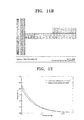
- FIGS. 11A and 11B are views illustrating a temperature distribution of a convective assembly system when conduction and radiation are applied to the convective assembly system.
- FIG. 11A shows/the temperature distribution of Case 1 due to radiant heat
- FIG. 11B shows the temperature distribution of Case 2 due to conductive heat.
- FIG. 12 is a view illustrating a temperature distribution according to a position of a substrate, according to an embodiment of the present invention.
- the temperature distribution of Case 1 due to the radiant heat and Case 2 due to the conductive heat which illustrates the temperature in accordance with a position in the length (x) of the substrate, i.e., on the abscissa.
- FIG. 13 illustrates an exemplary sectional structure of a convective assembly apparatus for a nano-particle array according to another embodiment of the present invention.
- a fixed cover 210 and a sliding substrate 220 that is able to be moved at a constant speed are arranged to face each other spaced apart at a predetermined distance to allow movement relative to each other.
- the fixed cover 210 includes an opening 215 in a flare shape, for supplying a colloidal solution.
- the opening 215 is connected to a solution tank (not shown) through a pipe (not shown), for continuously supplying the colloidal solution in the space between the fixed cover 210 and the sliding substrate 220 when the sliding substrate 220 moves relative to the fixed cover 210 .
- the sliding substrate 220 moves at a constant speed by a driving roller 225 rotating the sliding substrate 220 in one direction.
- a heating unit 250 for supplying a desired radiant heat to the front portion of the colloidal solution may be positioned above the sliding substrate 220 as shown in the FIG. 13 .
- the heat unit 250 such as an electrothermal wire, may be positioned under the sliding substrate as shown.
- the heating unit 250 locally heats the front portion of the colloidal solution. Then, nano-particles are uniformly arrayed on the sliding substrate 220 due to the vaporization of the solvent and the Marangoni flow.
- an exhaust passage 260 allows the vaporized gas of the solvent to be exhausted.
- FIG. 14 is a plan view illustrating a pattern of the nano-particle array obtained by the method according to the present invention.
- the nano-particles 10 enclosed by the coating layer 20 are adhered closely to one another and arrayed closely together.
- FIGS. 15A and 15B are sectional views illustrating a post-process performed after the nano-particles 10 are arrayed on the mobile substrate 120 using the convective assembly apparatus, according to an embodiment of the present invention.
- the post-process may be performed as desired.
- a part of the coating layer 20 formed on the surface of the nano-particles 10 is removed by dry etching such as plasma etching.
- plasma etching a vertically accelerated plasma ion particle can be used to selectively etch a portion of the coating layer 20 between the nano-particles 10 .
- An etching mask can be used if desired.
- the coating layer 20 is removed, the nano-particles 10 are arrayed in regular intervals.
- the thickness of the coating layer 20 is controlled to control the distance between the nano-particles 10 . This means that the nano-particles 10 can be uniformly arrayed as required.
- FIG. 15B illustrates when the nano-particles 10 are on the substrate 120 by performing a wet etching and a pyrolysis process.
- the wet etching process is chemically performed by using an etching solution that selectively reacts with certain species in the coating layer.
- the pyrolysis process burns selected residual portions, which are to be removed, after the wet-etching process.
- the nano-particles 10 are uniformly arrayed on a large area substrate by controlling the thickness of the coating layer.
- the nano-particles having a particle size from a few to several tens of nanometers are uniformly or regularly arrayed. Since a pre-process of forming a coating layer on the nano-particles is performed, the convective assembly can be applied with respect to the nano-particles having a particle size from a few to several tens of nanometers with the advantage that a nano-particle monolayer or multilayer can be obtained through a relatively simple process.
- the array of nano-particles is uniformly arrayed on a large area substrate, and can be formed by suitably controlling the thickness of the coating layer of the nano-particles.
- the method of locally heating the front portion of the colloidal solution by conduction or radiation is used for vaporizing the colloidal solution including the nano-particles, it is possible to structurally prevent the nano-particle array from splitting due to any physical impact. Since only the front portion of the colloid solution is intensively heated, a flow of the colloidal solution can be generated to benefit the nano-particle array.
Landscapes
- Engineering & Computer Science (AREA)
- Chemical & Material Sciences (AREA)
- Nanotechnology (AREA)
- Crystallography & Structural Chemistry (AREA)
- Physics & Mathematics (AREA)
- Inorganic Chemistry (AREA)
- Composite Materials (AREA)
- Condensed Matter Physics & Semiconductors (AREA)
- General Physics & Mathematics (AREA)
- Materials Engineering (AREA)
- Mathematical Physics (AREA)
- Theoretical Computer Science (AREA)
- Manufacturing & Machinery (AREA)
- Application Of Or Painting With Fluid Materials (AREA)
Abstract
Description
Claims (16)
Priority Applications (1)
| Application Number | Priority Date | Filing Date | Title |
|---|---|---|---|
| US13/223,374 US20110308455A1 (en) | 2006-02-08 | 2011-09-01 | Method of forming nano-particle array by convective assembly, and convective assembly apparatus for the same |
Applications Claiming Priority (2)
| Application Number | Priority Date | Filing Date | Title |
|---|---|---|---|
| KR10-2006-0012033 | 2006-02-08 | ||
| KR1020060012033A KR101281165B1 (en) | 2006-02-08 | 2006-02-08 | Method to form nano-particle array by convective assembly and a convective assembly apparatus for the same |
Related Child Applications (1)
| Application Number | Title | Priority Date | Filing Date |
|---|---|---|---|
| US13/223,374 Division US20110308455A1 (en) | 2006-02-08 | 2011-09-01 | Method of forming nano-particle array by convective assembly, and convective assembly apparatus for the same |
Publications (2)
| Publication Number | Publication Date |
|---|---|
| US20070190240A1 US20070190240A1 (en) | 2007-08-16 |
| US8097304B2 true US8097304B2 (en) | 2012-01-17 |
Family
ID=38368880
Family Applications (2)
| Application Number | Title | Priority Date | Filing Date |
|---|---|---|---|
| US11/567,926 Expired - Fee Related US8097304B2 (en) | 2006-02-08 | 2006-12-07 | Method of forming nano-particle array by convective assembly, and convective assembly apparatus for the same |
| US13/223,374 Abandoned US20110308455A1 (en) | 2006-02-08 | 2011-09-01 | Method of forming nano-particle array by convective assembly, and convective assembly apparatus for the same |
Family Applications After (1)
| Application Number | Title | Priority Date | Filing Date |
|---|---|---|---|
| US13/223,374 Abandoned US20110308455A1 (en) | 2006-02-08 | 2011-09-01 | Method of forming nano-particle array by convective assembly, and convective assembly apparatus for the same |
Country Status (2)
| Country | Link |
|---|---|
| US (2) | US8097304B2 (en) |
| KR (1) | KR101281165B1 (en) |
Families Citing this family (6)
| Publication number | Priority date | Publication date | Assignee | Title |
|---|---|---|---|---|
| KR100634510B1 (en) * | 2004-09-06 | 2006-10-13 | 삼성전자주식회사 | Pyrolysis furnace with flow path control |
| TWI460305B (en) * | 2010-11-30 | 2014-11-11 | Ind Tech Res Inst | Apparatus for chemical bath deposition |
| US8951445B2 (en) | 2011-04-14 | 2015-02-10 | International Business Machines Corporation | Bridging arrangement and method for manufacturing a bridging arrangement |
| TW201251094A (en) * | 2011-06-07 | 2012-12-16 | Hon Hai Prec Ind Co Ltd | Electrode of dye-sensitized solar cells manufacturing equipment |
| KR102169064B1 (en) * | 2019-03-18 | 2020-10-22 | 서울시립대학교 산학협력단 | Method for manufacturing colloidal metal nanoparticle assembly through light-induced photothermal convection |
| CN110176541A (en) * | 2019-06-09 | 2019-08-27 | 苏州大学 | A kind of vulcanized lead Colloidal Quantum Dots solar battery and preparation method based on convection current assembling sedimentation |
Citations (13)
| Publication number | Priority date | Publication date | Assignee | Title |
|---|---|---|---|---|
| KR20010019448A (en) | 1999-08-27 | 2001-03-15 | 윤종용 | Method and apparatus for image data segmentation |
| US20020023894A1 (en) * | 2000-08-23 | 2002-02-28 | Robert Rossi | Surface preparation of substances for continuous convective assembly of fine particles |
| KR20020020474A (en) | 2000-09-09 | 2002-03-15 | 박호군 | Method of aligning quantum dots and an semiconductor device fabricated thereby |
| US20020078892A1 (en) * | 2000-12-27 | 2002-06-27 | Nobuyuki Takahashi | Substrate processing device and through-chamber |
| US20020176988A1 (en) * | 1999-07-02 | 2002-11-28 | Medwick Paul A. | Light-transmitting and/or coated article with removable protective coating and methods of making the same |
| US20030166297A1 (en) * | 1999-10-06 | 2003-09-04 | Surromed, Inc. | Surface enhanced spectroscopy-active composite nanoparticles |
| US20040005258A1 (en) * | 2001-12-12 | 2004-01-08 | Fonash Stephen J. | Chemical reactor templates: sacrificial layer fabrication and template use |
| KR20040059588A (en) | 2002-12-27 | 2004-07-06 | 삼성전자주식회사 | Method for preparing a Quantum dot Thin Film using Dithiol Compound |
| KR20040075116A (en) | 2003-02-20 | 2004-08-27 | 재단법인서울대학교산학협력재단 | A method to form the uniform monolayer or multilayer consisting of quantum dot (nanoparticle) array on the wafer by using multiple adsorption phenomena in dip-coating process |
| KR20050000354A (en) | 2003-06-24 | 2005-01-03 | 주식회사 케이티앤지 | Healthy foods containing butterbur extract for memory ability improvement |
| US20050000816A1 (en) * | 2003-07-04 | 2005-01-06 | Sentelic Corporation | Method of making a microstructure using a circuit board |
| KR20050075073A (en) | 2004-01-15 | 2005-07-20 | 재단법인서울대학교산학협력재단 | A method of forming quantum layer and patterned structure by multiple dip-coating processes |
| US20060003097A1 (en) * | 2003-08-06 | 2006-01-05 | Andres Ronald P | Fabrication of nanoparticle arrays |
Family Cites Families (11)
| Publication number | Priority date | Publication date | Assignee | Title |
|---|---|---|---|---|
| US4987851A (en) * | 1988-01-12 | 1991-01-29 | Kabushiki Kaisha Toshiba | Apparatus for forming organic thin film |
| GB2281309B (en) * | 1993-08-27 | 1997-04-23 | Boc Group Plc | A method of galvanising |
| JP2828386B2 (en) * | 1993-08-31 | 1998-11-25 | 科学技術振興事業団 | Manufacturing method of fine particle thin film |
| US6599560B1 (en) * | 1997-10-30 | 2003-07-29 | Fsi International, Inc. | Liquid coating device with barometric pressure compensation |
| KR20020094479A (en) * | 2001-06-12 | 2002-12-18 | 서울대학교 공과대학 교육연구재단 | A method of array of quantum dots on the wafer and a apparatus thereof |
| EP1462746B1 (en) * | 2003-03-26 | 2013-05-08 | FUJIFILM Corporation | Drying method and drying apparatus for coating layer |
| PL3120983T5 (en) * | 2003-06-24 | 2024-04-22 | Aspen Aerogels, Inc. | Continuous sheet of gel material and continuous sheet of aerogel material |
| US20050042387A1 (en) * | 2003-08-21 | 2005-02-24 | 3M Innovative Properties Company | Filament coating process and apparatus |
| TWI417564B (en) * | 2005-02-21 | 2013-12-01 | Dainippon Printing Co Ltd | Manufacturing method and manufacturing apparatus for optical laminate |
| US7339439B2 (en) * | 2005-07-18 | 2008-03-04 | Atmel Corporation | Voltage-controlled oscillator with multi-phase realignment of asymmetric stages |
| US7520933B2 (en) * | 2006-08-30 | 2009-04-21 | Korea Advanced Institute Of Science And Technology | Method for manufacturing colloidal crystals via confined convective assembly |
-
2006
- 2006-02-08 KR KR1020060012033A patent/KR101281165B1/en not_active Expired - Fee Related
- 2006-12-07 US US11/567,926 patent/US8097304B2/en not_active Expired - Fee Related
-
2011
- 2011-09-01 US US13/223,374 patent/US20110308455A1/en not_active Abandoned
Patent Citations (13)
| Publication number | Priority date | Publication date | Assignee | Title |
|---|---|---|---|---|
| US20020176988A1 (en) * | 1999-07-02 | 2002-11-28 | Medwick Paul A. | Light-transmitting and/or coated article with removable protective coating and methods of making the same |
| KR20010019448A (en) | 1999-08-27 | 2001-03-15 | 윤종용 | Method and apparatus for image data segmentation |
| US20030166297A1 (en) * | 1999-10-06 | 2003-09-04 | Surromed, Inc. | Surface enhanced spectroscopy-active composite nanoparticles |
| US20020023894A1 (en) * | 2000-08-23 | 2002-02-28 | Robert Rossi | Surface preparation of substances for continuous convective assembly of fine particles |
| KR20020020474A (en) | 2000-09-09 | 2002-03-15 | 박호군 | Method of aligning quantum dots and an semiconductor device fabricated thereby |
| US20020078892A1 (en) * | 2000-12-27 | 2002-06-27 | Nobuyuki Takahashi | Substrate processing device and through-chamber |
| US20040005258A1 (en) * | 2001-12-12 | 2004-01-08 | Fonash Stephen J. | Chemical reactor templates: sacrificial layer fabrication and template use |
| KR20040059588A (en) | 2002-12-27 | 2004-07-06 | 삼성전자주식회사 | Method for preparing a Quantum dot Thin Film using Dithiol Compound |
| KR20040075116A (en) | 2003-02-20 | 2004-08-27 | 재단법인서울대학교산학협력재단 | A method to form the uniform monolayer or multilayer consisting of quantum dot (nanoparticle) array on the wafer by using multiple adsorption phenomena in dip-coating process |
| KR20050000354A (en) | 2003-06-24 | 2005-01-03 | 주식회사 케이티앤지 | Healthy foods containing butterbur extract for memory ability improvement |
| US20050000816A1 (en) * | 2003-07-04 | 2005-01-06 | Sentelic Corporation | Method of making a microstructure using a circuit board |
| US20060003097A1 (en) * | 2003-08-06 | 2006-01-05 | Andres Ronald P | Fabrication of nanoparticle arrays |
| KR20050075073A (en) | 2004-01-15 | 2005-07-20 | 재단법인서울대학교산학협력재단 | A method of forming quantum layer and patterned structure by multiple dip-coating processes |
Non-Patent Citations (1)
| Title |
|---|
| Mun Ho Kim, Sang Hyuk Im, and O Ok Park; Rapid Fabrication of Two- and Three-Dimensional Colloidal Crystal Films via Confined Convective Assembly; Advanced Functional Material 2005, 15, 1329-1335; Received Dec. 22, 2005; Final version: Mar. 28, 2005. |
Also Published As
| Publication number | Publication date |
|---|---|
| US20110308455A1 (en) | 2011-12-22 |
| KR20070080681A (en) | 2007-08-13 |
| US20070190240A1 (en) | 2007-08-16 |
| KR101281165B1 (en) | 2013-07-02 |
Similar Documents
| Publication | Publication Date | Title |
|---|---|---|
| US20110308455A1 (en) | Method of forming nano-particle array by convective assembly, and convective assembly apparatus for the same | |
| US20090130427A1 (en) | Nanomaterial facilitated laser transfer | |
| US20120015112A1 (en) | Method of fabricating pattern | |
| Armon et al. | Continuous nanoparticle assembly by a modulated photo-induced microbubble for fabrication of micrometric conductive patterns | |
| KR101291671B1 (en) | Thermal control of deposition in dip pen nanolithography | |
| Watanabe et al. | Spontaneous formation of cluster array of gold particles by convective self-assembly | |
| JP5141506B2 (en) | Plasmonic crystal surface emitter, image display device, and illumination device | |
| US9625381B2 (en) | Sensor including nanostructure and method for fabricating the same | |
| US7018944B1 (en) | Apparatus and method for nanoscale pattern generation | |
| US20100166976A1 (en) | Method of manufacturing core-shell nanostructure | |
| US9768401B2 (en) | Single electron transistor | |
| Liang et al. | Femtosecond laser patterning wettability‐assisted PDMS for fabrication of flexible silver nanowires electrodes | |
| CN101910452A (en) | Method and system for continuous or semi-continuous laser deposition | |
| US20150177139A1 (en) | Sensor including flexible nanostructure and method for fabricating the same | |
| Ritacco et al. | Insight into diffusive and convective processes affecting gold nanoparticles microclustering by multiphoton photoreduction | |
| JP6041145B2 (en) | Method for producing oxide dot pattern | |
| US7402445B2 (en) | Method of forming micro-structures and nano-structures | |
| JP4170619B2 (en) | Method for producing fine particle structure | |
| Okoshi et al. | Fabrication of silicone rubber-based biochip for disinfection under deep-UV light by ArF excimer laser-induced photodissociation | |
| US20110305838A1 (en) | Method of production of a deposit of nanoparticles with increased adhesion and device for implementation of such a method | |
| US11813676B2 (en) | Migration of nano metals in semisolid and solid matrix under the influence of selectively triggered heterogeneous nucleation and growth | |
| TW200813504A (en) | Electromagnetic waveguide | |
| Miller et al. | Templated self-assembly of glass microspheres into ordered two-dimensional arrays under dry conditions | |
| US7799707B2 (en) | Method of forming gated, self-aligned micro-structures and nano structures | |
| US20240375348A1 (en) | Printhead, system and method for direct write vapor deposition |
Legal Events
| Date | Code | Title | Description |
|---|---|---|---|
| AS | Assignment |
Owner name: SAMSUNG ELECTRONICS CO., LTD., KOREA, REPUBLIC OF Free format text: ASSIGNMENT OF ASSIGNORS INTEREST;ASSIGNORS:CHOI, HYUK-SOON;LEE, HYO-SUG;KOO, JUNE-MO;AND OTHERS;REEL/FRAME:018596/0614 Effective date: 20061123 |
|
| ZAAA | Notice of allowance and fees due |
Free format text: ORIGINAL CODE: NOA |
|
| ZAAB | Notice of allowance mailed |
Free format text: ORIGINAL CODE: MN/=. |
|
| ZAAA | Notice of allowance and fees due |
Free format text: ORIGINAL CODE: NOA |
|
| ZAAB | Notice of allowance mailed |
Free format text: ORIGINAL CODE: MN/=. |
|
| FEPP | Fee payment procedure |
Free format text: PAYOR NUMBER ASSIGNED (ORIGINAL EVENT CODE: ASPN); ENTITY STATUS OF PATENT OWNER: LARGE ENTITY |
|
| STCF | Information on status: patent grant |
Free format text: PATENTED CASE |
|
| FPAY | Fee payment |
Year of fee payment: 4 |
|
| MAFP | Maintenance fee payment |
Free format text: PAYMENT OF MAINTENANCE FEE, 8TH YEAR, LARGE ENTITY (ORIGINAL EVENT CODE: M1552); ENTITY STATUS OF PATENT OWNER: LARGE ENTITY Year of fee payment: 8 |
|
| FEPP | Fee payment procedure |
Free format text: MAINTENANCE FEE REMINDER MAILED (ORIGINAL EVENT CODE: REM.); ENTITY STATUS OF PATENT OWNER: LARGE ENTITY |
|
| LAPS | Lapse for failure to pay maintenance fees |
Free format text: PATENT EXPIRED FOR FAILURE TO PAY MAINTENANCE FEES (ORIGINAL EVENT CODE: EXP.); ENTITY STATUS OF PATENT OWNER: LARGE ENTITY |
|
| STCH | Information on status: patent discontinuation |
Free format text: PATENT EXPIRED DUE TO NONPAYMENT OF MAINTENANCE FEES UNDER 37 CFR 1.362 |
|
| FP | Lapsed due to failure to pay maintenance fee |
Effective date: 20240117 |