US8092029B2 - Lens module comprising at least one exchangeable optical element - Google Patents
Lens module comprising at least one exchangeable optical element Download PDFInfo
- Publication number
- US8092029B2 US8092029B2 US11/722,595 US72259505A US8092029B2 US 8092029 B2 US8092029 B2 US 8092029B2 US 72259505 A US72259505 A US 72259505A US 8092029 B2 US8092029 B2 US 8092029B2
- Authority
- US
- United States
- Prior art keywords
- gas
- optical element
- lens
- lens module
- housing
- Prior art date
- Legal status (The legal status is an assumption and is not a legal conclusion. Google has not performed a legal analysis and makes no representation as to the accuracy of the status listed.)
- Expired - Fee Related, expires
Links
Images


Classifications
-
- G—PHYSICS
- G03—PHOTOGRAPHY; CINEMATOGRAPHY; ANALOGOUS TECHNIQUES USING WAVES OTHER THAN OPTICAL WAVES; ELECTROGRAPHY; HOLOGRAPHY
- G03F—PHOTOMECHANICAL PRODUCTION OF TEXTURED OR PATTERNED SURFACES, e.g. FOR PRINTING, FOR PROCESSING OF SEMICONDUCTOR DEVICES; MATERIALS THEREFOR; ORIGINALS THEREFOR; APPARATUS SPECIALLY ADAPTED THEREFOR
- G03F7/00—Photomechanical, e.g. photolithographic, production of textured or patterned surfaces, e.g. printing surfaces; Materials therefor, e.g. comprising photoresists; Apparatus specially adapted therefor
- G03F7/20—Exposure; Apparatus therefor
-
- G—PHYSICS
- G02—OPTICS
- G02B—OPTICAL ELEMENTS, SYSTEMS OR APPARATUS
- G02B27/00—Optical systems or apparatus not provided for by any of the groups G02B1/00 - G02B26/00, G02B30/00
- G02B27/0006—Optical systems or apparatus not provided for by any of the groups G02B1/00 - G02B26/00, G02B30/00 with means to keep optical surfaces clean, e.g. by preventing or removing dirt, stains, contamination, condensation
-
- G—PHYSICS
- G02—OPTICS
- G02B—OPTICAL ELEMENTS, SYSTEMS OR APPARATUS
- G02B7/00—Mountings, adjusting means, or light-tight connections, for optical elements
- G02B7/02—Mountings, adjusting means, or light-tight connections, for optical elements for lenses
- G02B7/14—Mountings, adjusting means, or light-tight connections, for optical elements for lenses adapted to interchange lenses
-
- G—PHYSICS
- G03—PHOTOGRAPHY; CINEMATOGRAPHY; ANALOGOUS TECHNIQUES USING WAVES OTHER THAN OPTICAL WAVES; ELECTROGRAPHY; HOLOGRAPHY
- G03F—PHOTOMECHANICAL PRODUCTION OF TEXTURED OR PATTERNED SURFACES, e.g. FOR PRINTING, FOR PROCESSING OF SEMICONDUCTOR DEVICES; MATERIALS THEREFOR; ORIGINALS THEREFOR; APPARATUS SPECIALLY ADAPTED THEREFOR
- G03F7/00—Photomechanical, e.g. photolithographic, production of textured or patterned surfaces, e.g. printing surfaces; Materials therefor, e.g. comprising photoresists; Apparatus specially adapted therefor
- G03F7/70—Microphotolithographic exposure; Apparatus therefor
- G03F7/70058—Mask illumination systems
- G03F7/7015—Details of optical elements
-
- G—PHYSICS
- G03—PHOTOGRAPHY; CINEMATOGRAPHY; ANALOGOUS TECHNIQUES USING WAVES OTHER THAN OPTICAL WAVES; ELECTROGRAPHY; HOLOGRAPHY
- G03F—PHOTOMECHANICAL PRODUCTION OF TEXTURED OR PATTERNED SURFACES, e.g. FOR PRINTING, FOR PROCESSING OF SEMICONDUCTOR DEVICES; MATERIALS THEREFOR; ORIGINALS THEREFOR; APPARATUS SPECIALLY ADAPTED THEREFOR
- G03F7/00—Photomechanical, e.g. photolithographic, production of textured or patterned surfaces, e.g. printing surfaces; Materials therefor, e.g. comprising photoresists; Apparatus specially adapted therefor
- G03F7/70—Microphotolithographic exposure; Apparatus therefor
- G03F7/708—Construction of apparatus, e.g. environment aspects, hygiene aspects or materials
- G03F7/70808—Construction details, e.g. housing, load-lock, seals or windows for passing light in or out of apparatus
- G03F7/70825—Mounting of individual elements, e.g. mounts, holders or supports
-
- G—PHYSICS
- G03—PHOTOGRAPHY; CINEMATOGRAPHY; ANALOGOUS TECHNIQUES USING WAVES OTHER THAN OPTICAL WAVES; ELECTROGRAPHY; HOLOGRAPHY
- G03F—PHOTOMECHANICAL PRODUCTION OF TEXTURED OR PATTERNED SURFACES, e.g. FOR PRINTING, FOR PROCESSING OF SEMICONDUCTOR DEVICES; MATERIALS THEREFOR; ORIGINALS THEREFOR; APPARATUS SPECIALLY ADAPTED THEREFOR
- G03F7/00—Photomechanical, e.g. photolithographic, production of textured or patterned surfaces, e.g. printing surfaces; Materials therefor, e.g. comprising photoresists; Apparatus specially adapted therefor
- G03F7/70—Microphotolithographic exposure; Apparatus therefor
- G03F7/708—Construction of apparatus, e.g. environment aspects, hygiene aspects or materials
- G03F7/70908—Hygiene, e.g. preventing apparatus pollution, mitigating effect of pollution or removing pollutants from apparatus
- G03F7/70933—Purge, e.g. exchanging fluid or gas to remove pollutants
Definitions
- the invention relates to a lens module comprising at least one exchangeable optical element.
- a lens module is understood as meaning part of a projection lens or an illuminating lens for semiconductor lithography or else the entire lens.
- the invention also relates to a method for flushing a receiving region of an optical element.
- the exchangeable optical elements referred to may be used both in the projection lens and in the illuminating system of a projection exposure machine.
- the present invention is therefore based on the object of providing a lens module, in particular a projection lens for semiconductor lithography, with which no contamination is introduced after an optical element is exchanged and re-fitted, and rapid reuse is made possible.
- At least one gas exchange device being arranged in a region of the exchangeable optical element in such a way that a receiving region for the exchangeable optical element can be flushed during the exchange of the optical element.
- the at least one gas exchange device by which the receiving region of the optical element is flushed during the exchange, i.e. in the opened state of the lens module, allows contamination in the interior of the lens module during the exchange of the optical element to be avoided, so that much less flushing time is necessary after the closing of the lens module.
- the consequently reduced downtime of the machine has the effect that an exchange of the optical element is more acceptable.
- the risk of internal contaminations during the exchange of the optical element on account of reduced effectiveness of the exchangeable optical element can be significantly reduced by the flushing according to the invention of the receiving region for the optical element.
- An advantage of this solution is that the projection exposure machine can be optimized in a very short time for this respectively chosen application, so that the machine can also be operated with a high throughput in the case of small batches for a specific type of device.
- the proposed solution effectively reduces the risk of contamination by the two mechanisms described below: during the exchange of the optical elements, contaminations can diffuse into the lens module as a result of it being opened for a short time. This diffusion even takes place when the lens module is under increased pressure in comparison with ambient pressure. Moreover, the movement of the exchangeable optical element can cause gas to be introduced from the ambience by the effects of suction and turbulence.
- contamination adsorbed on the exchangeable element in particular hydrocarbons, which may be deposited on it during storage.
- the at least one gas exchange device is formed as a gas inlet device in such a way that a laminar gas stream is obtained, completely or virtually preventing inward diffusion of contaminations from the ambient air during the exchange of the optical element.
- the at least one gas inlet device has a grating device with at least one grating, with preference two or more gratings, to produce the laminar gas stream.
- a laminar gas stream has the effect of avoiding turbulences, and consequently effectively removing or keeping away from the interior of the lens module contaminations which could diffuse into the lens module during the exchange of the optical element.
- FIG. 1 shows a basic representation of a projection exposure machine for semiconductor lithography, which can be used for exposing structures on wafers coated with photosensitive materials;
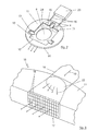
- FIG. 2 shows a perspective basic diagram of a mount of a lens housing in which an exchangeable optical element is arranged
- FIG. 3 shows a perspective representation of a gas inlet device according to the invention
- FIG. 4 shows a perspective representation of an alternative gas inlet device according to the invention
- FIG. 5 shows a basic representation of a lens module with a number of exchangeable optical elements for a further projection exposure machine
- FIG. 6 shows a basic representation of a lens module with a gas outlet device in a region of the lens housing that lies opposite a push-in opening for the optical element
- FIG. 7 shows a basic representation of a lens module with a further gas inlet device on the side of the housing mount opposite the push-in opening;
- FIG. 8 shows a basic representation of a lens module with a further gas inlet device on the side of the push-in opening in the housing mount;
- FIG. 9 shows a basic representation of a lens module with a gas lock for keeping the optical element
- FIG. 10 shows a basic representation of a lens module with a gas inlet device with a valve which can be activated by means of a control device;
- FIG. 11 shows a basic representation of a lens module, the inner space of the lens housing being designed in such a way that contamination from the receiving region into adjacent spaces in the lens housing is largely suppressed;
- FIG. 12 shows an alternative arrangement of the element to be exchanged in the lens module.
- a projection exposure machine 1 for semiconductor lithography serves for exposing structures on a substrate which is coated with photosensitive materials, generally consists predominantly of silicon and is referred to as a wafer 2 , for the production of semiconductor devices, such as for example computer chips.
- the projection exposure machine 1 in this case substantially comprises an illuminating device 3 , a device 4 for receiving and exactly positioning a mask provided with a grating-like structure, known as a reticle 5 , by which the later structures on the wafer 2 are determined, a device 6 for securing, advancing and exactly positioning the wafer 2 and a projection lens 7 .
- the basic functional principle provides in this case that the structures introduced into the reticle 5 are exposed on the wafer 2 , in particular with a reduction in the size of the structures to one third or less of the original size.
- the requirements to be imposed on the projection exposure machine 1 , in particular on the projection lens 7 , with regard to the resolution in this case lie in the range of just a few nanometers.
- said wafer is advanced, so that a multiplicity of individual fields, each with the structure determined by the reticle 5 , are exposed on the same wafer 2 .
- said wafer is removed from the projection exposure machine 1 and subjected to a plurality of chemical treatment steps, generally removing material by etching. If appropriate, a number of these exposure and treatment steps are passed through one after the other, until a multiplicity of computer chips are created on the wafer 2 .
- the illuminating device 3 provides a projection beam 8 , for example light or similar electromagnetic radiation, required for the imaging of the reticle 5 on the wafer 2 .
- a laser or the like may be used as the source of this radiation.
- the radiation is supplied to the illuminating device 3 by means of optical elements, so that the projection beam 8 has the desired properties with regard to diameter, polarization and the like when it impinges on the reticle 5 .
- An image of the reticle 5 is produced by means of the projection beam 8 and is transmitted by the projection lens 7 in an appropriately reduced size onto the wafer 2 , as already explained above.
- the projection lens 7 in this case comprises a multiplicity of individual refractive and/or diffractive elements, such as for example lenses, mirrors, prisms, end plates or the like.
- At least one optical element 9 which is formed as an exchangeable optical element is mounted in a mount 10 .
- the optical element 9 here a lens
- the mount 10 with the optical element 9 is in turn mounted in a housing mount 11 , which is part of a lens housing 12 .
- the lens housing is part of the lens module or forms the lens module.
- the housing mount 11 in this case forms part of the outer circumference of the lens housing 12 .
- exchangeable optical elements may likewise be provided in the projection lens 7 , the optical element 9 in the pupil plane being assumed hereafter.
- the exchangeable optical element 9 is perspectively represented.
- the optical element 9 mounted in the projection lens 7 in a receiving region 10 ′ provided for it, is connected to the mount 10 for example by means of small supporting feet.
- the mount 10 is connected to the latter by means of three fastening elements 13 .
- the housing mount 11 of the lens housing 12 comprises a ring, in particular a steel ring, in which a push-in opening 14 is made for the insertion of the mount 10 with the optical element 9 .
- the push-in opening 14 is made, in particular milled, in the housing mount 11 of the lens housing 12 , in order in this way to ensure simple exchange of the optical element 9 .
- the fastening elements 13 may be formed as adjustable fastening elements, for example as manipulators, in order to mount the mount 10 with the optical element 9 exactly and centered in the housing mount 11 of the lens housing 12 .
- two gas inlet devices 15 are respectively provided in a region opposite the push-in opening 14 for the optical element 9 .
- one of the two gas inlet devices 15 is represented in more detail in an enlarged form.
- the regions in which a gas inlet device 15 is respectively arranged in the housing mount 11 of the lens housing 12 are identified in FIG. 2 by an “X”.
- a gas stream is supplied by way of at least one gas inlet line 16 to the gas inlet devices 15 , which produce a laminar gas stream, a gas inlet line 16 for each gas inlet device 15 being represented in FIG. 2 .
- the gas stream introduced into the gas inlet devices 15 from outside the projection lens 7 is supplied to the gas inlet devices 15 by a gas supply device 23 by way of the gas inlet lines 16 .
- the laminar gas stream represented by the arrows is conducted in the direction of the push-in opening 14 , whereby a flushing of the receiving region 10 ′ of the mount 10 is performed, and so contaminations in the interior of the projection lens 7 are avoided during the exchange of the mount 10 .
- the gas inlet device 15 represented in FIG. 3 has a grating device 17 at the inlet into the receiving region 10 ′.
- Said grating device is provided with a number of gratings 18 one behind the other and offset in relation to one another, which are only indicated here, in order to produce a laminar gas stream.
- a number of gratings 18 one behind the other and offset in relation to one another, which are only indicated here, in order to produce a laminar gas stream.
- at least three gratings 18 should be provided, as shown by the basic representation in FIG. 3 .
- it is self-evidently also possible to provide only one grating 18 in the grating device 17 if at least one largely laminar gas stream can be ensured with it.
- FIG. 3 shows the gas inlet line 16 for introducing the gas stream, which is represented here by an arrow 19 .
- Either high-purity nitrogen or noble gas or gas mixtures of such inert gases as nitrogen or noble gases may be used as the gas; the same gas that is already used in the interior of the projection lens 7 for flushing the same should advantageously be used.
- the gas pressure of the gas stream that is used should be regulated in such a way that a laminar gas stream is ensured.
- at least one cross-bore 22 is provided in the housing mount 11 of the lens housing 12 .
- a bore device 20 with a multiplicity of bores 21 may be provided in a plate at the end of the bore 22 in the housing mount 11 , in front of the outlet in the receiving region 10 ′, FIG. 4 showing said plurality of bores arranged in a plate 20 ′. Since only the grating device 17 has been replaced by the bore device 20 , and otherwise the same parts as in FIG. 3 are provided, the same designations have also been used.
- the bore device 20 may also have a number of bores 21 one behind the other and offset in relation to one another, which are arranged in plates 20 ′ arranged at a distance from one another.
- a projection lens 7 ′ with a lens housing 12 ′ for a further embodiment of the projection exposure machine 1 is represented in a greatly simplified form.
- the device 4 for receiving and exactly positioning the reticle 5 and the wafer 2 are indicated by dashed lines.
- the projection lens 7 ′ has, beginning at the reticle 5 and proceeding in the radiating direction, a refractive part 31 , an exchangeable deflecting prism 32 , a catadioptric part 33 with a lens 34 and an exchangeable concave deflecting mirror 35 as well as a further refractive part 36 with an exchangeable end element 37 .
- the exchangeable optical elements i.e.
- the deflecting prism 32 , the concave deflecting mirror 35 and the end element 37 , gas inlet devices with gas supply devices 23 and gas inlet lines 16 are arranged in the housing mount (not represented in any more detail), whereby it is possible during the exchange of the optical elements 32 , 35 and 37 for their receiving regions (not represented in detail in FIG. 5 ) to be flushed.
- the gas in the inner space of the lens housing 12 is conducted in such a way that, during the exchange, it flows away through the push-in opening 14 , as represented in FIG. 6 .
- the exchangeable element 9 is at the center of a lens housing 12 , between at least two further optical elements 9 a and 9 b .
- a gas inlet device 41 or 42 is respectively provided at both ends and a gas outlet device 43 is provided in the receiving region 10 ′, which accommodates the element 9 to be exchanged.
- a further gas inlet device 44 is located in the receiving region 10 ′, which accommodates the element 9 to be exchanged.
- a gas outlet device 45 On the side of the lens housing 12 that is facing the push-in opening 14 there is a gas outlet device 45 . It is advantageous in particular in the case of this embodiment that, on account of the arrangement of the gas inlet and outlet devices, a virtually laminar flow in the direction of the push-in opening 14 can form in the interior of the lens housing 12 , allowing contaminations to be efficiently removed from the lens housing 12 .
- FIGS. 6 and 7 Combination of the two embodiments represented in FIGS. 6 and 7 produces the solution described in FIG. 8 .
- a further gas inlet device 46 is present in the vicinity of the receiving region 10 ′, on the side facing the push-in opening. In this way, further significantly increased flushing through of the receiving region 10 ′ is ensured.
- a slight positive pressure of 50 to 1000 Pa in relation to the ambience usually prevails in the inner space of the lens housing 12 . If an opening is then created to exchange the exchangeable element 9 , this positive pressure breaks down virtually completely, unless the gas supply is designed for a short-term delivery of extreme amounts of gas. However, this would lead to undesired side effects, such as for example a drop in pressure in the lines. For example, with a positive pressure of 100 Pa, 4500 l/min of flushing gas would flow through an opening of 100 ⁇ 2 mm in a 5 mm thick housing wall.
- FIG. 9 the exchangeable optical element 9 is brought into a gas lock 47 , in which there prevails a pressure that is greater than the ambient pressure but less than or equal to the desired positive pressure in the lens housing 12 . It is introduced into the gas lock 47 through the lock opening 60 and, from there, is introduced into the lens housing 12 through the push-in opening 14 .
- a number of exchangeable elements 9 c , 9 d , 9 e may be stored in the gas lock 47 .
- the gas lock 47 is flushed with the same gas as the lens housing 12 and has its own gas inlet device 48 and a gas outlet device 49 .
- Any other gas inlet device may also serve as the gas inlet device for the gas supply; similarly, it is conceivable to close a gas outlet device during a changing operation.
- this additional gas stream is introduced into the receiving region 10 ′and switched on at the same time as or in temporal correlation with the motorized actuation of the push-in opening 14 in the lens housing 12 .
- the receiving region 10 ′ is continuously flushed in the direction of the exchange opening during the changing operation. Since the gas flow is only required for the duration of the exchange, the gas flow can be a multiple of the gas flow conventionally used for flushing the lens housing 12 . In this case, it is advantageous if 95%, with preference 99%, of the positive operating pressure is achieved in the lens housing within 5 min, with preference within 30 s, after the change of the optical element, in particular after the closing of the push-in opening 14 .
- FIG. 11 shows a solution by which the inward diffusion of contamination from the receiving region 10 ′ into adjacent gas spaces 55 a and 55 b can be restricted. Even if a higher pressure prevails in the adjacent gas spaces 55 a , 55 b than in the receiving region 10 ′, contamination can penetrate into them by diffusion.
- the contamination of the adjacent gas spaces 55 a , 55 b is restricted by the gap between the adjacent gas spaces 55 a , 55 b and the receiving region 10 ′ being provided with a suitable geometry.
- a peripheral gas seal 56 a , 56 b may be realized between the optical elements 9 a , 9 b and the inner wall of the lens housing 12 .
- a gas seal is understood as meaning an at least partially open sealing gap in which a sealing effect is achieved with respect to the ambience by an opposing gas stream.
- FIG. 11 the preferred direction of flow of the flushing gas is indicated by the arrows 75 a,b,c,d.
- H 2 O as the contamination
- N 2 as the flushing gas
Landscapes
- Physics & Mathematics (AREA)
- General Physics & Mathematics (AREA)
- Epidemiology (AREA)
- Health & Medical Sciences (AREA)
- Public Health (AREA)
- Engineering & Computer Science (AREA)
- Environmental & Geological Engineering (AREA)
- Optics & Photonics (AREA)
- Life Sciences & Earth Sciences (AREA)
- Atmospheric Sciences (AREA)
- Exposure Of Semiconductors, Excluding Electron Or Ion Beam Exposure (AREA)
- Exposure And Positioning Against Photoresist Photosensitive Materials (AREA)
- Optical Couplings Of Light Guides (AREA)
Abstract
Description
-
- where
- u=flow velocity of the gas in the gap
- L=length of the gap in the direction of flow
- D=diffusion coefficient of the gas
- C=here concentration in the
gas space 55 a - C0=here concentration in the receiving
region 10′
Claims (37)
Priority Applications (2)
| Application Number | Priority Date | Filing Date | Title |
|---|---|---|---|
| US11/722,595 US8092029B2 (en) | 2004-12-23 | 2005-12-23 | Lens module comprising at least one exchangeable optical element |
| US15/647,254 US20180031827A1 (en) | 2004-12-23 | 2017-07-11 | Lens module comprising at least one exchangeable optical element |
Applications Claiming Priority (3)
| Application Number | Priority Date | Filing Date | Title |
|---|---|---|---|
| US63968404P | 2004-12-23 | 2004-12-23 | |
| PCT/EP2005/013990 WO2006069755A2 (en) | 2004-12-23 | 2005-12-23 | Lens module comprising at least one replaceable optical element |
| US11/722,595 US8092029B2 (en) | 2004-12-23 | 2005-12-23 | Lens module comprising at least one exchangeable optical element |
Related Parent Applications (1)
| Application Number | Title | Priority Date | Filing Date |
|---|---|---|---|
| PCT/EP2005/013990 A-371-Of-International WO2006069755A2 (en) | 2004-12-23 | 2005-12-23 | Lens module comprising at least one replaceable optical element |
Related Child Applications (1)
| Application Number | Title | Priority Date | Filing Date |
|---|---|---|---|
| US13/346,430 Continuation US8376559B2 (en) | 2004-12-23 | 2012-01-09 | Lens module comprising at least one exchangeable optical element |
Publications (2)
| Publication Number | Publication Date |
|---|---|
| US20080137192A1 US20080137192A1 (en) | 2008-06-12 |
| US8092029B2 true US8092029B2 (en) | 2012-01-10 |
Family
ID=35809556
Family Applications (6)
| Application Number | Title | Priority Date | Filing Date |
|---|---|---|---|
| US11/722,595 Expired - Fee Related US8092029B2 (en) | 2004-12-23 | 2005-12-23 | Lens module comprising at least one exchangeable optical element |
| US13/346,430 Expired - Fee Related US8376559B2 (en) | 2004-12-23 | 2012-01-09 | Lens module comprising at least one exchangeable optical element |
| US13/766,174 Expired - Fee Related US8939587B2 (en) | 2004-12-23 | 2013-02-13 | Lens module comprising at least one exchangeable optical element |
| US14/605,232 Expired - Fee Related US9423695B2 (en) | 2004-12-23 | 2015-01-26 | Lens module comprising at least one exchangeable optical element |
| US15/243,397 Expired - Fee Related US9703098B2 (en) | 2004-12-23 | 2016-08-22 | Lens module comprising at least one exchangeable optical element |
| US15/647,254 Abandoned US20180031827A1 (en) | 2004-12-23 | 2017-07-11 | Lens module comprising at least one exchangeable optical element |
Family Applications After (5)
| Application Number | Title | Priority Date | Filing Date |
|---|---|---|---|
| US13/346,430 Expired - Fee Related US8376559B2 (en) | 2004-12-23 | 2012-01-09 | Lens module comprising at least one exchangeable optical element |
| US13/766,174 Expired - Fee Related US8939587B2 (en) | 2004-12-23 | 2013-02-13 | Lens module comprising at least one exchangeable optical element |
| US14/605,232 Expired - Fee Related US9423695B2 (en) | 2004-12-23 | 2015-01-26 | Lens module comprising at least one exchangeable optical element |
| US15/243,397 Expired - Fee Related US9703098B2 (en) | 2004-12-23 | 2016-08-22 | Lens module comprising at least one exchangeable optical element |
| US15/647,254 Abandoned US20180031827A1 (en) | 2004-12-23 | 2017-07-11 | Lens module comprising at least one exchangeable optical element |
Country Status (4)
| Country | Link |
|---|---|
| US (6) | US8092029B2 (en) |
| JP (1) | JP5022912B2 (en) |
| KR (1) | KR101252312B1 (en) |
| WO (1) | WO2006069755A2 (en) |
Families Citing this family (8)
| Publication number | Priority date | Publication date | Assignee | Title |
|---|---|---|---|---|
| US7724351B2 (en) * | 2006-01-30 | 2010-05-25 | Asml Netherlands B.V. | Lithographic apparatus, device manufacturing method and exchangeable optical element |
| DE102006050835A1 (en) * | 2006-10-27 | 2008-05-08 | Carl Zeiss Smt Ag | Method and device for exchanging object parts |
| DE102008028415A1 (en) | 2007-06-22 | 2008-12-24 | Carl Zeiss Smt Ag | Optical assembly, projection exposure apparatus for semiconductor lithography and projection objective |
| NL2008184A (en) | 2011-02-28 | 2012-08-29 | Asml Netherlands Bv | Gas manifold, module for a lithographic apparatus, lithographic apparatus and device manufacturing method. |
| KR101986341B1 (en) * | 2012-03-30 | 2019-06-07 | 삼성전자주식회사 | bi-directional camera module for flip chip bonder used the same |
| CN109283797B (en) * | 2017-07-21 | 2021-04-30 | 上海微电子装备(集团)股份有限公司 | Objective lens protection device, objective lens system and lithographic apparatus |
| CN115327780B (en) | 2017-09-11 | 2025-08-26 | 杜比实验室特许公司 | Modular detachable wearable device for AR/VR/MR |
| DE102021205985A1 (en) | 2021-06-11 | 2022-12-15 | Carl Zeiss Smt Gmbh | Optical arrangement for EUV lithography and method for regenerating a gas-binding component |
Citations (5)
| Publication number | Priority date | Publication date | Assignee | Title |
|---|---|---|---|---|
| US20010026402A1 (en) * | 1998-07-08 | 2001-10-04 | Michael Gerhard | Process for the decontamination of microlithographic projection exposure devices |
| WO2001073825A1 (en) | 2000-03-29 | 2001-10-04 | Nikon Corporation | Aligner, apparatus and method for transferring wafer, microdevice and method for manufacturing the same |
| US20010026355A1 (en) | 2000-03-30 | 2001-10-04 | Nikon Corporation | Exposure apparatus, exposure method, and device manufacturing method |
| DE10121346A1 (en) | 2001-05-02 | 2002-11-07 | Zeiss Carl | Objective, in particular a projection objective for semiconductor lithography |
| JP2004071663A (en) | 2002-08-02 | 2004-03-04 | Canon Inc | Exposure equipment |
Family Cites Families (3)
| Publication number | Priority date | Publication date | Assignee | Title |
|---|---|---|---|---|
| DE10253162B4 (en) * | 2002-11-14 | 2005-11-03 | Infineon Technologies Ag | Method for rinsing an optical lens |
| US7136142B2 (en) * | 2004-05-25 | 2006-11-14 | Asml Netherlands B.V. | Lithographic apparatus having a gas flushing device |
| US7446849B2 (en) * | 2004-07-22 | 2008-11-04 | Asml Netherlands B.V. | Lithographic apparatus and device manufacturing method |
-
2005
- 2005-12-23 KR KR1020077016610A patent/KR101252312B1/en not_active Expired - Fee Related
- 2005-12-23 US US11/722,595 patent/US8092029B2/en not_active Expired - Fee Related
- 2005-12-23 WO PCT/EP2005/013990 patent/WO2006069755A2/en not_active Ceased
- 2005-12-23 JP JP2007547388A patent/JP5022912B2/en not_active Expired - Fee Related
-
2012
- 2012-01-09 US US13/346,430 patent/US8376559B2/en not_active Expired - Fee Related
-
2013
- 2013-02-13 US US13/766,174 patent/US8939587B2/en not_active Expired - Fee Related
-
2015
- 2015-01-26 US US14/605,232 patent/US9423695B2/en not_active Expired - Fee Related
-
2016
- 2016-08-22 US US15/243,397 patent/US9703098B2/en not_active Expired - Fee Related
-
2017
- 2017-07-11 US US15/647,254 patent/US20180031827A1/en not_active Abandoned
Patent Citations (6)
| Publication number | Priority date | Publication date | Assignee | Title |
|---|---|---|---|---|
| US20010026402A1 (en) * | 1998-07-08 | 2001-10-04 | Michael Gerhard | Process for the decontamination of microlithographic projection exposure devices |
| WO2001073825A1 (en) | 2000-03-29 | 2001-10-04 | Nikon Corporation | Aligner, apparatus and method for transferring wafer, microdevice and method for manufacturing the same |
| US20010026355A1 (en) | 2000-03-30 | 2001-10-04 | Nikon Corporation | Exposure apparatus, exposure method, and device manufacturing method |
| DE10121346A1 (en) | 2001-05-02 | 2002-11-07 | Zeiss Carl | Objective, in particular a projection objective for semiconductor lithography |
| US7061698B2 (en) | 2001-05-02 | 2006-06-13 | Carl Zeiss Smt Ag | Lens system, in particular a projection lens system for semiconductor lithography |
| JP2004071663A (en) | 2002-08-02 | 2004-03-04 | Canon Inc | Exposure equipment |
Also Published As
| Publication number | Publication date |
|---|---|
| US20150138521A1 (en) | 2015-05-21 |
| US8939587B2 (en) | 2015-01-27 |
| US20130155509A1 (en) | 2013-06-20 |
| KR101252312B1 (en) | 2013-04-08 |
| WO2006069755A3 (en) | 2006-10-05 |
| JP2008526004A (en) | 2008-07-17 |
| US20180031827A1 (en) | 2018-02-01 |
| WO2006069755A2 (en) | 2006-07-06 |
| US20120105958A1 (en) | 2012-05-03 |
| US20080137192A1 (en) | 2008-06-12 |
| US9423695B2 (en) | 2016-08-23 |
| US20160357012A1 (en) | 2016-12-08 |
| KR20070087667A (en) | 2007-08-28 |
| US9703098B2 (en) | 2017-07-11 |
| US8376559B2 (en) | 2013-02-19 |
| JP5022912B2 (en) | 2012-09-12 |
Similar Documents
| Publication | Publication Date | Title |
|---|---|---|
| US9703098B2 (en) | Lens module comprising at least one exchangeable optical element | |
| JP3531914B2 (en) | Optical apparatus, exposure apparatus, and device manufacturing method | |
| US7315346B2 (en) | Lithographic apparatus and device manufacturing method | |
| US7307263B2 (en) | Lithographic apparatus, radiation system, contaminant trap, device manufacturing method, and method for trapping contaminants in a contaminant trap | |
| US6222610B1 (en) | Exposure apparatus | |
| US20010055099A1 (en) | Optical device, method for cleaning the same, projection aligner, and method of producing the same | |
| JPH11145053A (en) | Exposure apparatus and device manufacturing method | |
| JP2006049815A (en) | Aligner | |
| US6721390B2 (en) | Soft X-ray reduction projection exposure system, soft X-ray reduction projection exposure method and pattern formation method | |
| US6522384B2 (en) | Exposure method and apparatus, and device manufacturing method | |
| JP2005064210A (en) | EXPOSURE METHOD, ELECTRONIC DEVICE MANUFACTURING METHOD USING THE EXPOSURE METHOD, AND EXPOSURE APPARATUS | |
| JP4610545B2 (en) | Lithographic apparatus and cleaning apparatus | |
| JP3977377B2 (en) | Exposure apparatus and device manufacturing method | |
| US7251014B2 (en) | Exposing method, exposing apparatus and device manufacturing method utilizing them | |
| JP2003347195A (en) | Gas feed device, gas feed method, and exposure system | |
| JP2006339346A (en) | Exposure equipment | |
| JP2003037040A (en) | Optical apparatus and exposure apparatus having the same | |
| JP2002373853A (en) | Exposure equipment | |
| JP2002373855A (en) | Exposure equipment | |
| JP2005353971A (en) | Structure of projection optical system photosensitive substrate surface position detection mechanism and scanning exposure apparatus using the same | |
| CN1702558A (en) | Lithographic apparatus and device manufacturing method | |
| JPWO2001075501A1 (en) | Optical member holding method and apparatus, optical apparatus, exposure apparatus, and device manufacturing method |
Legal Events
| Date | Code | Title | Description |
|---|---|---|---|
| AS | Assignment |
Owner name: CARL ZEISS SMT AG, GERMANY Free format text: ASSIGNMENT OF ASSIGNORS INTEREST;ASSIGNORS:SOYEZ, GUIDO;BUECHELE, JOACHIM;LIMBACH, GUIDO;AND OTHERS;REEL/FRAME:019973/0377;SIGNING DATES FROM 20070923 TO 20071008 Owner name: CARL ZEISS SMT AG, GERMANY Free format text: ASSIGNMENT OF ASSIGNORS INTEREST;ASSIGNORS:SOYEZ, GUIDO;BUECHELE, JOACHIM;LIMBACH, GUIDO;AND OTHERS;SIGNING DATES FROM 20070923 TO 20071008;REEL/FRAME:019973/0377 |
|
| AS | Assignment |
Owner name: CARL ZEISS SMT GMBH, GERMANY Free format text: A MODIFYING CONVERSION;ASSIGNOR:CARL ZEISS SMT AG;REEL/FRAME:025763/0367 Effective date: 20101014 |
|
| ZAAA | Notice of allowance and fees due |
Free format text: ORIGINAL CODE: NOA |
|
| ZAAB | Notice of allowance mailed |
Free format text: ORIGINAL CODE: MN/=. |
|
| FEPP | Fee payment procedure |
Free format text: PAYOR NUMBER ASSIGNED (ORIGINAL EVENT CODE: ASPN); ENTITY STATUS OF PATENT OWNER: LARGE ENTITY |
|
| STCF | Information on status: patent grant |
Free format text: PATENTED CASE |
|
| FPAY | Fee payment |
Year of fee payment: 4 |
|
| MAFP | Maintenance fee payment |
Free format text: PAYMENT OF MAINTENANCE FEE, 8TH YEAR, LARGE ENTITY (ORIGINAL EVENT CODE: M1552); ENTITY STATUS OF PATENT OWNER: LARGE ENTITY Year of fee payment: 8 |
|
| FEPP | Fee payment procedure |
Free format text: MAINTENANCE FEE REMINDER MAILED (ORIGINAL EVENT CODE: REM.); ENTITY STATUS OF PATENT OWNER: LARGE ENTITY |
|
| LAPS | Lapse for failure to pay maintenance fees |
Free format text: PATENT EXPIRED FOR FAILURE TO PAY MAINTENANCE FEES (ORIGINAL EVENT CODE: EXP.); ENTITY STATUS OF PATENT OWNER: LARGE ENTITY |
|
| STCH | Information on status: patent discontinuation |
Free format text: PATENT EXPIRED DUE TO NONPAYMENT OF MAINTENANCE FEES UNDER 37 CFR 1.362 |
|
| FP | Lapsed due to failure to pay maintenance fee |
Effective date: 20240110 |