US8089601B2 - Display device and method of manufacturing the same - Google Patents
Display device and method of manufacturing the same Download PDFInfo
- Publication number
- US8089601B2 US8089601B2 US12/419,954 US41995409A US8089601B2 US 8089601 B2 US8089601 B2 US 8089601B2 US 41995409 A US41995409 A US 41995409A US 8089601 B2 US8089601 B2 US 8089601B2
- Authority
- US
- United States
- Prior art keywords
- sealing material
- photosensitive
- substrate
- thermal
- display device
- Prior art date
- Legal status (The legal status is an assumption and is not a legal conclusion. Google has not performed a legal analysis and makes no representation as to the accuracy of the status listed.)
- Active, expires
Links
Images


Classifications
-
- G—PHYSICS
- G02—OPTICS
- G02F—OPTICAL DEVICES OR ARRANGEMENTS FOR THE CONTROL OF LIGHT BY MODIFICATION OF THE OPTICAL PROPERTIES OF THE MEDIA OF THE ELEMENTS INVOLVED THEREIN; NON-LINEAR OPTICS; FREQUENCY-CHANGING OF LIGHT; OPTICAL LOGIC ELEMENTS; OPTICAL ANALOGUE/DIGITAL CONVERTERS
- G02F1/00—Devices or arrangements for the control of the intensity, colour, phase, polarisation or direction of light arriving from an independent light source, e.g. switching, gating or modulating; Non-linear optics
- G02F1/01—Devices or arrangements for the control of the intensity, colour, phase, polarisation or direction of light arriving from an independent light source, e.g. switching, gating or modulating; Non-linear optics for the control of the intensity, phase, polarisation or colour
- G02F1/13—Devices or arrangements for the control of the intensity, colour, phase, polarisation or direction of light arriving from an independent light source, e.g. switching, gating or modulating; Non-linear optics for the control of the intensity, phase, polarisation or colour based on liquid crystals, e.g. single liquid crystal display cells
- G02F1/133—Constructional arrangements; Operation of liquid crystal cells; Circuit arrangements
- G02F1/1333—Constructional arrangements; Manufacturing methods
- G02F1/1339—Gaskets; Spacers; Sealing of cells
Definitions
- Example embodiments of the present invention relate to a display device and a method of manufacturing the display device. More particularly, example embodiments of the present invention relate to a display device used for a liquid crystal display (LCD) device and a method of manufacturing the display device.
- LCD liquid crystal display
- a liquid crystal display (LCD) device includes a thin-film transistor (TFT) substrate having a switching element to drive each pixel arranged in a matrix shape, an opposite substrate and a liquid crystal layer.
- the opposite substrate faces the display substrate and includes a color filter.
- the liquid crystal layer is interposed between the display substrate and the opposite substrate. An image is displayed on the LCD device according to the light transmittance of the liquid crystal layer, which varies according to a voltage applied thereto.
- the LCD device includes a sealant which combines the TFT substrate with the opposite substrate and seals the liquid crystal layer between the TFT substrate and the opposite substrate.
- the sealant is formed on a peripheral area surrounding a display area of the LCD device to combine the TFT substrate with the opposite substrate.
- the sealant may directly make contact with the liquid crystal layer in a boundary between the display area and the peripheral area.
- a method of forming the liquid crystal layer between the TFT substrate and the opposite substrate may be divided into a dropping method and a vacuum injection method in one example.
- the dropping process is generally used for forming the liquid crystal layer to improve the simplicity and the reliability of injecting the liquid crystal.
- the liquid crystal may be dotted on a first substrate of the TFT substrate and the opposite substrate, and a second substrate of the TFT substrate and the opposite substrate may be combined with the first substrate including the dotted liquid crystal.
- a sealing material which forms the sealant may be hardened after dotting the liquid crystal, and the sealing material may flow into the display area before hardening the sealing material.
- the liquid crystal may be easily contaminated by the sealing material in a boundary between the display area and the peripheral area.
- the display device may display stains generated by the contamination of the liquid crystal, and the display quality may be deteriorated.
- Example embodiments of the present invention provide a display device capable of preventing contamination of a liquid crystal layer by a sealant.
- Example embodiments of the present invention provide a method of manufacturing a display device.
- a display device includes a first substrate and a second substrate.
- the first substrate is divided into a display area including a plurality of pixel portions and a peripheral area surrounding the display area, and the first substrate includes a sealant formed on the peripheral area.
- the sealant includes a photocuring material hardened by multiphoton absorption and a thermosetting material hardened by heat.
- the second substrate faces the first substrate, and the second substrate is combined with the first substrate by the sealant.
- the photocuring material may be formed from a photosensitive sealing material comprising a photosensitive compound and a photoinitiator.
- the photosensitive compound may include an acrylic resin.
- the thermosetting material may be formed from a thermal sealing material comprising an epoxy resin.
- the sealant may include a first seal line including the photocuring material, and a second seal line may include the thermosetting material.
- the second seal line may be formed along an edge of the first seal line.
- the sealant may further include a mixing portion formed between the first and second seal lines.
- the mixing portion may be formed by mixing the photocuring material with the thermosetting material.
- a method of manufacturing a display device In the method, a photosensitive sealing material is coated on a peripheral area surrounding a display area of a first substrate. After a thermal sealing material is coated on the peripheral area of the first substrate, the photosensitive sealing material is hardened by using multiphoton absorption. A liquid crystal composition is dropped on the display area of the first substrate including a hardened photosensitive sealing material and the thermal sealing material. A second substrate faces the first substrate which the liquid crystal composition is formed thereon. The thermal sealing material which is interposed between the first and the second substrates is hardened by heat.
- the photosensitive sealing material may include a photosensitive compound having a photosensitive group, and a photoinitiator which initiates the multiphoton absorption of the photosensitive compound to harden the photosensitive compound.
- At least one of the photosensitive sealing material and the thermal sealing material may further include a hybrid compound including a photosensitive group and a thermal group.
- the photosensitive compound of the photosensitive sealing material may include an acrylic resin.
- the thermal sealing material may include an epoxy resin.
- the photosensitive sealing material may receive pulse light to absorb multiphotons.
- the pulse light may include a lower energy level than a photochemical energy level of the photosensitive sealing material.
- the pulse light may have a wavelength in a range of about 400 nm to about 1,200 nm in one example.
- a method of manufacturing a display device In the method, a mixing composition is coated on a peripheral area surrounding a display area of a first substrate.
- the mixing composition includes a photosensitive sealing material and a thermal sealing material.
- the photosensitive sealing material of the mixing composition, which is coated on the first substrate, is hardened by using multiphoton absorption.
- a liquid crystal composition is dropped on the display area of the first substrate including a hardened photosensitive sealing material and the thermal sealing material.
- a second substrate faces the first substrate which the liquid crystal composition is formed thereon.
- the thermal sealing material which is interposed between the first and the second substrates is hardened by heat.
- the mixing composition may further include a hybrid compound comprising a photosensitive group and a thermal group.
- the photosensitive sealing material may include a photosensitive compound including a photosensitive group and a photoinitiator.
- the photosensitive compound may include an acrylic resin
- the thermal sealing material may include an epoxy resin.
- contamination of the liquid crystal layer, which is caused by the sealing material may be prevented, and thus stains displayed on the display device may also be prevented.
- the reliability of manufacturing the display device and the display quality may be improved.
- the photocuring material is formed from the photosensitive sealing material which receives pulse light having a lower energy level than a photochemical energy level of the photosensitive sealing material, and thus change in the circuits or materials formed on the display area and the peripheral area may be prevented by hardening the sealant.
- Formation of an ultraviolet (UV) blocking mask, which is expensive, may be omitted, and thus the productivity of the display device may be improved.
- UV ultraviolet
- the seal line including the photocuring material may serve as a dam of the liquid crystal and as the cell gap spacer of the first and second substrates.
- the margin of dropping the liquid crystal composition may be improved.
- FIG. 1 is an exploded perspective view illustrating a display device in accordance with Embodiment 1 of the present invention
- FIG. 2 is a cross-sectional view taken along a line I-I′ shown in FIG. 1 ;
- FIGS. 3A to 3D are perspective views illustrating a method of manufacturing the display device shown in FIG. 1 ;
- FIG. 4A illustrates a step of hardening a photosensitive sealing material shown in FIG. 3B ;
- FIG. 4B is a cross-sectional view illustrating a step of hardening the photosensitive sealing material shown in FIG. 3B ;
- FIG. 5A illustrates a step of hardening the photosensitive sealing material in accordance with Embodiment 2;
- FIG. 5B is a cross-sectional view illustrating a step of hardening a photosensitive sealing material in accordance with Embodiment 2 of the present invention.
- FIGS. 6A to 6C are perspective views illustrating a method of manufacturing a display device in accordance with Embodiment 3 of the present invention.
- FIG. 7 is a perspective view illustrating steps of coating and hardening a photosensitive sealing material in accordance with Embodiment 4 of the present invention.
- FIG. 8 is a plan view illustrating a step of coating a photosensitive sealing material and a thermal sealing material and a step of hardening the photosensitive sealing material;
- FIG. 9 is a cross-sectional view illustrating a display device in accordance with Embodiment 6 of the present invention.
- FIGS. 10A and 10B are perspective views illustrating a method of manufacturing the display device shown in FIG. 9 ;
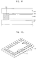
- FIG. 11 is a cross-sectional view illustrating a display device in accordance with Embodiment 7 of the present invention.
- FIG. 12A is a perspective view illustrating a method of manufacturing the display device shown in FIG. 11 ;
- FIGS. 12B to 12D are plan views illustrating a method of manufacturing the display device shown in FIG. 11 .
- first, second, third, etc. may be used herein to describe various elements, components, regions, layers and/or sections, these elements, components, regions, layers and/or sections should not be limited by these terms. These terms are only used to distinguish one element, component, region, layer or section from another region, layer or section. Thus, a first element, component, region, layer or section discussed below could be termed a second element, component, region, layer or section without departing from the teachings of the present invention.
- spatially relative terms such as “beneath,” “below,” “lower,” “above,” “upper” and the like, may be used herein for ease of description to describe one element or feature's relationship to another element(s) or feature(s) as illustrated in the figures. It will be understood that the spatially relative terms are intended to encompass different orientations of the device in use or operation in addition to the orientation depicted in the figures. For example, if the device in the figures is turned over, elements described as “below” or “beneath” other elements or features would then be oriented “above” the other elements or features. Thus, the exemplary term “below” can encompass both an orientation of above and below. The device may be otherwise oriented (rotated 90 degrees or at other orientations) and the spatially relative descriptors used herein interpreted accordingly.
- Example embodiments of the invention are described herein with reference to cross-sectional illustrations that are schematic illustrations of idealized example embodiments (and intermediate structures) of the present invention. As such, variations from the shapes of the illustrations as a result, for example, of manufacturing techniques and/or tolerances, are to be expected. Thus, example embodiments of the present invention should not be construed as limited to the particular shapes of regions illustrated herein but are to include deviations in shapes that result, for example, from manufacturing. For example, an implanted region illustrated as a rectangle will, typically, have rounded or curved features and/or a gradient of implant concentration at its edges rather than a binary change from implanted to non-implanted region.
- a buried region formed by implantation may result in some implantation in the region between the buried region and the surface through which the implantation takes place.
- the regions illustrated in the figures are schematic in nature and their shapes are not intended to illustrate the actual shape of a region of a device and are not intended to limit the scope of the present invention.
- FIG. 1 is a disassembled perspective view illustrating a display device in accordance with Embodiment 1 of the present invention
- FIG. 2 is a cross-sectional view taken along a line I-I′ shown in FIG. 1 .
- a display device 500 includes a first substrate 100 , a second substrate 200 , a sealant 300 , and a liquid crystal layer 400 .
- the first substrate 100 and the second substrate 200 may include a plurality of pixel regions Px.
- the first substrate 100 may be divided into a first display area DA 1 and a first peripheral area PA 1 surrounding the first display area DA 1 .
- the pixel regions Px of the first display area DA 1 may be defined by signal lines GL and DL formed on a first base substrate 110 .
- Each of the pixel regions Px in the first display area DA 1 may include a thin-film transistor (TFT) serving as a switching element, a pixel electrode 170 electrically connected to the TFT, and a storage capacitor (not shown).
- the signal lines GL and DL may include a gate line GL and a data line DL crossing each other.
- the TFT may include a gate electrode 120 connected to the gate line GL, a semiconductor pattern 140 formed on a gate insulating layer 130 which covers and overlaps the gate electrode 120 , a source electrode 152 overlapped with a portion of the semiconductor pattern 140 , and a drain electrode 154 overlapped with a portion of the semiconductor pattern 140 .
- the semiconductor pattern 140 may include a semiconductor layer 140 a and an ohmic contact layer 140 b .
- the source electrode 152 may be electrically connected to the data line DL.
- the pixel electrode 170 may be formed on a passivation layer 160 .
- the passivation layer 160 may cover the source electrode 152 and expose a portion of the drain electrode 154 .
- the pixel electrode 170 may electrically contact the drain electrode 154 to be connected to the TFT.
- the second substrate 200 may face the first substrate 100 .
- the second substrate 200 may be divided into a second display area DA 2 including a plurality of pixel regions Px and a second peripheral area PA 2 surrounding the second display area DA 2 .
- Each of the pixel regions Px in the second display area DA 2 may be defined by a black matrix pattern 220 which is formed on a second base substrate 210 .
- Each of the pixel regions Px in the second display area DA 2 may include a color filter 230 and a common electrode layer 250 .
- the black matrix pattern 220 may be formed on the second base substrate 210 corresponding to the gate line GL and data line DL of the first substrate 100 .
- the color filter 230 may be formed on the second base substrate 210 corresponding to the pixel electrode 170 of the first substrate 100 .
- the sealant 300 may be interposed between the first substrate 100 and the second substrate 200 .
- the sealant 300 may combine the first substrate 100 with the second substrate 200 .
- the sealant 300 may be disposed between the first peripheral area PA 1 and the second peripheral area PA 2 .
- the sealant may include a photocuring material and a thermosetting material.
- the photocuring material may be formed by hardening using multiphoton absorption, and the thermosetting material may be formed by hardening using heat.
- the photocuring material may be formed from a photosensitive compound including a photosensitive group and a photoinitiator.
- the photoinitiator may initiate a hardening reaction of the photosensitive compound.
- the photoinitiator may include an electron donor, an electron acceptor and a pi ( ⁇ ) bond.
- Examples of a material that may be used for the photosensitive compound may include ceramer, polydimethylsiloxane, Epon SU-8 (product, Shell Chemicals, Netherlands), SCR-701 (product, Japanese Rubber Co., Japan), etc.
- the photosensitive compound may include a net structure.
- the photosensitive compound may be formed by reacting a hydrogel or a silicate-based acrylate or epoxide.
- the hydrogel or the silicate-based acrylate or epoxide may be formed from acrylic resin, acryloyl acetone, acryl amide, etc.
- Examples of a material that may be used for the photoinitiator may include bis(2,4,6-trimethylbenzoyl)phenylphosphine oxide, 2-methoxy-1,2-diphenylethanone, 2,3-isopropylthoixanthone, diaryl iodonium, triaryl sulfonium salts, etc.
- the thermosetting material may be formed using a thermal sealing material including a thermal compound which includes a thermal sensitive group.
- the thermal sealing material may be hardened by heat to form the thermosetting material.
- Examples of a material that may be used for the thermal compound may include phenol resin, amino resin, epoxy resin, urea resin, unsaturated polyester resin, etc.
- the sealant 300 may include a first seal line 310 and a second seal line 320 which is formed along the first seal line 310 .
- the first seal line 310 may include the photocuring material hardened by the multiphoton absorption.
- the first seal line 310 may be formed on the first peripheral area PA 1 surrounding the first display area DA 1 .
- the first seal line 310 may be formed adjacent the liquid crystal layer 400 .
- the second seal line 320 may include the thermosetting material.
- the second seal line 320 may be formed along an edge portion of the first seal line 310 on the first peripheral area PA 1 .
- the second seal line 320 may contact the first seal line 310 .
- the second seal line 320 may be separated from the liquid crystal layer 400 by the first seal line 310 .
- the liquid crystal layer 400 may be interposed between the first and second substrates 100 and 200 .
- the liquid crystal layer 400 may include a plurality of liquid crystal molecules.
- An image is displayed on the LCD device 500 according to the light transmittance of the liquid crystal molecules, which varies according to a voltage applied thereto.
- FIGS. 3A , 3 B, 3 C and 3 D are perspective views illustrating a method of manufacturing the display device shown in FIG. 1 .
- FIG. 3A is a perspective view illustrating a step of coating the photosensitive sealing material and the thermal sealing material.
- the photosensitive sealing material is coated on the first peripheral area PA 1 of the first substrate 100 to form a first primary line 10 .
- the thermal sealing material is coated on the first peripheral area PA 1 along the first primary line 10 to form a second primary line 20 with the first primary line 10 .
- a dispersion device SFM may be disposed over the first peripheral area PA 1 of the first substrate 100 .
- the dispersion device SFM may provide the photosensitive sealing material and the thermal sealing material to the first substrate 100 .
- the dispersion device SFM may move along the first peripheral area PA 1 to form the first and second primary lines 10 and 20 .
- the first and second primary lines 10 and 20 may not be overlapped with each other.
- the photosensitive sealing material and the thermal sealing material which are coated on the first substrate 100 may not be mixed with each other.
- the dispersion device SFM may include a first syringe SYR 1 and a second syringe SYR 2 .
- the first syringe SYR 1 may disperse the photosensitive sealing material contained in the first syringe SYR 1 .
- FIG. 3B is a perspective view illustrating a step of hardening the photosensitive sealing material which is coated on the first substrate to form first seal line 310 .
- FIG. 4A illustrates the step of hardening the photosensitive sealing material shown in FIG. 3B
- FIG. 4B is a cross-sectional view illustrating a step of hardening the photosensitive sealing material shown in FIG. 3B .
- the photosensitive compound of the photosensitive sealing material is indicated as “A”, and the photoinitiator is indicated as “B”.
- the thermal compound of the thermal sealing material is indicated as “D”.
- the first primary line 10 may be hardened by the multiphoton absorption to form the first seal line 310 .
- the photosensitive sealing material may be hardened by the multiphoton absorption to form the photocuring material.
- the photosensitive compound “A” may include a main chain “a 1 ” and a photosensitive group “a 2 ” combined to the main chain “a 1 ”.
- the photosensitive group “a 2 ” may be an acryl group.
- the photoinitiator “B” may absorb the photochemical reaction energy (Ex) of pulse light which is generated by a pulse laser in one example.
- the photoinitiator “B” which absorbs the photochemical reaction energy (Ex) may attack the photosensitive group “a 2 ”.
- the photoinitiator “B” may be combined with the main chain “a 1 ” of the photosensitive compound “A” after the photoinitiator “B” initiates the hardening reaction.
- the photosensitive sealing material of the first primary line 10 may be hardened to form the first seal line 310 including the photocuring material.
- the pulse light having a pulse state may be irradiated along and over the first primary line 10 .
- the pulse light may be irradiated to the first primary line 10 using the pulse laser.
- the pulse laser may generate the pulse light of femtoseconds (10 ⁇ 15 seconds) or picoseconds (10 ⁇ 12 seconds).
- the energy level of the pulse light may be lower than the photochemical reaction energy (Ex) level of the photosensitive sealing material.
- the photochemical reaction energy (Ex) level may be a photochemical reaction energy level of the photoinitiator “B” of the photosensitive sealing material.
- the pulse laser may partially provide the pulse light to the first primary line 10 .
- the pulse light which is generated by the pulse laser may provide a 1/n energy level (Ex/n, “n” presents a natural number greater than or equal to 2) of the photochemical reaction energy (Ex) to the photoinitiator.
- the photoinitiator may absorb “n” photons from the pulse laser, and each of “n” photons may have the 1/n energy level (Ex/n).
- the photoinitiator “B” may substantially absorb the photochemical energy level (Ex) in total, despite receiving the 1/n energy level (Ex/n).
- the photochemical reaction energy (Ex) has a wavelength in a range of about 200 nm to about 400 nm
- the pulse light has a wavelength in a range of about 400 nm to about 1,200 nm.
- the photoinitiator “B” may absorb two photons, each having a wavelength of about 800 nm, and thus the photoinitiator “B” may substantially absorb about 400 nm in total.
- the photoinitiator “B” may absorb three photons each having a wavelength of about 600 nm, and thus the photoinitiator “B” may substantially absorb about 200 nm in total by the multiphoton absorption.
- the hardening reaction of the photosensitive sealing material may be initiated by a low energy, for example, the pulse light having a wavelength of visible light or infrared (IR) light to form the photocuring material.
- a low energy for example, the pulse light having a wavelength of visible light or infrared (IR) light to form the photocuring material.
- IR infrared
- circuits or materials formed on the first peripheral area PA 1 may be protected from change caused by a high energy level, for example, having the wavelength of ultraviolet (UV) light.
- UV ultraviolet
- the formation of a UV blocking mask which is expensive, may be omitted, and thus the productivity and manufacturing efficiencies of the display device may be improved.
- the thermal compound “D” of the thermal sealing material in the second primary line 20 may include a main chain “d 1 ” and the thermal group “d 2 ” combined to the main chain “d 1 ”.
- the thermal group “d 2 ” may be an epoxy group.
- the thermal sealing material and the thermal compound “D” of the second primary line 20 do not react.
- the first seal line 310 prevents the thermal compound “D” from flowing into the first display area DA 1 .
- FIG. 3C is a perspective view illustrating a step of dropping the liquid crystal composition.
- the liquid crystal composition 30 may be dropped on the first display area DA 1 .
- the liquid crystal composition 30 may be dotted on the first display area DA 1 . Because the liquid crystal composition 30 may be dropped on the first substrate 100 including the first seal line 310 , the liquid crystal composition 30 may not be mixed with the photosensitive sealing material.
- the photosensitive sealing material may be hardened to form the photocuring material before dropping the liquid crystal composition, and thus the liquid crystal composition 30 may be prevented from flowing into the first display area DA 1 .
- the photoinitiator may be entirely reacted by the pulse light, and thus the liquid crystal composition 30 may not be affected by the photoinitiator.
- first seal line 310 may be formed on the first substrate 100 before combining the first substrate 100 with the second substrate 200 , and thus the first seal line 310 may serve as a dam preventing material from inflowing into the first display area DA 1 .
- stains in the display device which may be generated by contamination of the liquid crystal composition 30 from the photosensitive sealing material and the thermal sealing material, may be prevented.
- FIG. 3D is a perspective view illustrating a step of arranging the first substrate to face the second substrate and a step of hardening the thermal sealing material.
- the second substrate 200 may face the first substrate 100 including a first seal line 310 , the second primary line 20 and the liquid crystal composition 30 dropped on the first substrate 100 .
- the first seal line 310 may serve as a spacer keeping a gap between the first and second substrates 100 and 200 .
- the gap may be substantially the same as the height of the first seal line 310 .
- the thermal sealing material may flow due to a pressure received between the first and second substrates 100 and 200 .
- the first seal line 310 prevents the thermal sealing material from flowing into the first display area DA 1 .
- the first and second substrates 100 and 200 may be heated by heat to harden the second primary line 20 .
- the thermal sealing material may be hardened by the heat to form the second seal line 320 including the thermosetting material.
- the second seal line 320 may substantially and physically combine the first substrate 100 with the second substrate 200 to manufacture the display device 500 ( FIGS. 1 and 2 ).
- a display device in accordance with another embodiment is substantially the same as the display device shown in FIGS. 1 and 2 . Thus, any repetitive description will be omitted.
- a method of manufacturing a display device in accordance with a second embodiment is substantially the same as the method shown in FIGS. 3A , 3 B, 3 C and 3 D, except for hardening a photosensitive sealing material. Thus, any repetitive description will be omitted.
- a photosensitive sealing material may be coated on the a first peripheral area PA 1 of a first substrate 100 to form a first primary line 10
- a thermal sealing material may be coated on the first peripheral area PA 1 to form a second primary line 20 .
- FIG. 5A illustrates a step of hardening a photosensitive sealing material in accordance with Embodiment 2
- FIG. 5B is a cross-sectional view illustrating a step of hardening a photosensitive sealing material in accordance with Embodiment 2 of the present invention.
- pulse light may irradiate the first primary line 10 including the photosensitive sealing material.
- the photosensitive sealing material may include a photosensitive compound “A”, a photoinitiator “B”, and a hybrid compound “E”.
- the photosensitive compound “A” may include a main chain “a 1 ” and a photosensitive group “a 2 ” combined with the main chain “a 1 ”.
- the photoinitiator “B” may absorb the photochemical reaction energy (Ex) of pulse light which is generated by a pulse laser.
- the photoinitiator “B” which absorbs the photochemical reaction energy (Ex) may attack the photosensitive group “a 2 ”.
- the photoinitiator “B” which absorbs the photochemical reaction energy (Ex) may attack the hybrid compound “E” to initiate a portion of the hardening reaction of the hybrid compound “E”.
- the hybrid compound “E” may include a main chain “e 1 ”, a photosensitive group “e 2 ” combined with the main chain “e 1 ”, and a thermal group “e 3 ” combined with the main chain “e 1 ”.
- the photosensitive group “e 2 ” may be substantially the same as the photosensitive group “a 2 ” of the photosensitive compound “A”.
- the photosensitive group “e 2 ” may be an acryl group.
- the photoinitiator “B” may attack the photosensitive group “a 2 ”, and the photoinitiator “B” may attack the photosensitive group “e 2 ”.
- the thermal group “e 3 ” may not be reacted by the pulse light, and thus the hybrid compound “E” may not be reacted by the pulse light.
- the thermal sealing material may also include the hybrid compound “E”.
- the photosensitive group “e 2 ” of the hybrid compound “E” may be reacted by the photoinitiator “B” which is reacted by the pulse light.
- a portion of the hybrid compound “E” may participate in the hardening reaction of the main chain “a 1 ” of the photosensitive compound “A”.
- the photosensitive compound “A” and a portion of the hybrid compound “E” may be hardened by the photoinitiator “B” to form the photocuring material.
- the first seal line 310 may be formed on the first peripheral area PA 1 .
- the second seal line 20 may include a thermal compound “D” of the thermal sealing material and the thermal group “e 3 ”.
- the thermal group “e 3 ” may be combined with an opposing portion of the hybrid compound “E” which is combined with the photocuring material.
- a second substrate 200 may be opposed to the first substrate 100 including the first seal line 310 , the second primary line 20 , and a liquid crystal composition which is dropped on the first substrate 100 .
- the first and second substrates 100 and 200 may be heated to form the second seal line 320 surrounding the first seal line 310 .
- the thermal compound “D” may be hardened by the heat, and the thermal group “e 3 ” of the hybrid compound “E” which is combined with the photocuring material may be hardened with the thermal compound “D”.
- the display device 500 shown in FIGS. 1 and 2 may be manufactured.
- the first seal line 310 which may serve as a dam and a spacer may be combined with the second seal line 320 by the hybrid compound “E”.
- adhesive strength between the sealant 300 including the first and second seal lines 310 and 320 and the first substrate 100 may be improved, and adhesive strength between the sealant 300 and the second substrate 200 may be improved.
- the first and second substrates 100 and 200 may be strongly combined with each other by the sealant 300 .
- a display device in accordance with another embodiment is substantially the same as the display device shown in FIGS. 1 and 2 . Thus, any repetitive description will be omitted.
- FIGS. 6A , 6 B and 6 C are perspective views illustrating a method of manufacturing a display device in accordance with Embodiment 3 of the present invention.
- a first primary line 10 may be formed on a first peripheral area PA 1 surrounding a first display area DA 1 of a first substrate 100 .
- a first syringe SYR 1 may disperse the photosensitive sealing material along the first peripheral area PA 1 to form the first primary line 10 .
- the photosensitive sealing material may include a photosensitive compound and a photoinitiator.
- pulse light may be provided to the first substrate 100 including the first primary line 10 to form a first seal line 310 .
- the energy level of the pulse light may be lower than the photochemical reaction energy (Ex) of the photosensitive sealing material.
- the photochemical reaction energy (Ex) may be a photochemical reaction energy level of the photoinitiator of the photosensitive sealing material.
- the pulse laser may partially provide the pulse light to the first primary line 10 .
- the photoinitiator may absorb a plurality of photons having an energy level of the pulse light, and thus the photoinitiator may absorb energy which substantially is the same as the energy level of the pulse light in total by the multiphoton absorption.
- the photosensitivity sealing material may be hardened to form the first seal line 310 .
- FIG. 6C is a perspective view illustrating a step of coating the thermal sealing material.
- a second primary line 20 may be formed on the first peripheral area PA 1 of the first substrate 100 along the first seal line 310 .
- a second syringe SYR 2 may disperse the thermal sealing material along the first peripheral area PA 1 to form the second primary line 20 .
- the second primary line 20 may be formed along an edge portion of the first seal line 310 to prevent the thermal sealing material from flowing into the first display area DA 1 .
- a second substrate 200 may face the first substrate 100 including the second primary line 20 .
- the second substrate 200 may uniformly be spaced apart from the first substrate 100 by the first seal line 310 .
- the first and second substrates 100 and 200 may be heated to harden the second primary line 20 , and thus a second seal line 320 may be formed.
- the first and second substrates 100 and 200 may be combined by a sealant 300 including the first and second seal lines 310 and 320 , and the display device 500 shown in FIG. 1 may be manufactured.
- a display device in accordance with another embodiment is substantially the same as the display device shown in FIGS. 1 and 2 . Thus, any repetitive description will be omitted.
- a method of manufacturing a display device in accordance with an embodiment is substantially the same as the method shown illustrated in Embodiment 3, except for coating a photosensitive composition and hardening the photosensitive sealing material. Thus, any repetitive description will be omitted.
- FIG. 7 is a perspective view illustrating steps of coating and hardening a photosensitive sealing material in accordance with Embodiment 4 of the present invention.
- a first seal line 310 may be formed on a first peripheral area PA 1 surrounding a first display area DA 1 of a first substrate 100 .
- a first syringe SYR 1 containing a photosensitive sealing material may disperse the photosensitive sealing material.
- the photosensitive sealing material which is dispersed on the first peripheral area PA 1 may receive pulse light from a light-providing portion LD connected to the first syringe SYR 1 .
- the photosensitive sealing material may be hardened by the pulse light to form a first seal line 310 .
- the first syringe SYR 1 may disperse the photosensitive composition to form a first primary line 10 , and the light-providing portion LD may move along the first primary line 10 to provide the pulse light to the first primary line 10 .
- the pulse light may be provided to the first primary line 10 immediately after the first primary line 10 may be formed by the first syringe SYR 1 .
- a final point of the first primary 10 may meet a starting edge point of the first seal line 310 .
- the final point may be a point that the photosensitive sealing material is not coated any longer in the process of coating the photosensitive sealing material.
- the starting point of the first seal line 310 may be a point that the pulse light may initially be provided to the first primary line 10 in the process of providing the pulse light.
- the pulse light may be provided to the final point after meeting the final portion of the first primary line 10 and the starting point of the first seal line 310 , and thus a step of forming the first seal line 310 may be completed.
- a second substrate 200 may face the first substrate 100 including a second primary line 20 , the first seal line 310 , and a dropped liquid crystal composition 30 .
- the first and second substrates 100 and 200 may be heated to harden the second primary line 20 , and thus a second seal line 320 may be formed along the first seal line 310 .
- the first and second substrates 100 and 200 may be combined by a sealant 300 including the first and second seal lines 310 and 320 , and the display device 500 shown in FIG. 1 may be manufactured.
- the first seal line 310 may be formed using the first syringe SYR 1 and the light-providing portion LD which are combined with each other and the first seal line 310 may be formed by partially providing the pulse light to the first primary line 10 .
- the process of forming the first seal line 310 may be simplified.
- a display device in accordance with another embodiment is substantially the same as the display device shown in FIGS. 1 and 2 . Thus, any repetitive description will be omitted.
- a method of manufacturing a display device in accordance with an embodiment is substantially the same as the method shown illustrated in Embodiment 1, except for coating a photosensitive composition and hardening the photosensitive sealing material. Thus, any repetitive description will be omitted.
- FIG. 8 is a plan view illustrating a step of coating a photosensitive sealing material and a thermal sealing material and a step of hardening the photosensitive sealing material.
- a photosensitive sealing material and a thermal sealing material may be simultaneously coated on a first peripheral area PA 1 surrounding a first display area DA 1 of a first substrate 100 .
- a first primary line 10 and a second primary line 20 may be simultaneously formed on the first peripheral area PA 1 , and pulse light may be provided to the first primary line 10 to form a first seal line 310 .
- a first injection nozzle 1 may inject the photosensitive sealing material on the first peripheral area PA 1 to form the first primary line 10 .
- a second injection nozzle 2 may inject the thermal sealing material on the first peripheral area PA 1 to form the second primary line 20 .
- the first and second primary lines 10 and 20 may be simultaneously formed.
- Pulse light may be provided to the first primary line 10 by a light-providing portion 3 disposed adjacent to the first injection nozzle 1 .
- the photosensitive sealing material may be hardened by the pulse light to form the first seal line 310 .
- a second substrate 200 may face the first substrate 100 including the first seal line 310 , the second primary line 20 , and a dropped liquid crystal composition 30 .
- the first and second substrates 100 and 200 may be heated to harden the second primary line 20 , and thus a second seal line 320 may be formed along the first seal line 310 .
- the first and second substrates 100 and 200 may be combined by a sealant 300 including the first and second seal lines 310 and 320 , and the display device 500 shown in FIGS. 1 and 2 may be manufactured.
- the first and second primary lines 10 and 20 may be simultaneously formed by using the dispersion device including the first injection nozzle 1 , the second injection nozzle 2 , and the light-providing portion 3 .
- the pulse light may be partially provided to the first primary line 10 to be simplified.
- a delay between forming the first primary line 10 and forming the second primary line 20 may be minimized, and thus the thermal sealing material of the second primary line 20 may be easily prevented from flowing into the first display area DA 1 .
- FIG. 9 is a cross-sectional view illustrating a display device in accordance with Embodiment 6 of the present invention.
- a display device in accordance with an embodiment is substantially the same as the display device shown in FIG. 1 , except for a first seal line 310 , a second seal line 320 , and a mixing portion 330 . Thus, any repetitive description will be omitted.
- the display device includes a first substrate 100 , a second substrate 200 , a sealant 300 , and a liquid crystal layer 400 .
- the first substrate 100 may include an array layer 100 A which is formed on a first base substrate 110 .
- the array layer 100 A may include a gate line GL, a data line DL, a TFT, and a pixel electrode 170 .
- the second substrate 200 may include a color layer 200 A which is formed on a second base substrate 210 .
- the color layer 200 A may include a black matrix pattern 220 , a color filter 230 , and a common electrode layer 250 .
- the sealant 300 may include a first seal line 310 , a second seal line 320 , and a mixing portion 330 .
- the first seal line 310 may include a photocuring material
- the second seal line 320 may include a thermosetting material
- the mixing portion 330 may include the photocuring material and the thermosetting material.
- the photocuring material of the first seal line 310 may be formed by hardening a photosensitive sealing material using multiphoton absorption.
- the thermosetting material of the second seal line 320 may be formed by hardening a thermal sealing material.
- the first seal line 310 may surround an edge portion of the liquid crystal layer 400 and directly contact a liquid crystal composition 30 of the liquid crystal layer 400 .
- the mixing portion 330 is mixed with the photocuring material and the thermosetting material.
- the photosensitive sealing material may be hardened by the multiphoton absorption and the thermal sealing material may be hardened by heat.
- the sealant 300 including the mixing portion 330 may be strongly combined with the first substrate 100 and the second substrate 200 .
- FIGS. 10A and 10B are perspective views illustrating a method of manufacturing the display device shown in FIG. 9 .
- the photosensitive sealing material may be coated on the first peripheral area PA 1 to form a first primary line 10 .
- the first primary line 10 may surround the display area DA 1 and be formed on the first peripheral area PA 1 .
- the photosensitive sealing material may include a photosensitive compound and a photoinitiator.
- the thermal sealing material may be coated on the first peripheral area PA 1 including the first primary line 10 to form a second primary line 20 and a primary mixing portion 40 .
- the second primary line 20 may be formed along the first primary line 10 on the first peripheral area PA 1 .
- the primary mixing portion 40 may be formed on an area overlapping the second primary line 20 with the first primary line 10 while the second primary line 20 is formed on the area.
- the photosensitive sealing material of the first primary line 10 may be mixed with the thermal sealing material of the second primary line 20 to form the primary mixing portion 40 .
- Pulse light may be partially provided to the first primary line 10 and the primary mixing portion 40 of the first substrate 100 including the first and second primary lines 10 and 20 and the primary mixing portion 40 , and thus the first seal line 310 and a partial-mixing portion (not shown) may be formed.
- the first seal line 310 may include the photocuring material which is formed by hardening the photosensitive sealing material.
- the partial-mixing portion may include the photocuring material and the thermal sealing material.
- a second substrate 200 may face the first substrate 100 including the first seal line 310 , the partial-mixing portion, the second primary line 20 , and a dropped liquid crystal composition 30 .
- the first and second substrates 100 and 200 may be heated to harden the second primary line 20 and the partial-mixing portion, and thus the second seal line 320 and the mixing portion 320 may be formed.
- the second seal line 320 may include the thermosetting material and the mixing portion 330 may include the photocuring material and the thermosetting material.
- the sealant 300 including the mixing portion 330 may be strongly combined with the first substrate 100 and the second substrate 200 .
- FIG. 11 is a cross-sectional view illustrating a display device in accordance with Embodiment 7 of the present invention.
- a display device in accordance with an embodiment is substantially the same as the display device shown in FIG. 1 , except for a sealant 300 . Thus, any repetitive description will be omitted.
- the display device includes a first substrate 100 , a second substrate 200 , a sealant 300 , and a liquid crystal layer 400 .
- the first substrate 100 may include an array layer 100 A which is formed on a first base substrate 110 .
- the array layer 100 A may include a gate line GL, a data line DL, a TFT, and a pixel electrode 170 .
- the second substrate 200 may include a color layer 200 A which is formed on a second base substrate 210 .
- the color layer 200 A may include a black matrix pattern 220 , a color filter 230 , and a common electrode layer 250 .
- the sealant 300 may be formed on a first peripheral area PA 1 surrounding a display area DA 1 which is formed on the array layer 100 A.
- the sealant 300 may include a photocuring material and a thermosetting material.
- the photocuring material and the thermosetting material which are mixed with each other may define the sealant 300 .
- the photocuring material may be formed by hardening a photosensitive sealing material using multiphoton absorption.
- the thermosetting material may be formed by hardening a thermal sealing material. A portion of the sealant 300 may be hardened by multiphoton absorption and a remaining portion of the sealant 300 may be hardened by heat, and thus the sealant 300 may be formed.
- contamination of the liquid crystal layer 400 may be prevented from a photoinitiator in the photosensitive sealing material, because the photosensitive sealant may be hardened before dropping a liquid crystal composition of the liquid crystal layer 400 .
- the photocuring material is formed from the photosensitive sealing material which receives pulse light having a lower energy level than a photochemical energy level of the photosensitive sealing material, and thus alteration of the circuits or materials formed on the display area and the peripheral area may be prevented by hardening the sealant. Additionally, the formation of the UV blocking mask, which is expensive, may be omitted, and thus the productivity of the display device may be improved.
- FIG. 12A is a perspective view illustrating a method of manufacturing the display device shown in FIG. 11
- FIGS. 12B , 12 C and 12 D are views illustrating a method of manufacturing the display device shown in FIG. 11 .
- a mixing composition including the photosensitive sealing material and the thermal sealing material may be coated on the first peripheral area PA 1 of the first substrate 100 to form a third primary line 50 .
- At least one of the photosensitive sealing material and the thermal sealing material may further include a hybrid compound, and thus the mixing composition may include the hybrid compound.
- the third primary line 50 may be formed on the first peripheral area PA 1 surrounding the first display area DA 1 .
- the photosensitive sealing material, thermal sealing material, and the hybrid compound may randomly be distributed on the first peripheral area PA 1 .
- FIG. 12B is a conceptual view of an enlarged “F” part of the third primary line shown in FIG. 12A .
- the third primary line 50 may include a photosensitive compound “A” and a photoinitiator “B of the photosensitive sealing material, a thermal compound “B” of the thermal sealing material, and the hybrid compound “E” which are randomly distributed to each other.
- the photosensitive compound “A” may include a photosensitive group.
- the photosensitive compound “A” may be hardened by the photoinitiator “B”.
- the photoinitiator “B” may absorb a photochemical reaction energy using multiphoton absorption.
- the hybrid compound “E” may include the photosensitive group of the photosensitive compound “A” and the thermal group of the thermal compound “D”.
- pulse light may be provided to the third primary line 50 , and thus the photosensitive compound “A”, the photoinitiator “B”, and the hybrid compound “E” may react to form a partial-mixing portion 52 .
- the photoinitiator “B” may absorb multiphotons by the pulse light to be initiated to a hardening reaction of the photosensitive group in the photosensitive compound “A” and the hybrid compound “E”.
- the photosensitive compound “A” may be reacted with the photoinitiator “B”.
- the photosensitive compound “A” which is reacted with the photoinitiator “B” may be combined with an edge portion of the hybrid compound “E”.
- the edge portion of the hybrid compound “E” may be a portion including the photosensitive group.
- the partial-mixing portion 52 may include the photocuring material formed by combining the photosensitive compound “A” and the photoinitiator “B”.
- a liquid crystal composition may be dropped on the first display area DA 1 of the first substrate 100 including the partial-mixing portion 52 .
- the partial-mixing portion 52 may not include a residual photoinitiator “B” and the photosensitive sealing material may be entirely hardened, and thus contamination of the liquid crystal composition may be prevented from the photoinitiator “B” or the photosensitive group.
- a second substrate 200 may face the first substrate 100 including the partial-mixing portion 52 and a dropped liquid crystal composition.
- the first and second substrates 100 and 200 may be heated to harden the thermal compound “D”, and thus the thermosetting material may be formed.
- thermosetting material may be formed by combining the thermal compounds “D” with each other or combining the thermal compound “D” with the thermal group which is an opposing edge portion of the hybrid compound “E”.
- the thermosetting material may be formed to form the sealant 300 including the photocuring material and the thermosetting material.
- the sealant 300 may be strongly combined with the first substrate 100 and the second substrate 200 by the hybrid compound “E”.
- a liquid crystal composition may be dropped on the second substrate.
- a first substrate including an array layer may face the second substrate including a photocuring material, a thermal sealing material, and a dropped liquid crystal composition, and thus the thermal sealing material may be hardened to a thermosetting material.
- the first and second substrates may be combined by a sealant including the photocuring material and the thermosetting material.
- contamination of the liquid crystal composition may be prevented from the sealant, and thus generating stains in the display device may be prevented.
- the reliability of manufacturing the display device may be improved and the display quality may be improved.
- the photocuring material is formed from the photosensitive sealing material which receives pulse light having a lower energy level than a photochemical energy level of the photosensitive sealing material, and thus alteration of the circuits or materials formed on the display area and the peripheral area may be prevented by hardening the sealant. Formation of the UV blocking mask, which is expensive, may be omitted, and thus the productivity of the display device may be improved.
- the seal line including the photocuring material may serve as the dam of the liquid crystal composition and as the cell gap spacer of the first and second substrates.
- the margin of dropping the liquid crystal composition may be improved.
Landscapes
- Physics & Mathematics (AREA)
- Nonlinear Science (AREA)
- Chemical & Material Sciences (AREA)
- Crystallography & Structural Chemistry (AREA)
- General Physics & Mathematics (AREA)
- Optics & Photonics (AREA)
- Mathematical Physics (AREA)
- Liquid Crystal (AREA)
Abstract
Description
Claims (22)
Applications Claiming Priority (3)
| Application Number | Priority Date | Filing Date | Title |
|---|---|---|---|
| KR1020080106532A KR101495214B1 (en) | 2008-10-29 | 2008-10-29 | Display device and method of manufacturing the same |
| KR10-2008-0106532 | 2008-10-29 | ||
| KR2008-106532 | 2008-10-29 |
Publications (2)
| Publication Number | Publication Date |
|---|---|
| US20100103362A1 US20100103362A1 (en) | 2010-04-29 |
| US8089601B2 true US8089601B2 (en) | 2012-01-03 |
Family
ID=42117138
Family Applications (1)
| Application Number | Title | Priority Date | Filing Date |
|---|---|---|---|
| US12/419,954 Active 2030-02-18 US8089601B2 (en) | 2008-10-29 | 2009-04-07 | Display device and method of manufacturing the same |
Country Status (2)
| Country | Link |
|---|---|
| US (1) | US8089601B2 (en) |
| KR (1) | KR101495214B1 (en) |
Families Citing this family (11)
| Publication number | Priority date | Publication date | Assignee | Title |
|---|---|---|---|---|
| US20120044445A1 (en) * | 2010-08-17 | 2012-02-23 | Semiconductor Energy Laboratory Co., Ltd. | Liquid Crystal Device and Manufacturing Method Thereof |
| US8625067B2 (en) * | 2011-11-23 | 2014-01-07 | Shenzhen China Star Optoelectronics Technology Co., Ltd. | Sealant applying apparatus and sealant applying method for LCD substrate |
| US9625764B2 (en) * | 2012-08-28 | 2017-04-18 | Semiconductor Energy Laboratory Co., Ltd. | Display device and electronic device |
| JP2014071438A (en) * | 2012-10-02 | 2014-04-21 | Japan Display Inc | Liquid crystal display device |
| CN104956429B (en) * | 2013-01-30 | 2017-10-03 | 夏普株式会社 | Display device |
| KR20150038950A (en) * | 2013-10-01 | 2015-04-09 | 삼성디스플레이 주식회사 | Liquid crystal display and method of manufacturing the same |
| CN103785596A (en) * | 2014-01-20 | 2014-05-14 | 北京京东方光电科技有限公司 | Method and device for coating of frame sealing adhesives, and display device |
| JP5936747B2 (en) * | 2015-05-19 | 2016-06-22 | 芝浦メカトロニクス株式会社 | Manufacturing apparatus and manufacturing method for members constituting display device |
| CN105446022B (en) * | 2016-01-05 | 2019-08-06 | 京东方科技集团股份有限公司 | A kind of display panel and preparation method thereof, application |
| CN105759511A (en) * | 2016-04-15 | 2016-07-13 | 京东方科技集团股份有限公司 | Display panel and manufacturing method thereof, and display device and manufacturing method thereof |
| KR20190021467A (en) * | 2016-07-08 | 2019-03-05 | 헨켈 아게 운트 코. 카게아아 | A method of manufacturing a liquid crystal display and a curable resin composition used in the method |
Citations (7)
| Publication number | Priority date | Publication date | Assignee | Title |
|---|---|---|---|---|
| US20030137630A1 (en) * | 2002-01-24 | 2003-07-24 | Hirotaka Niiya | Display element and production method therefor |
| US20050231679A1 (en) * | 2002-01-28 | 2005-10-20 | Kyoritsu Chemical & Co., Ltd. | Sealing agent for LC dropping method for LCD panels |
| US7006193B2 (en) | 1999-05-10 | 2006-02-28 | Au Optronics Corporation | Method of sealing two substrates with a non-epoxy or epoxy-acrylate sealant using laser radiation |
| KR20070046421A (en) | 2005-10-31 | 2007-05-03 | 삼성전자주식회사 | Liquid crystal display panel and method of manufacturing the same |
| JP2008116825A (en) | 2006-11-07 | 2008-05-22 | Sekisui Chem Co Ltd | Sealing agent for liquid crystal display element, vertical conducting material and liquid crystal display element |
| US20080151172A1 (en) * | 2005-03-18 | 2008-06-26 | Sharp Kabushiki Kaisha | Liquid Crystal Panel and Method For Manufacturing the Same |
| US20080309866A1 (en) * | 2007-06-12 | 2008-12-18 | Au Optronics Corporation | Display Panel with Photo-Curable Sealant and Manufacture Method Thereof |
Family Cites Families (1)
| Publication number | Priority date | Publication date | Assignee | Title |
|---|---|---|---|---|
| KR20070035234A (en) * | 2005-09-27 | 2007-03-30 | 삼성전자주식회사 | Method and apparatus for manufacturing display substrate |
-
2008
- 2008-10-29 KR KR1020080106532A patent/KR101495214B1/en active IP Right Grant
-
2009
- 2009-04-07 US US12/419,954 patent/US8089601B2/en active Active
Patent Citations (8)
| Publication number | Priority date | Publication date | Assignee | Title |
|---|---|---|---|---|
| US7006193B2 (en) | 1999-05-10 | 2006-02-28 | Au Optronics Corporation | Method of sealing two substrates with a non-epoxy or epoxy-acrylate sealant using laser radiation |
| US20030137630A1 (en) * | 2002-01-24 | 2003-07-24 | Hirotaka Niiya | Display element and production method therefor |
| US6831725B2 (en) * | 2002-01-24 | 2004-12-14 | Sharp Kabushiki Kaisha | Display element having a seal member with UV curable and thermosetting resin layers and production method thereof |
| US20050231679A1 (en) * | 2002-01-28 | 2005-10-20 | Kyoritsu Chemical & Co., Ltd. | Sealing agent for LC dropping method for LCD panels |
| US20080151172A1 (en) * | 2005-03-18 | 2008-06-26 | Sharp Kabushiki Kaisha | Liquid Crystal Panel and Method For Manufacturing the Same |
| KR20070046421A (en) | 2005-10-31 | 2007-05-03 | 삼성전자주식회사 | Liquid crystal display panel and method of manufacturing the same |
| JP2008116825A (en) | 2006-11-07 | 2008-05-22 | Sekisui Chem Co Ltd | Sealing agent for liquid crystal display element, vertical conducting material and liquid crystal display element |
| US20080309866A1 (en) * | 2007-06-12 | 2008-12-18 | Au Optronics Corporation | Display Panel with Photo-Curable Sealant and Manufacture Method Thereof |
Also Published As
| Publication number | Publication date |
|---|---|
| US20100103362A1 (en) | 2010-04-29 |
| KR20100047576A (en) | 2010-05-10 |
| KR101495214B1 (en) | 2015-03-03 |
Similar Documents
| Publication | Publication Date | Title |
|---|---|---|
| US8089601B2 (en) | Display device and method of manufacturing the same | |
| CN104122729B (en) | Transparent display device and method of manufacturing the same | |
| US7598103B2 (en) | Liquid crystal display panel with different substrate materials and method of making the liquid crystal display panel | |
| KR101701977B1 (en) | Liquid crystal display device | |
| US20070095468A1 (en) | Sealant dispensing apparatus, liquid crystal display panel manufactured using the same and method of manufacturing liquid crystal display panel | |
| JP2007304273A (en) | Liquid crystal display element | |
| US9151998B2 (en) | Liquid crystal display and method of manufacturing the same | |
| JP5285809B2 (en) | Display device and manufacturing method thereof | |
| CN101080664A (en) | Panel and method for manufacturing same | |
| US20110134372A1 (en) | Polymer-dispersed liquid crystal display device and method of manufacturing the same | |
| KR20080082164A (en) | Liquid crystal display and method for manufacturing the same | |
| TWI422934B (en) | Liquid crystal display device and manufacturing method thereof | |
| US20160109748A1 (en) | Light-shielding mask and method of fabricating liquid crystal display device by using the same | |
| JP2007226223A (en) | Method of manufacturing liquid crystal display device | |
| JP2008139555A (en) | Liquid crystal display device and its manufacturing method | |
| JP2007193003A (en) | Display device | |
| KR100672641B1 (en) | Liquid Crystal Display Device and Method of manufacturing the same | |
| US9796050B2 (en) | Method for manufacturing display panel and display panel manufactured by the method | |
| US20100177417A1 (en) | Color filter substrate and method of manufacturing the same | |
| US20190310500A1 (en) | Display panel, collective display panel, and method of manufacturing display panel | |
| JP2007304274A (en) | Liquid crystal display element and manufacturing method | |
| KR20070070403A (en) | Liquid crystal display device and the fabrication method thereof | |
| JP2004325525A (en) | Substrate for liquid crystal display device, method of manufacturing substrate for liquid crystal display device, liquid crystal display device and method of manufacturing liquid crystal display device | |
| US20080212220A1 (en) | Color filter substrate and method for manufacturing the same | |
| TW591293B (en) | Liquid crystal display device |
Legal Events
| Date | Code | Title | Description |
|---|---|---|---|
| AS | Assignment |
Owner name: SAMSUNG ELECTRONICS CO., LTD.,KOREA, REPUBLIC OF Free format text: ASSIGNMENT OF ASSIGNORS INTEREST;ASSIGNORS:BYUN, HO-YUN;LEE, JUNG-HUN;JUNG, JI-YOON;AND OTHERS;REEL/FRAME:022517/0469 Effective date: 20090305 Owner name: SAMSUNG ELECTRONICS CO., LTD., KOREA, REPUBLIC OF Free format text: ASSIGNMENT OF ASSIGNORS INTEREST;ASSIGNORS:BYUN, HO-YUN;LEE, JUNG-HUN;JUNG, JI-YOON;AND OTHERS;REEL/FRAME:022517/0469 Effective date: 20090305 |
|
| FEPP | Fee payment procedure |
Free format text: PAYOR NUMBER ASSIGNED (ORIGINAL EVENT CODE: ASPN); ENTITY STATUS OF PATENT OWNER: LARGE ENTITY |
|
| STCF | Information on status: patent grant |
Free format text: PATENTED CASE |
|
| AS | Assignment |
Owner name: SAMSUNG DISPLAY CO., LTD., KOREA, REPUBLIC OF Free format text: ASSIGNMENT OF ASSIGNORS INTEREST;ASSIGNOR:SAMSUNG ELECTRONICS CO., LTD.;REEL/FRAME:029008/0744 Effective date: 20120904 |
|
| FPAY | Fee payment |
Year of fee payment: 4 |
|
| MAFP | Maintenance fee payment |
Free format text: PAYMENT OF MAINTENANCE FEE, 8TH YEAR, LARGE ENTITY (ORIGINAL EVENT CODE: M1552); ENTITY STATUS OF PATENT OWNER: LARGE ENTITY Year of fee payment: 8 |
|
| MAFP | Maintenance fee payment |
Free format text: PAYMENT OF MAINTENANCE FEE, 12TH YEAR, LARGE ENTITY (ORIGINAL EVENT CODE: M1553); ENTITY STATUS OF PATENT OWNER: LARGE ENTITY Year of fee payment: 12 |