US8089426B2 - Plasma display panel drive method of determining a subfield, having a low luminance, for performing an every-cell initialization operation and setting a width of a sustain pulse of the subfield for performing the every-cell initialization operation - Google Patents
Plasma display panel drive method of determining a subfield, having a low luminance, for performing an every-cell initialization operation and setting a width of a sustain pulse of the subfield for performing the every-cell initialization operation Download PDFInfo
- Publication number
- US8089426B2 US8089426B2 US11/628,434 US62843406A US8089426B2 US 8089426 B2 US8089426 B2 US 8089426B2 US 62843406 A US62843406 A US 62843406A US 8089426 B2 US8089426 B2 US 8089426B2
- Authority
- US
- United States
- Prior art keywords
- width
- sustain
- sustain pulse
- subfield
- discharge
- Prior art date
- Legal status (The legal status is an assumption and is not a legal conclusion. Google has not performed a legal analysis and makes no representation as to the accuracy of the status listed.)
- Expired - Fee Related, expires
Links
- 238000000034 method Methods 0.000 title claims description 30
- 238000006243 chemical reaction Methods 0.000 description 15
- 238000010586 diagram Methods 0.000 description 10
- 230000007423 decrease Effects 0.000 description 8
- 239000000758 substrate Substances 0.000 description 8
- 230000001174 ascending effect Effects 0.000 description 5
- 238000001514 detection method Methods 0.000 description 5
- 238000005192 partition Methods 0.000 description 4
- 230000000593 degrading effect Effects 0.000 description 3
- 230000003111 delayed effect Effects 0.000 description 3
- 239000012212 insulator Substances 0.000 description 3
- 230000002459 sustained effect Effects 0.000 description 3
- 229910052724 xenon Inorganic materials 0.000 description 3
- FHNFHKCVQCLJFQ-UHFFFAOYSA-N xenon atom Chemical compound [Xe] FHNFHKCVQCLJFQ-UHFFFAOYSA-N 0.000 description 3
- 101000631760 Homo sapiens Sodium channel protein type 1 subunit alpha Proteins 0.000 description 2
- 101000920618 Homo sapiens Transcription and mRNA export factor ENY2 Proteins 0.000 description 2
- 102100028910 Sodium channel protein type 1 subunit alpha Human genes 0.000 description 2
- 102100031954 Transcription and mRNA export factor ENY2 Human genes 0.000 description 2
- 230000015572 biosynthetic process Effects 0.000 description 2
- 230000003247 decreasing effect Effects 0.000 description 2
- 239000011521 glass Substances 0.000 description 2
- CPLXHLVBOLITMK-UHFFFAOYSA-N magnesium oxide Inorganic materials [Mg]=O CPLXHLVBOLITMK-UHFFFAOYSA-N 0.000 description 2
- 239000000395 magnesium oxide Substances 0.000 description 2
- AXZKOIWUVFPNLO-UHFFFAOYSA-N magnesium;oxygen(2-) Chemical compound [O-2].[Mg+2] AXZKOIWUVFPNLO-UHFFFAOYSA-N 0.000 description 2
- 230000037452 priming Effects 0.000 description 2
- 229910052782 aluminium Inorganic materials 0.000 description 1
- XAGFODPZIPBFFR-UHFFFAOYSA-N aluminium Chemical compound [Al] XAGFODPZIPBFFR-UHFFFAOYSA-N 0.000 description 1
- 239000003795 chemical substances by application Substances 0.000 description 1
- 239000003086 colorant Substances 0.000 description 1
- 238000005516 engineering process Methods 0.000 description 1
- 238000005286 illumination Methods 0.000 description 1
- 230000000977 initiatory effect Effects 0.000 description 1
- 239000000463 material Substances 0.000 description 1
- 229910052751 metal Inorganic materials 0.000 description 1
- 239000002184 metal Substances 0.000 description 1
- 239000000203 mixture Substances 0.000 description 1
- 229910052754 neon Inorganic materials 0.000 description 1
- GKAOGPIIYCISHV-UHFFFAOYSA-N neon atom Chemical compound [Ne] GKAOGPIIYCISHV-UHFFFAOYSA-N 0.000 description 1
- 239000002245 particle Substances 0.000 description 1
- 238000004544 sputter deposition Methods 0.000 description 1
- 239000010409 thin film Substances 0.000 description 1
- 239000002699 waste material Substances 0.000 description 1
Images


Classifications
-
- G—PHYSICS
- G09—EDUCATION; CRYPTOGRAPHY; DISPLAY; ADVERTISING; SEALS
- G09G—ARRANGEMENTS OR CIRCUITS FOR CONTROL OF INDICATING DEVICES USING STATIC MEANS TO PRESENT VARIABLE INFORMATION
- G09G3/00—Control arrangements or circuits, of interest only in connection with visual indicators other than cathode-ray tubes
- G09G3/20—Control arrangements or circuits, of interest only in connection with visual indicators other than cathode-ray tubes for presentation of an assembly of a number of characters, e.g. a page, by composing the assembly by combination of individual elements arranged in a matrix no fixed position being assigned to or needed to be assigned to the individual characters or partial characters
- G09G3/22—Control arrangements or circuits, of interest only in connection with visual indicators other than cathode-ray tubes for presentation of an assembly of a number of characters, e.g. a page, by composing the assembly by combination of individual elements arranged in a matrix no fixed position being assigned to or needed to be assigned to the individual characters or partial characters using controlled light sources
- G09G3/28—Control arrangements or circuits, of interest only in connection with visual indicators other than cathode-ray tubes for presentation of an assembly of a number of characters, e.g. a page, by composing the assembly by combination of individual elements arranged in a matrix no fixed position being assigned to or needed to be assigned to the individual characters or partial characters using controlled light sources using luminous gas-discharge panels, e.g. plasma panels
- G09G3/288—Control arrangements or circuits, of interest only in connection with visual indicators other than cathode-ray tubes for presentation of an assembly of a number of characters, e.g. a page, by composing the assembly by combination of individual elements arranged in a matrix no fixed position being assigned to or needed to be assigned to the individual characters or partial characters using controlled light sources using luminous gas-discharge panels, e.g. plasma panels using AC panels
- G09G3/291—Control arrangements or circuits, of interest only in connection with visual indicators other than cathode-ray tubes for presentation of an assembly of a number of characters, e.g. a page, by composing the assembly by combination of individual elements arranged in a matrix no fixed position being assigned to or needed to be assigned to the individual characters or partial characters using controlled light sources using luminous gas-discharge panels, e.g. plasma panels using AC panels controlling the gas discharge to control a cell condition, e.g. by means of specific pulse shapes
- G09G3/292—Control arrangements or circuits, of interest only in connection with visual indicators other than cathode-ray tubes for presentation of an assembly of a number of characters, e.g. a page, by composing the assembly by combination of individual elements arranged in a matrix no fixed position being assigned to or needed to be assigned to the individual characters or partial characters using controlled light sources using luminous gas-discharge panels, e.g. plasma panels using AC panels controlling the gas discharge to control a cell condition, e.g. by means of specific pulse shapes for reset discharge, priming discharge or erase discharge occurring in a phase other than addressing
- G09G3/2927—Details of initialising
-
- G—PHYSICS
- G09—EDUCATION; CRYPTOGRAPHY; DISPLAY; ADVERTISING; SEALS
- G09G—ARRANGEMENTS OR CIRCUITS FOR CONTROL OF INDICATING DEVICES USING STATIC MEANS TO PRESENT VARIABLE INFORMATION
- G09G3/00—Control arrangements or circuits, of interest only in connection with visual indicators other than cathode-ray tubes
- G09G3/20—Control arrangements or circuits, of interest only in connection with visual indicators other than cathode-ray tubes for presentation of an assembly of a number of characters, e.g. a page, by composing the assembly by combination of individual elements arranged in a matrix no fixed position being assigned to or needed to be assigned to the individual characters or partial characters
- G09G3/22—Control arrangements or circuits, of interest only in connection with visual indicators other than cathode-ray tubes for presentation of an assembly of a number of characters, e.g. a page, by composing the assembly by combination of individual elements arranged in a matrix no fixed position being assigned to or needed to be assigned to the individual characters or partial characters using controlled light sources
- G09G3/28—Control arrangements or circuits, of interest only in connection with visual indicators other than cathode-ray tubes for presentation of an assembly of a number of characters, e.g. a page, by composing the assembly by combination of individual elements arranged in a matrix no fixed position being assigned to or needed to be assigned to the individual characters or partial characters using controlled light sources using luminous gas-discharge panels, e.g. plasma panels
- G09G3/288—Control arrangements or circuits, of interest only in connection with visual indicators other than cathode-ray tubes for presentation of an assembly of a number of characters, e.g. a page, by composing the assembly by combination of individual elements arranged in a matrix no fixed position being assigned to or needed to be assigned to the individual characters or partial characters using controlled light sources using luminous gas-discharge panels, e.g. plasma panels using AC panels
- G09G3/291—Control arrangements or circuits, of interest only in connection with visual indicators other than cathode-ray tubes for presentation of an assembly of a number of characters, e.g. a page, by composing the assembly by combination of individual elements arranged in a matrix no fixed position being assigned to or needed to be assigned to the individual characters or partial characters using controlled light sources using luminous gas-discharge panels, e.g. plasma panels using AC panels controlling the gas discharge to control a cell condition, e.g. by means of specific pulse shapes
- G09G3/292—Control arrangements or circuits, of interest only in connection with visual indicators other than cathode-ray tubes for presentation of an assembly of a number of characters, e.g. a page, by composing the assembly by combination of individual elements arranged in a matrix no fixed position being assigned to or needed to be assigned to the individual characters or partial characters using controlled light sources using luminous gas-discharge panels, e.g. plasma panels using AC panels controlling the gas discharge to control a cell condition, e.g. by means of specific pulse shapes for reset discharge, priming discharge or erase discharge occurring in a phase other than addressing
-
- G—PHYSICS
- G09—EDUCATION; CRYPTOGRAPHY; DISPLAY; ADVERTISING; SEALS
- G09G—ARRANGEMENTS OR CIRCUITS FOR CONTROL OF INDICATING DEVICES USING STATIC MEANS TO PRESENT VARIABLE INFORMATION
- G09G3/00—Control arrangements or circuits, of interest only in connection with visual indicators other than cathode-ray tubes
- G09G3/20—Control arrangements or circuits, of interest only in connection with visual indicators other than cathode-ray tubes for presentation of an assembly of a number of characters, e.g. a page, by composing the assembly by combination of individual elements arranged in a matrix no fixed position being assigned to or needed to be assigned to the individual characters or partial characters
- G09G3/2007—Display of intermediate tones
- G09G3/2018—Display of intermediate tones by time modulation using two or more time intervals
- G09G3/2022—Display of intermediate tones by time modulation using two or more time intervals using sub-frames
-
- G—PHYSICS
- G09—EDUCATION; CRYPTOGRAPHY; DISPLAY; ADVERTISING; SEALS
- G09G—ARRANGEMENTS OR CIRCUITS FOR CONTROL OF INDICATING DEVICES USING STATIC MEANS TO PRESENT VARIABLE INFORMATION
- G09G3/00—Control arrangements or circuits, of interest only in connection with visual indicators other than cathode-ray tubes
- G09G3/20—Control arrangements or circuits, of interest only in connection with visual indicators other than cathode-ray tubes for presentation of an assembly of a number of characters, e.g. a page, by composing the assembly by combination of individual elements arranged in a matrix no fixed position being assigned to or needed to be assigned to the individual characters or partial characters
- G09G3/22—Control arrangements or circuits, of interest only in connection with visual indicators other than cathode-ray tubes for presentation of an assembly of a number of characters, e.g. a page, by composing the assembly by combination of individual elements arranged in a matrix no fixed position being assigned to or needed to be assigned to the individual characters or partial characters using controlled light sources
- G09G3/28—Control arrangements or circuits, of interest only in connection with visual indicators other than cathode-ray tubes for presentation of an assembly of a number of characters, e.g. a page, by composing the assembly by combination of individual elements arranged in a matrix no fixed position being assigned to or needed to be assigned to the individual characters or partial characters using controlled light sources using luminous gas-discharge panels, e.g. plasma panels
- G09G3/288—Control arrangements or circuits, of interest only in connection with visual indicators other than cathode-ray tubes for presentation of an assembly of a number of characters, e.g. a page, by composing the assembly by combination of individual elements arranged in a matrix no fixed position being assigned to or needed to be assigned to the individual characters or partial characters using controlled light sources using luminous gas-discharge panels, e.g. plasma panels using AC panels
- G09G3/291—Control arrangements or circuits, of interest only in connection with visual indicators other than cathode-ray tubes for presentation of an assembly of a number of characters, e.g. a page, by composing the assembly by combination of individual elements arranged in a matrix no fixed position being assigned to or needed to be assigned to the individual characters or partial characters using controlled light sources using luminous gas-discharge panels, e.g. plasma panels using AC panels controlling the gas discharge to control a cell condition, e.g. by means of specific pulse shapes
- G09G3/294—Control arrangements or circuits, of interest only in connection with visual indicators other than cathode-ray tubes for presentation of an assembly of a number of characters, e.g. a page, by composing the assembly by combination of individual elements arranged in a matrix no fixed position being assigned to or needed to be assigned to the individual characters or partial characters using controlled light sources using luminous gas-discharge panels, e.g. plasma panels using AC panels controlling the gas discharge to control a cell condition, e.g. by means of specific pulse shapes for lighting or sustain discharge
- G09G3/2946—Control arrangements or circuits, of interest only in connection with visual indicators other than cathode-ray tubes for presentation of an assembly of a number of characters, e.g. a page, by composing the assembly by combination of individual elements arranged in a matrix no fixed position being assigned to or needed to be assigned to the individual characters or partial characters using controlled light sources using luminous gas-discharge panels, e.g. plasma panels using AC panels controlling the gas discharge to control a cell condition, e.g. by means of specific pulse shapes for lighting or sustain discharge by introducing variations of the frequency of sustain pulses within a frame or non-proportional variations of the number of sustain pulses in each subfield
-
- G—PHYSICS
- G09—EDUCATION; CRYPTOGRAPHY; DISPLAY; ADVERTISING; SEALS
- G09G—ARRANGEMENTS OR CIRCUITS FOR CONTROL OF INDICATING DEVICES USING STATIC MEANS TO PRESENT VARIABLE INFORMATION
- G09G2310/00—Command of the display device
- G09G2310/06—Details of flat display driving waveforms
- G09G2310/066—Waveforms comprising a gently increasing or decreasing portion, e.g. ramp
-
- G—PHYSICS
- G09—EDUCATION; CRYPTOGRAPHY; DISPLAY; ADVERTISING; SEALS
- G09G—ARRANGEMENTS OR CIRCUITS FOR CONTROL OF INDICATING DEVICES USING STATIC MEANS TO PRESENT VARIABLE INFORMATION
- G09G2320/00—Control of display operating conditions
- G09G2320/04—Maintaining the quality of display appearance
- G09G2320/041—Temperature compensation
Definitions
- the present invention relates to a method of driving a plasma display panel for use as a low-profile and lightweight display device with a large screen.
- An alternating-plane discharge-type panel typified by a plasma display panel (hereinafter, simply referred to as “panel”) is formed with a large number of discharge cells between a front plate and a rear plate, which are disposed opposing each other.
- the front plate is formed with, on a front glass substrate, a plurality of display electrodes configuring a plurality of pairs of scanning electrode and sustain electrode in a parallel manner, and to cover such display electrodes, a dielectric layer and a protection layer are formed.
- the rear plate is formed with a plurality of parallel data electrodes on a rear glass substrate, a dielectric layer to cover those, and a plurality of partition walls thereon in parallel to the data electrodes.
- a fluorescent layer is each formed to the surface of the dielectric layer and the side surfaces of the partition walls.
- the display electrodes spatially intersect with the data electrodes
- the front plate and the rear plate are disposed opposing each other and sealed.
- the inner discharge space is filled with a discharge gas.
- a discharge cell is formed to any portion formed by the opposing display electrode and data electrode.
- a subfield method is popular, i.e., a field period is divided into a plurality of subfields (hereinafter, simply referred to as “SFs”), and then the subfields are combined together for light emission so that the luminance display is made.
- the subfield method includes a driving method with which the contrast ratio is improved by suppressing the increase of black luminance through reduction, to a minimum, of light emission not affecting the luminance display.
- FIG. 11 is an operation drive timing chart showing a conventional plasma display panel driving method.
- Each SF includes an initialization period, a writing period, and a sustain period.
- an initialization operation of either an every-cell initialization operation or a selective initialization operation is performed.
- every discharge cell in charge of image display is made to perform initial discharge
- any discharge cell through with sustain discharge in the immediately-preceding SF is made to selectively perform initial discharge.
- the every-cell initialization operation is performed in the initialization period of a 1SF, and in the initialization periods of a 2SF to the last SF, the selective initialization operation is performed.
- every discharge cell goes through initial discharge all at once, thereby deleting the previous histories of a wall charge on the respective discharge cells, and forming any needed wall charge for the subsequent writing operation.
- there is a function of generating priming (initiating agent for discharge exciting particles) for reducing a discharge delay, and causing writing discharge with stability.
- Every data electrode and every sustain electrode are maintained at 0 (ground potential), and every scanning electrode is applied with a lamp voltage that gently increases from a voltage Vp of a discharge start voltage or lower to a voltage Vr exceeding the discharge start voltage.
- Every sustain electrode is maintained at a voltage Vh, and every scanning electrode is applied with a lamp voltage that gently decreases from a voltage Vg to a voltage Va.
- the voltage in the discharge cells is put in the state closer to the discharge start voltage.
- the period in which the voltage increases from the voltage Vp to the voltage Vr is referred to as an ascending lamp period, and the period in which the voltage decreases from the voltage Vg to the voltage Va is referred to as a descending lamp period.
- the scanning electrodes are sequentially applied with a scanning pulse, and the data electrodes are applied with a writing pulse corresponding to a video signal for display.
- writing discharge is caused selectively between the scanning electrodes and the data electrodes in any displaying discharge cell (display cell), and a wall charge is selectively formed.
- a sustain pulse is applied between the scanning electrodes and the sustain electrodes for a predetermined number of times, depending on the luminance weight, and in any discharge cell through with wall charge formation by the writing discharge, sustain discharge is selectively caused for light emission. With such light emission, the video is displayed.
- every sustain electrode is maintained at the voltage Vh, every data electrode is maintained at 0, and every scanning electrode is applied with a lamp voltage that gently decreases from a voltage Vb to the voltage Va.
- this lamp voltage decreases, weak discharge is caused in the discharge cell (s) through with the sustain discharge in the immediately-preceding sustain period (sustain period of the 1SF) so that the wall charge formed on the electrodes is weakened, and the voltage in the discharge cells is put in the state closer to the discharge start voltage.
- sustain discharge is caused in any discharge cell corresponding to a video signal.
- the 3SF to the last SF by drive waveform application to the electrodes similarly to the 2SF, the video display is made.
- the issue here is that, in the initialization period of the 1SF of FIG. 11 , the initial discharge must cause the scanning electrodes to each serve as an anode, and cause the sustain electrodes and the data electrodes to each serve as a cathode.
- the data electrodes are each coated thereon with a fluorescent element whose secondary electron emission coefficient is low, the discharge delay is easily increased for the initial discharge with the data electrodes each serving as a cathode.
- the study is under way to increase the light emission efficiency by increasing the partial pressure of xenon, which is a discharge gas filled in the panel.
- increasing the partial pressure of xenon results in a tendency of increasing the discharge delay of the initial discharge.
- the discharge delay is increased for the discharge cells. If the discharge delay is increased for the discharge cells as such, the initial discharge becomes unstable, and in the discharge cells with the longer discharge delay, the initial discharge that is supposed to be less intense in the ascending lamp period is sometimes increased in intensity. If this is the case, the initial discharge to be caused in the descending lamp period is also increased in intensity.
- the writing discharge to be caused only to the display cells in a writing period is made unstable.
- the wall charge is thus not sufficiently formed, and there may be a case of failing in sustain discharge in the subsequent sustain period.
- the scanning electrodes are each stored thereon with a positive wall charge
- the sustain electrodes are each stored thereon with a negative wall charge.
- the scanning electrodes store thereon too much positive wall charge by the time when the initialization period is through.
- the sustain discharge may be caused in the sustain period. That is, the discharge cells other than the display cells are illuminated, thereby resulting in erroneous discharge.
- the intensity of such erroneous discharge is increased with a larger number of sustain pulses, the erroneous discharge is considerably conspicuous in the SFs with the larger luminance weight.
- the present invention is proposed to solve such problems, and an object thereof is to provide a plasma display panel driving method that can achieve image display with good quality by suppressing the intensity of erroneous discharge.
- the present invention is directed to a method of driving a plasma display panel in which: a field period is configured by a plurality of subfields each including an initialization period, a writing period, and a sustain period. These subfields include the subfield in charge of an every-cell initialization operation of causing initial discharge in every discharge cell in the initialization period, and the subfield in charge of a selective initial operation of causing the initial discharge in any predetermined discharge cell in the initialization period.
- the every-cell initialization operation is performed at least in one of the subfields of low luminance, and after the subfield performing the every-cell initialization operation, another of the subfields of low luminance is disposed.
- the width of a first sustain pulse is set wider than the width of a second sustain pulse
- the width of the second sustain pulse is set wider than the width of a third sustain pulse and subsequent other sustain pulses.
- the intensity of the erroneous discharge can be suppressed to derive the good display quality.
- the second sustain pulse used to have a difficulty in performing discharge can perform discharge with stability.
- FIG. 1 is a partial perspective view of a plasma display panel as an embodiment of the present invention.
- FIG. 2 is a diagram showing the electrode array of the plasma display panel.
- FIG. 3 is a diagram showing the configuration of a plasma display device as another embodiment of the present invention.
- FIG. 4 is an operation drive timing chart showing a plasma display panel driving method as a first embodiment of the present invention.
- FIG. 5 is an enlargement view of a sustain period of a 1SF of FIG. 4 .
- FIG. 6 is an operation drive timing chart showing a plasma display panel driving method as a second embodiment of the present invention.
- FIG. 7 is an operation drive timing chart showing a plasma display panel driving method as a third embodiment of the present invention.
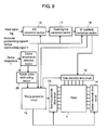
- FIG. 8 is a diagram showing the configuration of a plasma display device as a fourth embodiment of the present invention.
- FIG. 9 is an exploded perspective view of an exemplary configuration of the plasma display device.
- FIG. 10 is a diagram showing an exemplary setting value of a device temperature and that of a sustain pulse width in the plasma display device.
- FIG. 11 is an operation drive timing chart showing a conventional plasma display panel driving method.
- FIG. 1 is a perspective view of main portions of a panel for use in a first embodiment of the present invention.
- Panel 1 has such a configuration that glass-made front and rear substrates 2 and 3 are disposed opposing each other, and a discharge space is formed therebetween.
- Front substrate 2 is formed thereon with scanning electrode 4 and sustain electrode 5 configuring display electrodes, which are disposed in parallel for use as a pair, and such a pair is plurally formed.
- Dielectric layer 6 is formed to cover scanning electrodes 4 and sustain electrodes 5 , and on dielectric layer 6 , protection layer 7 is formed.
- protection layer 7 is preferably made of a material whose secondary electron emission coefficient is high and the sputtering resistance is high, and actually used is a thin film made of magnesium oxide (MgO).
- Rear substrate 3 is provided thereon with a plurality of data electrodes 9 covered by insulator layer 8 , and on insulator layer 8 between data electrodes 9 , partition walls 10 are each disposed in parallel to data electrodes 9 .
- Fluorescent layer 11 is disposed on the surface of insulator layer 8 and the side surfaces of partition walls 10 .
- front substrate 2 and rear substrate 3 are disposed opposing each other and sealed therearound.
- a discharge space formed therebetween is filled with a discharge gas, e.g., a mixture gas of neon (Ne) and xenon (Xe).
- FIG. 2 is a diagram showing the electrode array of the panel shown in FIG. 1 .
- n pieces of scanning electrodes SCN 1 to SCNn scanning electrodes 4 of FIG. 1
- n pieces of sustain electrodes SUS 1 to SUSn sustain electrodes 5 of FIG. 1
- m pieces of data electrodes D 1 to Dm data electrodes 9 of FIG. 1
- FIG. 3 is a diagram showing the configuration of a plasma display device configured by using the panel shown in FIGS. 1 and 2 .
- This plasma display device is configured to include panel 1 , data electrode drive circuit 12 , scanning electrode drive circuit 13 , sustain electrode drive circuit 14 , timing generation circuit 15 , A/D (analog/digital) conversion section 16 , scanning line conversion section 17 , SF (subfield) conversion section 18 , and power supply circuit (not shown).
- a video signal sig is provided to A/D conversion section 16 .
- a horizontal synchronizing signal H and a vertical synchronizing signal V are forwarded to timing generation circuit 15 , A/D conversion section 16 , scanning line conversion section 17 , and SF conversion section 18 .
- A/D conversion section 16 converts the video signal sig into image data of a digital signal, and the resulting image data is output to scanning line conversion section 17 .
- Scanning line conversion section 17 converts the image data into image data suiting the number of pixels of panel 1 , and outputs the result to SF conversion section 18 .
- SF conversion section 18 divides the image data, on a pixel basis, into a plurality of bits corresponding to a plurality of subfields, and outputs the image data of every subfield to data electrode drive circuit 12 .
- Data electrode drive circuit 12 converts the image data, on a subfield basis, into a signal corresponding to each of the data electrodes D 1 to Dm so that the data electrodes D 1 to Dm are driven.
- Timing generation circuit 15 generates a timing signal based on the horizontal synchronizing signal H and the vertical synchronizing signal V, and outputs the signal to both scanning electrode drive circuit 13 and sustain electrode drive circuit 14 . Based on the timing signal, scanning electrode drive circuit 13 supplies a drive waveform to the scanning electrodes SCN 1 to SCNn, and sustain electrode drive circuit 14 supplies a drive waveform to the sustain electrodes SUS 1 to SUSn based on the timing signal.
- FIG. 4 is a diagram showing a drive waveform for application to the scanning electrodes and the sustain electrodes of panel 1 in the first embodiment of the present invention.
- a field period is divided into a plurality of (10 in this example) subfields (1SF, 2SF, . . . , 10SF), and the subfields of 1SF to 10SF have luminance weights of (1, 2, 3, 6, 11, 18, 30, 44, 60, and 80), respectively.
- a field period is so configured that the subfields closer to the tail have the larger luminance weight. Note here that the number of subfields or the luminance weights of the subfields are not restrictive to the above values.
- Each of the subfields has an initialization period in which discharge cells are initialized in charge state, a writing period in which writing discharge is caused for selecting any discharge cell for display (display cells), and a sustain period in which sustain discharge is caused by the discharge cell (s) selected in the writing period.
- an initialization operation of either an every-cell initialization operation or a selective initialization operation is performed.
- every discharge cell is made to perform initial discharge
- any discharge cell (any predetermined discharge cell) through with sustain discharge in the immediately-preceding SF is made to selectively perform initial discharge.
- the charge state of the discharge cells is initialized.
- the every-cell initialization operation is performed in the initialization period of the 1SF, and in the initialization periods of the 2SF to 10SF, the selective initialization operation is performed.
- every discharge cell goes through initial discharge all at once, thereby deleting the previous histories of a wall charge on the respective discharge cells, and forming any needed wall charge for the subsequent writing discharge.
- Every data electrode and every sustain electrode are maintained at 0 (ground potential), and every scanning electrode is applied with a lamp voltage that gently increases from the voltage Vp of a discharge start voltage or lower to the voltage Vr exceeding the discharge start voltage. This causes weak discharge in every discharge cell, stores a positive wall charge on the sustain electrodes and the data electrodes, and stores a negative wall charge on the scanning electrodes.
- every sustain electrode is maintained at the voltage Vh, and every scanning electrode is applied with a lamp voltage that gently decreases from Vg to Va. This causes weak discharge in every discharge cell, and weakens the wall charge stored on the electrodes. With such an every-cell initialization operation, the voltage in the discharge cells is put in the state closer to the discharge start voltage.
- the scanning electrodes are sequentially applied with a scanning pulse, and the data electrodes are applied with a writing pulse corresponding to a video signal for display.
- writing discharge is caused selectively between the scanning electrodes and the data electrodes in any display cell, and a wall charge is selectively formed.
- a sustain pulse (voltage of which is Vm) is applied between the scanning electrodes and the sustain electrodes for a predetermined number of times depending on the luminance weight, and in any discharge cell through with wall charge formation by the writing discharge, sustain discharge is selectively caused for light emission. With such light emission, the video is displayed.
- every sustain electrode is maintained at the voltage Vh, every data electrode is maintained at 0, and every scanning electrode is applied with a lamp voltage that gently decreases from the voltage Vn to the voltage Va.
- this lamp voltage decreases, weak discharge is caused in the discharge cell (s) through with sustain discharge in the immediately-preceding sustain period (sustain period of the 1SF) so that the wall charge formed on the electrodes is weakened, and the voltage in the discharge cells is put in the state closer to the discharge start voltage.
- sustain discharge is caused in any discharge cell corresponding to a video signal.
- the 3SF to 10SF by drive waveform application to the electrodes similarly to the 2SF, the video display is made.
- the sustain period is set as will be described later.
- FIG. 5 shows a drive waveform to be applied to the scanning electrodes and the sustain electrodes in the sustain period of the 1SF of FIG. 4
- FIG. 5 shows the resulting voltage to be applied between the scanning electrodes and the sustain electrodes relative to the sustain electrode.
- the scanning electrodes are applied with a first sustain pulse P 1
- the sustain electrodes are then applied with a second sustain pulse P 2
- the scanning electrodes are then applied with a third sustain pulse P 3
- the sustain electrodes are then applied with a fourth sustain pulse P 4 .
- the scanning electrodes and the sustain electrodes are applied with a voltage with each different timing.
- the sustain discharge accordingly occurs.
- the first sustain pulse P 1 has a width (pulse width) of T 1
- the second sustain pulse P 2 has a width of T 2
- the third sustain pulse P 3 has a width of T 3
- a setting is so made as to establish T 1 >T 2 >T 3
- the fourth sustain pulse P 4 has a width of T 3 .
- the fifth sustain pulse P 5 has a width of T 5 , which is narrower than the width T 3 , and by this sustain pulse P 5 , the sustain discharge occurs lastly in this sustain period, and the sustain discharge is stopped.
- the first sustain pulse P 1 has a width of T 1
- the second sustain pulse P 2 has a width of T 2
- the third sustain pulse has a width of T 3
- a setting is so made as to establish T 1 >T 2 >T 3
- the fourth sustain pulse and subsequent others has a width of T 3
- the last sustain pulse has a width narrower than the width T 3 .
- the 3SF and 4SF are set with the widths of sustain pulses similarly to the 1SF and 2SF.
- the width of the first sustain pulse is set wider than the width of the second sustain pulse, and the width of the second sustain pulse is set wider than the width of the third sustain pulse and subsequent others.
- the width of the sustain pulses is all set to T 3 except the last sustain pulse, and the width of the last sustain pulse is set narrower than the width of T 3 .
- widths T 1 , T 2 , and T 3 of the sustain pulses are assumed as being the same in the 1SF to 4SF, these values may take each different value if the subfields are not the same, e.g., the value of T 1 in the 1SF may be different from the value of T 1 in the 2SF to 4SF.
- the width of the first sustain pulse may be set wider than the width of the second sustain pulse, and the width of the second sustain pulse may be set wider than the width of the third sustain pulse and subsequent others.
- the width of the first sustain pulse in the 1SF to 4SF may be set to a value larger than the width of the first sustain pulse in the 5SF to 10SF, e.g., a value of twice or more. As such, the width of the first sustain pulse in the 1SF to 4SF may be set to be sufficiently large.
- the scanning electrodes may store thereon too much positive wall charge, and the non-display cells (discharge cells of making no display with no image data) may be put in the state that can cause sustain discharge.
- the first sustain pulse is increased in width in the 1SF so that the first sustain pulse can cause sustain discharge (erroneous discharge) in the non-display cells.
- sustain discharge may be delayed by the second sustain pulse to occur, thereby resulting in the insufficient sustain discharge and failing to sustain the sustain discharge.
- the sustain discharge can be sustained with stability. This enables to appropriately adjust the wall charge in the initialization period thereafter (initialization period of 2SF) so that the erroneous discharge is prevented from occurring in the following sustain period (sustain period of 2SF).
- the width of the first sustain pulse is set wider than the width of the second sustain pulse
- the width of the second sustain pulse is set wider than the width of the third sustain pulse and subsequent others.
- the widths of the sustain pulses are set in the 2SF to 4SF, which are subsequent to the subfield (1SF) in charge of the every-cell initialization operation. Accordingly, if such sustain discharge (erroneous discharge) in the non-display cells does not occur in the 1SF even if the scanning electrodes are stored thereon with too much positive wall charge as a result of the every-cell initialization operation (intense discharge) in the 1SF, the sustain discharge (erroneous discharge) can be caused in any one of the 2SF to 4SF. Because these 2SF to 4SF are small in luminance weight, the luminance as a result of erroneous discharge will be low even if such erroneous discharge occurs.
- the erroneous discharge in the non-display cell occurs in any subfield with large luminance weight, the erroneous discharge is not that conspicuous, and the intensity of the erroneous discharge can be controlled to a level of not degrading the display quality.
- the width of the first sustain pulse is set wider than the width of the second sustain pulse
- the width of the second sustain pulse is set wider than the width of the third sustain pulse and subsequent others.
- the subfields in which the sustain pulse is defined by width as such may be 1SF to 3SF or 1SF to 5SF, for example. Such a subfield selection may be made not to cause a problem in terms of display quality even if the erroneous discharge occurs.
- the predetermined subfields may be disposed in a row in a field period, and any one of the predetermined subfields disposed at the head is assigned with the every-cell initialization operation.
- any predetermined number of subfields counted from the subfield with the smallest luminance weight is set as the predetermined subfields, and the number of the predetermined subfields may be a half or less of the entire subfields (10 in this first embodiment).
- the predetermined subfields are not necessarily disposed in ascending order of luminance weight as in the first embodiment.
- the subfields causing the erroneous discharge in the non-display cells are preferably small in luminance weight. Therefore, the subfield in charge of the every-cell initialization operation is the subfield having the smallest luminance weight in the predetermined subfields, and the predetermined subfields are preferably disposed in ascending order of the luminance weight.
- the resulting display quality is good.
- the upper limits of T 1 can be lengthened as long as the drive time permits, and preferably 100 ⁇ s or smaller.
- the width of the first sustain pulse in the sustain periods of the 5SF to 10SF is smaller than T 1 , and may be about 6 ⁇ s.
- the widths of the sustain pulses may be set as in the present embodiment.
- the number of sustain pulses in the subfields having the smaller luminance weight than the 1SF is normally 1 , and this subfield is not counted in the predetermined subfields.
- the voltage having a waveform of showing a gradual voltage value change will do.
- the portion observed with the initial discharge may be applied with the waveform showing a change degree of about 0.1 V/ ⁇ s to 10 V/ ⁇ s.
- FIG. 6 is a diagram showing a drive waveform for application to the scanning electrodes and the sustain electrodes of panel 1 in the second embodiment of the present invention.
- a field period of FIG. 6 is configured by 11 subfields, i.e., 10 subfields same as those in the drive waveform of FIG. 4 plus a subfield having the smaller luminance weight than the 1SF of FIG. 4 . That is, the 2SF to 11SF of FIG. 6 are each have a luminance weight same as that of the 1SF to 10SF of FIG. 4 , and the 1SF of FIG. 6 is the additional subfield.
- the subfields of the 1SF to 11SF have the luminance weights of (0.5, 1, 2, 3, 6, 11, 18, 30, 44, 60, and 80), respectively.
- the subfields each include an initialization period, a writing period, and a sustain period, and the operation in the respective periods is similar to that of the first embodiment.
- the 3SF to 11SF of FIG. 6 have the same waveform as the 2SF to 10SF of FIG. 4 , respectively, and the 2SF of FIG. 6 has the waveform similar to the 1SF of FIG. 4 except the initialization period.
- the every-cell initialization operation is executed in the 1SF, and the selective initialization operation is executed in the 2SF to 11SF.
- the voltage is applied to the scanning electrodes and the sustain electrodes with each different timing so that a single sustain pulse is applied between the scanning electrodes and the sustain electrodes.
- the subfields to be observed with the erroneous discharge are limited to the subfields of low luminance. That is, because the width of the first sustain pulse is made sufficiently wide in the 2SF to 5SF, the first sustain pulse can cause the sustain discharge (erroneous discharge) in the non-display cells. There may be a possibility that, with too wide a width of the first sustain pulse, the sustain discharge may be delayed by the second sustain pulse, thereby resulting in the insufficient sustain discharge and failing to sustain the sustain discharge.
- the sustain discharge can be sustained with stability. This enables appropriate adjustment of the wall charge in the subsequent initialization period so that the sustain discharge is prevented from occurring in any subsequent sustain period. As a result, the erroneous discharge is prevented from occurring in the following subfields having the larger luminance weight so that the display quality can be prevented from being reduced.
- the width of the first sustain pulse is set wider than the width of the second sustain pulse
- the width of the second sustain pulse is set wider than the width of the third sustain pulse and subsequent others.
- the subfields set with the widths of the sustain pulses as such may be the 2SF to 4SF or 2SF to 6SF, i.e., the subfields may be appropriately selected not to cause a problem in terms of display quality even if erroneous discharge occurs.
- the range of T 1 and T 2 the settings similar to the first embodiment will lead to the good display quality.
- FIG. 7 is a diagram showing a drive waveform for application to the scanning electrodes and the sustain electrodes of panel 1 in the third embodiment of the present invention.
- a field period includes 10 subfields, and each of the subfields includes an initialization period, a writing period, and a sustain period.
- the operation in the respective periods is similar to that of the first embodiment.
- a plurality of subfields are in charge of the every-cell initialization operation, and these subfields in charge of the every-cell initialization operation are those with low-luminance. That is, the every-cell initialization operation is performed in the initialization period of the 1SF and 3SF, and the selective initialization operation is performed in the initialization period of the 2SF and the 4SF to 10SF.
- the first sustain pulse P 1 has a width of T 1
- the second sustain pulse P 2 has a width of T 2
- the third sustain pulse P 3 has a width of T 3
- a setting is made so as to establish T 1 >T 2 >T 3 .
- the fourth sustain pulse P 4 and subsequent others have a width of T 3
- the last sustain pulse is set so as to have a width narrower than the width T 3 .
- the width of the sustain pulses is all set to T 3 except the last sustain pulse, and the width of the last sustain pulse is set so as to be smaller than T 3 .
- widths T 1 , T 2 , and T 3 of the sustain pulses are assumed as being the same in the 1SF and 3SF, these values may take each different value if the subfields are not the same, e.g., the value of T 1 in the 1SF may be different from the value of T 1 in the 3SF.
- the width of the first sustain pulse is set wider than the width of the second sustain pulse, and the width of the second sustain pulse is set wider than the width of the third sustain pulse and subsequent others.
- the subfields to be observed with the erroneous discharge can be limited to those with the intense discharge. That is, with the sufficiently wide width of the first sustain pulse, the sustain discharge (erroneous discharge) can be caused in the first sustain pulse in the non-display cells.
- the sustain discharge may be delayed by the second sustain pulse to occur, thereby resulting in the insufficient sustain discharge and failing to sustain the sustain discharge.
- the width of the second sustain pulse is set wider than the width of the third sustain pulse and subsequent others in this embodiment, the sustain discharge can be sustained with stability. This enables to appropriately adjust the wall charge in the initialization period thereafter so that the sustain discharge is prevented from occurring in any subsequent sustain period. As a result, the erroneous discharge is prevented from occurring in the following subfields with the larger luminance weight so that the display quality can be prevented from being reduced.
- a low-luminance subfield may be disposed subsequent to the 1SF or 3SF, and in the low-luminance subfield, the width of the first sustain pulse may be set wider than the width of the second sustain pulse, and the width of the second sustain pulse may be set wider than the width of the third sustain pulse and subsequent others.
- the low-luminance subfield can cause the erroneous discharge even if the sustain discharge (erroneous discharge) in the non-display cells does not occur in the 1SF or 3SF. Because the low-luminance subfield has a small luminance weight, the luminance remains low even if such erroneous discharge occurs.
- the erroneous discharge in the non-display cells occurs in any subfield with large luminance weight, the erroneous discharge is not that conspicuous, and the intensity of the erroneous discharge can be controlled to a level of not degrading the display quality.
- Described in the third embodiment is the exemplary case of performing the every-cell initialization operation in the 1SF and 3SF.
- the present invention is surely not restrictive thereto, and can be applied to a case of performing the every-cell initialization operation in any other low-luminance subfields.
- T 1 and T 2 settings similar to the first embodiment lead to the good display quality.
- FIG. 8 is a diagram showing the configuration of a plasma display device in the fourth embodiment.
- This plasma display device is configured to include panel 1 , data electrode drive circuit 12 , scanning electrode drive circuit 13 , sustain electrode drive circuit 14 , timing generation circuit 15 , A/D conversion section 16 , scanning line conversion section 17 , SF conversion section 18 , power supply circuit (not shown), device temperature detection section 19 , and sustain pulse width setting section 20 .
- provisions of device temperature detection section 19 and sustain pulse width setting section 20 enable to determine and control, based on any change observed to the device temperature, the widths of the first and second sustain pulses in the sustain periods of the respective subfields configuring a field.
- FIG. 9 is an exploded perspective view of an exemplary configuration of a plasma display device.
- the plasma display device is configured by including panel 1 , electric circuit to drive panel 1 or others in a cabinet formed by front cover 21 and rear cover 22 .
- Panel 1 is attached to the front surface side of chassis 23 via thermal conductive sheet 24 , and the rear surface side of chassis 23 is attached with circuit substrate 25 including an electric circuit for driving and controlling panel 1 .
- Chassis 23 is made of metal such as aluminum, and on the rear surface side of chassis 23 , device temperature detection section 19 is disposed to detect temperature of chassis 23 as the device temperature.
- a device temperature T is detected by device temperature detection section 19 , and is then forwarded to sustain pulse width setting section 20 .
- sustain pulse width setting section 20 determines the widths of the first and second sustain pulses in the sustain period of the respective subfields, and timing generation circuit 15 generates a timing signal corresponding to the device temperature T.
- FIG. 10 shows an exemplary relationship between the device temperature T and the widths of the first and second sustain pulses in the sustain periods of the 1SF to 4SF.
- the width of the sustain pulse is so set as be wider as the device temperature T is decreased. This is because the increase of a discharge delay that causes the above-described erroneous discharge becomes apparent as the temperature is decreased.
- the plasma display device can be driven in accordance with the usage environment thereof so that the good display quality can be derived in the low-temperature usage environment.
- the plasma display device is increased in device temperature if it is kept illuminated due to the temperature increase caused by its discharge cells' discharge or the temperature increase of the electric circuit in the illumination state. Accordingly, the discharge delay being apparent with the low-temperature is reduced as the device temperature is increased, and there may be a case of not causing erroneous discharge.
- the drive time tends to have less margin, and this arises a need to shorten the width of the sustain pulse as much as possible, and to reserve the drive time.
- the width of the head sustain pulse in the sustain period of the respective subfields is shortened, and this eliminates the waste of the driving time and enables to reserve the drive time.
- FIG. 10 shows only an exemplary setting of the device temperature and the width of the sustain pulse, and the present invention is surely not restrictive thereto.
- the method of the fourth embodiment is surely applicable.
- the erroneous discharge can be controlled in intensity, and it is considered effective to derive a plasma display panel that performs image display with good quality.
Landscapes
- Engineering & Computer Science (AREA)
- Physics & Mathematics (AREA)
- Computer Hardware Design (AREA)
- General Physics & Mathematics (AREA)
- Theoretical Computer Science (AREA)
- Power Engineering (AREA)
- Plasma & Fusion (AREA)
- Control Of Indicators Other Than Cathode Ray Tubes (AREA)
- Control Of Gas Discharge Display Tubes (AREA)
- Transforming Electric Information Into Light Information (AREA)
Abstract
Description
Claims (10)
Applications Claiming Priority (3)
| Application Number | Priority Date | Filing Date | Title |
|---|---|---|---|
| JP2005050443A JP4665548B2 (en) | 2005-02-25 | 2005-02-25 | Driving method of plasma display panel |
| JP2005-050443 | 2005-02-25 | ||
| PCT/JP2006/303116 WO2006090713A1 (en) | 2005-02-25 | 2006-02-22 | Plasma display panel drive method |
Publications (2)
| Publication Number | Publication Date |
|---|---|
| US20070241994A1 US20070241994A1 (en) | 2007-10-18 |
| US8089426B2 true US8089426B2 (en) | 2012-01-03 |
Family
ID=36927351
Family Applications (1)
| Application Number | Title | Priority Date | Filing Date |
|---|---|---|---|
| US11/628,434 Expired - Fee Related US8089426B2 (en) | 2005-02-25 | 2006-02-22 | Plasma display panel drive method of determining a subfield, having a low luminance, for performing an every-cell initialization operation and setting a width of a sustain pulse of the subfield for performing the every-cell initialization operation |
Country Status (5)
| Country | Link |
|---|---|
| US (1) | US8089426B2 (en) |
| JP (1) | JP4665548B2 (en) |
| KR (2) | KR20070088320A (en) |
| CN (1) | CN101006487B (en) |
| WO (1) | WO2006090713A1 (en) |
Cited By (1)
| Publication number | Priority date | Publication date | Assignee | Title |
|---|---|---|---|---|
| US20110157138A1 (en) * | 2008-09-11 | 2011-06-30 | Panasonic Corporation | Plasma display device and method of driving plasma display panel |
Families Citing this family (5)
| Publication number | Priority date | Publication date | Assignee | Title |
|---|---|---|---|---|
| JPWO2008105160A1 (en) * | 2007-02-27 | 2010-06-03 | パナソニック株式会社 | Driving method of plasma display panel |
| KR20090044778A (en) | 2007-11-01 | 2009-05-07 | 엘지전자 주식회사 | Driving method of plasma display panel and plasma display device using same |
| JPWO2009066423A1 (en) * | 2007-11-19 | 2011-03-31 | パナソニック株式会社 | Plasma display apparatus and driving method of plasma display panel |
| KR101194513B1 (en) * | 2008-09-11 | 2012-10-25 | 파나소닉 주식회사 | Plasma display device and method for driving plasma display panel |
| CN110164348A (en) * | 2018-07-10 | 2019-08-23 | 上海视涯信息科技有限公司 | The drive system of display panel and the display device for applying it |
Citations (19)
| Publication number | Priority date | Publication date | Assignee | Title |
|---|---|---|---|---|
| JPH07134565A (en) | 1993-11-11 | 1995-05-23 | Nec Corp | Method of driving discharge display device |
| JPH08278766A (en) | 1995-04-06 | 1996-10-22 | Fujitsu Ltd | Driving method for flat display panel |
| KR20000053573A (en) | 1999-01-22 | 2000-08-25 | 모리시타 요이찌 | Method for driving AC plasma display panel |
| JP2000242224A (en) | 1999-02-22 | 2000-09-08 | Matsushita Electric Ind Co Ltd | Driving method of AC plasma display panel |
| CN1271155A (en) | 1999-04-20 | 2000-10-25 | 松下电器产业株式会社 | Exciting method for AC type plasma display board |
| JP2001228820A (en) | 2000-02-14 | 2001-08-24 | Mitsubishi Electric Corp | Driving method of plasma display panel and plasma display device |
| JP2001337648A (en) | 2000-05-25 | 2001-12-07 | Pioneer Electronic Corp | Method for driving plasma display panel |
| JP2002006806A (en) | 1999-11-12 | 2002-01-11 | Matsushita Electric Ind Co Ltd | Display device and display method thereof |
| JP2002207449A (en) | 2001-01-12 | 2002-07-26 | Fujitsu Hitachi Plasma Display Ltd | Driving method of plasma display panel |
| US6621230B2 (en) * | 2001-05-10 | 2003-09-16 | Lg Electronics, Inc. | Method for operating PDP |
| US20040012547A1 (en) * | 2002-07-16 | 2004-01-22 | Samsung Sdi Co., Ltd. | PDP driving device and method |
| KR20040023932A (en) | 2002-09-12 | 2004-03-20 | 엘지전자 주식회사 | Driving method and apparatus of plasma display panel |
| US20040164933A1 (en) * | 2003-01-10 | 2004-08-26 | Sebastien Weitbruch | Method for optimizing brightness in a display device and apparatus for implementing the method |
| KR20040093723A (en) * | 2002-02-28 | 2004-11-08 | 쇼와 덴코 가부시키가이샤 | Method for producing cubic boron nitride |
| US20040233131A1 (en) * | 2002-04-18 | 2004-11-25 | Kang Kyoung-Ho | Method of driving a plasma display panel in which the width of display sustain pulse varies |
| US6900781B1 (en) | 1999-11-12 | 2005-05-31 | Matsushita Electric Industrial Co., Ltd. | Display and method for driving the same |
| EP1657702A2 (en) * | 2004-11-16 | 2006-05-17 | Lg Electronics Inc. | Plasma display apparatus and method of driving the same |
| US20060227075A1 (en) * | 2005-04-07 | 2006-10-12 | Kim Nam J | Plasma display panel and apparatus, and driving device and method of plasma display panel |
| US7173850B2 (en) * | 1998-09-10 | 2007-02-06 | Kabushiki Kaisha Toshiba | Nonvolatile semiconductor memory |
-
2005
- 2005-02-25 JP JP2005050443A patent/JP4665548B2/en not_active Expired - Fee Related
-
2006
- 2006-02-22 KR KR1020067026910A patent/KR20070088320A/en not_active Ceased
- 2006-02-22 US US11/628,434 patent/US8089426B2/en not_active Expired - Fee Related
- 2006-02-22 KR KR1020087014872A patent/KR100901893B1/en not_active Expired - Fee Related
- 2006-02-22 WO PCT/JP2006/303116 patent/WO2006090713A1/en not_active Ceased
- 2006-02-22 CN CN2006800006016A patent/CN101006487B/en not_active Expired - Fee Related
Patent Citations (22)
| Publication number | Priority date | Publication date | Assignee | Title |
|---|---|---|---|---|
| JPH07134565A (en) | 1993-11-11 | 1995-05-23 | Nec Corp | Method of driving discharge display device |
| JPH08278766A (en) | 1995-04-06 | 1996-10-22 | Fujitsu Ltd | Driving method for flat display panel |
| US7173850B2 (en) * | 1998-09-10 | 2007-02-06 | Kabushiki Kaisha Toshiba | Nonvolatile semiconductor memory |
| KR20000053573A (en) | 1999-01-22 | 2000-08-25 | 모리시타 요이찌 | Method for driving AC plasma display panel |
| US6294875B1 (en) | 1999-01-22 | 2001-09-25 | Matsushita Electric Industrial Co., Ltd. | Method of driving AC plasma display panel |
| JP2000242224A (en) | 1999-02-22 | 2000-09-08 | Matsushita Electric Ind Co Ltd | Driving method of AC plasma display panel |
| CN1271155A (en) | 1999-04-20 | 2000-10-25 | 松下电器产业株式会社 | Exciting method for AC type plasma display board |
| EP1047041A2 (en) | 1999-04-20 | 2000-10-25 | Matsushita Electric Industrial Co., Ltd. | Method of driving AC plasma display panel |
| US6900781B1 (en) | 1999-11-12 | 2005-05-31 | Matsushita Electric Industrial Co., Ltd. | Display and method for driving the same |
| JP2002006806A (en) | 1999-11-12 | 2002-01-11 | Matsushita Electric Ind Co Ltd | Display device and display method thereof |
| JP2001228820A (en) | 2000-02-14 | 2001-08-24 | Mitsubishi Electric Corp | Driving method of plasma display panel and plasma display device |
| US20020054002A1 (en) | 2000-05-25 | 2002-05-09 | Pioneer Corporation | Method for driving a plasma display panel |
| JP2001337648A (en) | 2000-05-25 | 2001-12-07 | Pioneer Electronic Corp | Method for driving plasma display panel |
| JP2002207449A (en) | 2001-01-12 | 2002-07-26 | Fujitsu Hitachi Plasma Display Ltd | Driving method of plasma display panel |
| US6621230B2 (en) * | 2001-05-10 | 2003-09-16 | Lg Electronics, Inc. | Method for operating PDP |
| KR20040093723A (en) * | 2002-02-28 | 2004-11-08 | 쇼와 덴코 가부시키가이샤 | Method for producing cubic boron nitride |
| US20040233131A1 (en) * | 2002-04-18 | 2004-11-25 | Kang Kyoung-Ho | Method of driving a plasma display panel in which the width of display sustain pulse varies |
| US20040012547A1 (en) * | 2002-07-16 | 2004-01-22 | Samsung Sdi Co., Ltd. | PDP driving device and method |
| KR20040023932A (en) | 2002-09-12 | 2004-03-20 | 엘지전자 주식회사 | Driving method and apparatus of plasma display panel |
| US20040164933A1 (en) * | 2003-01-10 | 2004-08-26 | Sebastien Weitbruch | Method for optimizing brightness in a display device and apparatus for implementing the method |
| EP1657702A2 (en) * | 2004-11-16 | 2006-05-17 | Lg Electronics Inc. | Plasma display apparatus and method of driving the same |
| US20060227075A1 (en) * | 2005-04-07 | 2006-10-12 | Kim Nam J | Plasma display panel and apparatus, and driving device and method of plasma display panel |
Cited By (1)
| Publication number | Priority date | Publication date | Assignee | Title |
|---|---|---|---|---|
| US20110157138A1 (en) * | 2008-09-11 | 2011-06-30 | Panasonic Corporation | Plasma display device and method of driving plasma display panel |
Also Published As
| Publication number | Publication date |
|---|---|
| CN101006487A (en) | 2007-07-25 |
| JP4665548B2 (en) | 2011-04-06 |
| KR20070088320A (en) | 2007-08-29 |
| CN101006487B (en) | 2011-11-09 |
| KR20080064910A (en) | 2008-07-09 |
| US20070241994A1 (en) | 2007-10-18 |
| KR100901893B1 (en) | 2009-06-10 |
| JP2006235292A (en) | 2006-09-07 |
| WO2006090713A1 (en) | 2006-08-31 |
Similar Documents
| Publication | Publication Date | Title |
|---|---|---|
| US8405575B2 (en) | Plasma display device and driving method thereof | |
| JP2004206094A (en) | Driving method of plasma display panel | |
| JP2004021181A (en) | Driving method for plasma display panel | |
| KR20050021877A (en) | Plasma display device and method for driving the same | |
| US7907103B2 (en) | Plasma display apparatus and driving method thereof | |
| JP2005025224A (en) | Method and apparatus for driving plasma display panel | |
| KR100636943B1 (en) | Driving Method of Plasma Display Panel | |
| KR100793483B1 (en) | Driving Method of Plasma Display Panel | |
| KR100784003B1 (en) | Plasma display panel driving method | |
| US8089426B2 (en) | Plasma display panel drive method of determining a subfield, having a low luminance, for performing an every-cell initialization operation and setting a width of a sustain pulse of the subfield for performing the every-cell initialization operation | |
| JP2006003398A (en) | Driving method of plasma display panel | |
| JP2004206093A (en) | Driving method of plasma display panel | |
| JP2007041251A (en) | Driving method of plasma display panel | |
| JP4956911B2 (en) | Driving method of plasma display panel | |
| US20120200543A1 (en) | Driving method of plasma display panel | |
| JP2006284729A (en) | Driving method of AC type plasma display panel | |
| JP2007025635A (en) | Plasma display device and method of treating the same | |
| JP5229233B2 (en) | Plasma display panel driving method and plasma display device | |
| KR100515339B1 (en) | A plasma display panel and a driving method thereof | |
| JP2006003397A (en) | Driving method of plasma display panel | |
| JP2008209683A (en) | Driving method of plasma display device | |
| JP2007041249A (en) | Driving method of plasma display panel | |
| JP2009192651A (en) | Plasma display panel driving method and plasma display device | |
| CN103098117A (en) | Plasma display panel drive method and plasma display device | |
| JP2006195328A (en) | Driving method of plasma display panel |
Legal Events
| Date | Code | Title | Description |
|---|---|---|---|
| AS | Assignment |
Owner name: MATSUSHITA ELECTRIC INDUSTRIAL CO., LTD., JAPAN Free format text: ASSIGNMENT OF ASSIGNORS INTEREST;ASSIGNORS:OGAWA, KENJI;MURAKOSO, TOMOHIRO;TSUJITA, YOSHIKI;AND OTHERS;REEL/FRAME:019765/0369 Effective date: 20061030 |
|
| AS | Assignment |
Owner name: PANASONIC CORPORATION, JAPAN Free format text: CHANGE OF NAME;ASSIGNOR:MATSUSHITA ELECTRIC INDUSTRIAL CO., LTD.;REEL/FRAME:021897/0689 Effective date: 20081001 Owner name: PANASONIC CORPORATION,JAPAN Free format text: CHANGE OF NAME;ASSIGNOR:MATSUSHITA ELECTRIC INDUSTRIAL CO., LTD.;REEL/FRAME:021897/0689 Effective date: 20081001 |
|
| ZAAA | Notice of allowance and fees due |
Free format text: ORIGINAL CODE: NOA |
|
| ZAAB | Notice of allowance mailed |
Free format text: ORIGINAL CODE: MN/=. |
|
| FEPP | Fee payment procedure |
Free format text: PAYOR NUMBER ASSIGNED (ORIGINAL EVENT CODE: ASPN); ENTITY STATUS OF PATENT OWNER: LARGE ENTITY |
|
| STCF | Information on status: patent grant |
Free format text: PATENTED CASE |
|
| FPAY | Fee payment |
Year of fee payment: 4 |
|
| MAFP | Maintenance fee payment |
Free format text: PAYMENT OF MAINTENANCE FEE, 8TH YEAR, LARGE ENTITY (ORIGINAL EVENT CODE: M1552); ENTITY STATUS OF PATENT OWNER: LARGE ENTITY Year of fee payment: 8 |
|
| FEPP | Fee payment procedure |
Free format text: MAINTENANCE FEE REMINDER MAILED (ORIGINAL EVENT CODE: REM.); ENTITY STATUS OF PATENT OWNER: LARGE ENTITY |
|
| LAPS | Lapse for failure to pay maintenance fees |
Free format text: PATENT EXPIRED FOR FAILURE TO PAY MAINTENANCE FEES (ORIGINAL EVENT CODE: EXP.); ENTITY STATUS OF PATENT OWNER: LARGE ENTITY |
|
| STCH | Information on status: patent discontinuation |
Free format text: PATENT EXPIRED DUE TO NONPAYMENT OF MAINTENANCE FEES UNDER 37 CFR 1.362 |
|
| FP | Lapsed due to failure to pay maintenance fee |
Effective date: 20240103 |