US8089232B2 - Motor drive device and semiconductor integrated circuit device - Google Patents
Motor drive device and semiconductor integrated circuit device Download PDFInfo
- Publication number
- US8089232B2 US8089232B2 US12/277,729 US27772908A US8089232B2 US 8089232 B2 US8089232 B2 US 8089232B2 US 27772908 A US27772908 A US 27772908A US 8089232 B2 US8089232 B2 US 8089232B2
- Authority
- US
- United States
- Prior art keywords
- revolutions
- brushless motor
- control
- motor
- signal
- Prior art date
- Legal status (The legal status is an assumption and is not a legal conclusion. Google has not performed a legal analysis and makes no representation as to the accuracy of the status listed.)
- Active, expires
Links
Images


Classifications
-
- H—ELECTRICITY
- H02—GENERATION; CONVERSION OR DISTRIBUTION OF ELECTRIC POWER
- H02P—CONTROL OR REGULATION OF ELECTRIC MOTORS, ELECTRIC GENERATORS OR DYNAMO-ELECTRIC CONVERTERS; CONTROLLING TRANSFORMERS, REACTORS OR CHOKE COILS
- H02P6/00—Arrangements for controlling synchronous motors or other dynamo-electric motors using electronic commutation dependent on the rotor position; Electronic commutators therefor
- H02P6/08—Arrangements for controlling the speed or torque of a single motor
- H02P6/085—Arrangements for controlling the speed or torque of a single motor in a bridge configuration
-
- G—PHYSICS
- G11—INFORMATION STORAGE
- G11B—INFORMATION STORAGE BASED ON RELATIVE MOVEMENT BETWEEN RECORD CARRIER AND TRANSDUCER
- G11B19/00—Driving, starting, stopping record carriers not specifically of filamentary or web form, or of supports therefor; Control thereof; Control of operating function ; Driving both disc and head
- G11B19/20—Driving; Starting; Stopping; Control thereof
- G11B19/2054—Spindle motor power-up sequences
-
- H—ELECTRICITY
- H02—GENERATION; CONVERSION OR DISTRIBUTION OF ELECTRIC POWER
- H02P—CONTROL OR REGULATION OF ELECTRIC MOTORS, ELECTRIC GENERATORS OR DYNAMO-ELECTRIC CONVERTERS; CONTROLLING TRANSFORMERS, REACTORS OR CHOKE COILS
- H02P6/00—Arrangements for controlling synchronous motors or other dynamo-electric motors using electronic commutation dependent on the rotor position; Electronic commutators therefor
- H02P6/14—Electronic commutators
- H02P6/16—Circuit arrangements for detecting position
- H02P6/18—Circuit arrangements for detecting position without separate position detecting elements
- H02P6/181—Circuit arrangements for detecting position without separate position detecting elements using different methods depending on the speed
-
- H—ELECTRICITY
- H02—GENERATION; CONVERSION OR DISTRIBUTION OF ELECTRIC POWER
- H02P—CONTROL OR REGULATION OF ELECTRIC MOTORS, ELECTRIC GENERATORS OR DYNAMO-ELECTRIC CONVERTERS; CONTROLLING TRANSFORMERS, REACTORS OR CHOKE COILS
- H02P6/00—Arrangements for controlling synchronous motors or other dynamo-electric motors using electronic commutation dependent on the rotor position; Electronic commutators therefor
- H02P6/14—Electronic commutators
- H02P6/16—Circuit arrangements for detecting position
- H02P6/18—Circuit arrangements for detecting position without separate position detecting elements
- H02P6/182—Circuit arrangements for detecting position without separate position detecting elements using back-emf in windings
-
- H—ELECTRICITY
- H02—GENERATION; CONVERSION OR DISTRIBUTION OF ELECTRIC POWER
- H02P—CONTROL OR REGULATION OF ELECTRIC MOTORS, ELECTRIC GENERATORS OR DYNAMO-ELECTRIC CONVERTERS; CONTROLLING TRANSFORMERS, REACTORS OR CHOKE COILS
- H02P6/00—Arrangements for controlling synchronous motors or other dynamo-electric motors using electronic commutation dependent on the rotor position; Electronic commutators therefor
- H02P6/14—Electronic commutators
- H02P6/16—Circuit arrangements for detecting position
- H02P6/18—Circuit arrangements for detecting position without separate position detecting elements
- H02P6/187—Circuit arrangements for detecting position without separate position detecting elements using the star point voltage
Definitions
- the present invention relates to a motor drive control technique and, particularly, to a technique that is effective for control of revolution of a multi-phase brushless motor for use in a hard disk drive (HDD) or the like.
- HDD hard disk drive
- a spindle motor is widely used to drive a magnetic disk in a hard disk system or the like.
- the spindle motor comprises a brushless DC multi-phase motor and the spindle motor is driven by, for example, an IC dedicated to driving the motor (motor drive IC) and spins the magnetic disk at a high speed.
- PWM Pulse Width Modulation
- BEMF back electromotive force
- the motor drive IC that performs such soft switching control includes an output section which is comprised of, for example, a plurality of power MOS (Metal Oxide Semiconductor) transistors and a predriver and drives a spindle motor, a DC current detecting section which detects a motor drive current, a BEMF detecting section which detects the back electromotive force of the spindle motor, an A/D (Analog/Digital) converter which converts a voltage appearing in a DC current or a non-conducting phase out of three phases into a digital value, and a logic section.
- MOS Metal Oxide Semiconductor
- the logic section includes a PLL (Phase Locked Loop) control loop, a current control loop, a soft switching controller which suppresses a steep change in current, a serial port which receives a command from an MPU (Micro Processing Unit), resisters, and others.
- PLL Phase Locked Loop
- MPU Micro Processing Unit
- the spindle motor is driven by 120 deg conduction for which there is no need for generating a voltage profile with asynchronous PWM. This gives rise to a problem of a high noise level during a startup.
- the predriver and the zero cross detecting circuit become very difficult to design with a PWM frequency in the order of 200 kHz, for example. Furthermore, a decrease in power efficiency due to switching loss is not negligible.
- An object of the present invention it to provide a technique that allows for a significant reduction in the noise and vibration of a brushless motor from startup up to the number of steady revolutions.
- One aspect of the present invention resides in a motor drive device that switches a current to flow in each of the phases of a brushless motor having a plurality of coils and drives the brushless motor
- the motor derive device comprising a motor drive control mechanism that performs control processing, switching between a first mode of soft switching control with an asynchronous PWM carrier signal independent of the number of revolutions of the brushless motor and a second mode of soft switching control with a synchronous PWM carrier signal synchronized with the number of revolutions of the brushless motor.
- the motor drive control mechanism performs soft switching control with an asynchronous PWM carrier signal independent of the number of revolutions of the brushless motor from a startup of the brushless motor up to an arbitrarily set number of revolutions and performs soft switching control with a synchronous PWM carrier signal synchronized with the number of revolutions of the brushless motor when the brushless motor runs at the arbitrarily set number of revolutions or higher.
- the arbitrarily set number of revolutions of the brushless motor comprises the number of steady revolutions of the brushless motor.
- the motor drive control mechanism comprises a common arithmetic unit that executes an arithmetic operation for a PLL control loop for the brushless motor, an arithmetic operation for a current control loop, and an arithmetic operation for soft switching control to suppress a steep change in current; a turn-on timing counter that generates a conducting phase signal from a result of the arithmetic operation for a PLL control loop; an output controller that generates a PWM signal to control a current to be supplied to the brushless motor; and a control unit that detects the number of revolutions of the brushless motor.
- the control unit activates a synchronization/no synchronization control signal indicating whether to synchronize the PWM carrier signal frequency with the number of revolutions of the brushless motor or fix the frequency, when the number of revolutions of the brushless motor is less than the number of steady revolutions, and deactivates the synchronization/no synchronization control signal, when the number of revolutions of the brushless motor has reached the number of steady revolutions.
- the common arithmetic unit detects whether a division control signal which is a synchronous PWM carrier signal count value generated by the turn-on timing counter has changed when the synchronization/no synchronization control signal is active and executes soft switch arithmetic upon detecting a change of the division control signal.
- Yet another aspect of the present invention resides in a semiconductor integrated circuit device for driving a motor, wherein the semiconductor integrated circuit device switches a current to flow in each of the phases of a brushless motor having a plurality of coils and drives the brushless motor, the semiconductor integrated circuit device comprising a motor drive control mechanism that performs control processing, switching between a first mode of soft switching control with an asynchronous PWM carrier signal independent of the number of revolutions of the brushless motor and a second mode of soft switching control with a synchronous PWM carrier signal synchronized with the number of revolutions of the brushless motor.
- the motor drive control mechanism performs soft switching control with an asynchronous PWM carrier signal independent of the number of revolutions of the brushless motor from a startup of the brushless motor up to an arbitrarily set number of revolutions and performs soft switching control with a synchronous PWM carrier signal synchronized with the number of revolutions of the brushless motor when the brushless motor runs at the arbitrarily set number of revolutions or higher.
- the arbitrarily set number of revolutions of the brushless motor comprises the number of steady revolutions of the brushless motor.
- the motor drive control mechanism comprises a common arithmetic unit that executes an arithmetic operation for a PLL control loop for the brushless motor, an arithmetic operation for a current control loop, and an arithmetic operation for soft switching control to suppress a steep change in current; a turn-on timing counter that generates a conducting phase signal from a result of the arithmetic operation for a PLL control loop; an output controller that generates a PWM signal to control a current to be supplied to the brushless motor; and a control unit that detects the number of revolutions of the brushless motor.
- the control unit activates a synchronization/no synchronization control signal indicating whether to synchronize the PWM carrier signal frequency with the number of revolutions of the brushless motor or fix the frequency, when the number of revolutions of the brushless motor is less than the number of steady revolutions, and deactivates the synchronization/no synchronization control signal, when the number of revolutions of the brushless motor has reached the number of steady revolutions.
- the common arithmetic unit detects whether a division control signal which is a synchronous PWM carrier signal count value generated by the turn-on timing counter has changed when the synchronization/no synchronization control signal is active and executes soft switch arithmetic upon detecting a change of the division control signal.
- FIG. 1 is a block diagram of a motor driving device according to one embodiment of the invention.
- FIG. 2 illustrates an exemplary drive waveform of a pseudo sine wave for explaining an example of soft switching drive control by a soft switch controller.
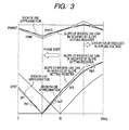
- FIG. 3 is a graph for explaining an example of calculating a voltage profile according to one embodiment of the invention.
- FIG. 4 is a block diagram showing a configuration of a common arithmetic unit and its peripheral blocks connected thereto, provided in the motor driving device shown in FIG. 1 .
- FIG. 5 is a flowchart illustrating an exemplary operation of the common arithmetic unit shown in FIG. 4 .
- FIG. 6 is a flowchart following the one shown in FIG. 5 .
- FIG. 7 is graph for explaining a relationship between the number of revolutions of a three-phase brushless motor and PWM frequency, according to one embodiment of the invention.
- FIG. 8 is a diagram for explaining an exemplary voltage profile created by the common arithmetic unit shown in FIG. 4 .
- FIG. 9 is a block diagram of a motor driving device according to another embodiment of the invention.
- FIG. 10 illustrates an exemplary operating waveform of the motor driving device shown in FIG. 9 .
- FIG. 1 is a block diagram of a motor driving device according to one embodiment of the present invention.
- FIG. 2 illustrates an exemplary drive waveform of a pseudo sine wave for explaining an example of soft switching drive control by a soft switch controller.
- FIG. 3 is a graph for explaining an example of calculating a voltage profile.
- FIG. 4 is a block diagram showing a configuration of a common arithmetic unit and its peripheral blocks connected thereto, provided in the motor driving device shown in FIG. 1 .
- FIG. 5 is a flowchart illustrating an exemplary operation of the common arithmetic unit shown in FIG. 4 .
- FIG. 6 is a flowchart following the one shown in FIG. 5 .
- FIG. 7 is a graph for explaining a relationship between the number of revolutions of a three-phase brushless motor and PWM frequency.
- FIG. 8 is a diagram for explaining an exemplary voltage profile created by the common arithmetic unit shown in FIG. 4 .
- the motor driving device 1 controls driving of a three-phase brushless motor M such as a spindle motor which is used in, e.g., a hard disk drive.
- the motor driving device 1 is comprised of a current output circuit 2 , an output controller 3 , a soft switch controller 4 , a selector 5 , a preamplifier 6 , a filter 7 , a comparator 8 , a phase error detector 9 , a PLL filter 10 , a turn-on timing counter 11 , a DC shunt resistor 12 , a sample and hold circuit 13 , a differential amplifier for output current detection 15 , a current control filter 16 , an MPU 17 , a serial port 18 , a parameter setting register 19 , a selector 20 , an A/D converter 21 , a conducting phase controller 22 , a sequencer 23 , and a common arithmetic unit 24 .
- the current output circuit 2 is comprised of an output section 2 a and an output predriver 2 b and causes a current to flow in coils Lu, Lv, Lw of the three-phase brushless motor M in order.
- the output section 2 a is comprised of transistors M 1 to M 6 which comprise power MOSFETs (Field Effect Transistors) or the like.
- the three-phase brushless motor M is driven by a pulse width modulated (PWM) signal output by the output section 2 a and the output predriver 2 b .
- PWM pulse width modulated
- the output controller 3 which forms a part of a motor drive control mechanism generates and supplies a PWM signal that drives the transistors M 1 to M 6 in the current output circuit 2 and controls an output current.
- the output controller 3 also outputs to the selector 5 a control signal to select a coil terminal at which the back electromotive force should be detected.
- the output predriver 2 b operates with inputs of PWM modulated signals UP, UN, VP, VN, WP, WN which are results of PWM modulation, in the output controller 3 , of a sine-wave drive voltage generated by the soft switch controller 4 .
- the soft switch controller 4 controls conducting phase switching so that two conducting phases are PWM modulated, thereby smoothing current switching.
- FIG. 2 illustrates an exemplary drive waveform of a pseudo sine (sin) wave for explaining an example of soft switching drive control by the soft switch controller 4 .
- the drive waveform is placed in a non-conducting state only when a zero cross of the BEMF back electromotive force is detected.
- a voltage profile SP 1 by soft switch control followed by PWM by current control, a voltage profile SP 2 by soft switch control, and a non-conducting period for zero cross detection are repeated.
- a mask signal MASK is used to control a period of BEMF back electromotive force zero cross detection.
- a Lo MASK signal corresponds to a BEMF detection period.
- initial values (PWMST, SPST) of drive voltage patterns are calculated from a drive current and an amount of phase shift determined by a phase setting register, as shown in FIG. 3 .
- a differential voltage of the selected phase with respect to a neutral point CT of the motor coils is generated by the preamplifier 6 .
- An output signal of the preamplifier 6 after filtered by the filter 7 , is compared to a reference voltage Vref 1 by the comparator 8 .
- the BEMF back electromotive force
- the result of the zero cross detection is input to the phase error detector 9 .
- An output signal of the phase error detector 9 passes through a PLL control loop which is comprised of the PLL filter 10 , the turn-on timing counter 11 , the output controller 3 , the current output circuit 2 , and the three-phase brushless motor M.
- the PLL control loop provides motor driving with a low revolution jitter.
- Detecting a motor drive current for the three-phase brushless motor M is done by using the DC shunt resistor 12 .
- a voltage detected by the DC shunt resistor 12 passes through the sample and hold circuit 13 and is amplified by the differential amplifier for output current detection and A/D converted.
- an error is calculated by the error current detector 15 , based on a current command SPN CRNT DATA.
- the drive current is controlled through a current control loop comprised of the current control filter 16 , the output controller 3 , the current output circuit 2 , and the three-phase brushless motor M.
- a period signal PHASE that is proportional to the number of revolutions is output by the output controller 3 to the MPU 17 which is a microprocessor.
- the MPU 17 which forms a part of the motor drive control mechanism and serves as a control unit compares the motor speed to a target speed, based on the period signal PHASE, and issues a current command depending on the speed.
- Arithmetic processing for these PLL control, current control, and soft switch control is performed by the common arithmetic unit 24 in which an arithmetic processor is shared.
- the serial port 18 interfaces with the MPU 17 .
- Parameters such as current command data SPN CRNT DATA, current control, PLL, and constant torque driving are set by the parameter setting register 19 .
- a signal from which noise has been eliminated by the filter 7 is supplied via the selector 20 to the A/D converter 21 and converted into a digital signal.
- the device includes the conducting phase controller 22 that controls a startup of the three-phase brushless motor M from the stopped state and the sequencer 23 controls internal operation, as a spindle drive related system.
- FIG. 4 is a block diagram showing a configuration of the common arithmetic unit 24 and its peripheral blocks connected thereto.
- the common arithmetic unit 24 which forms a part of the motor drive control mechanism is comprised of a PLL arithmetic register 25 , a current control register 26 , a soft switch register 27 , an arithmetic processor 28 , a common register 29 , selectors 30 , 31 , and an arithmetic sequencer 32 .
- the PLL arithmetic register 25 To the input terminals of a selector 30 , the PLL arithmetic register 25 , the current control register 26 , and the soft switch register 27 are connected, so that arithmetic results stored in these registers are input to the selector 30 .
- the A/D converter 21 To the input terminals of the selector 30 , further, the A/D converter 21 , a phase comparator register provided in the phase error detector 9 , and the parameter setting register 19 are connected, so that converted data from the A/D converter, a register value from the phase comparator register, and parameter values set in the parameter setting register 19 are input to the selector 30 .
- a selector 32 c of the arithmetic sequencer 32 which will be described later, is connected, so that a control signal (clock signal BSTCLK or clock signal VCOCLK) output from the selector 32 c is input to the selector 30 .
- the selector 30 selects an arbitrary input terminal and outputs the value received at the input terminal from an output terminal of the selector 30 .
- the common register 29 is connected to the output terminal of the selector 30 .
- the arithmetic processor 28 is connected to the common register 29 .
- An output terminal of the arithmetic processor 28 is connected to the common register 29 , the PLL arithmetic register 25 , the current control register 26 , and the soft switch register 27 , so that an arithmetic result of the arithmetic processor 28 is output to the appropriate one of these registers.
- the arithmetic sequencer 32 is comprised of arithmetic sequences 32 a , 32 b , and a selector 32 c.
- the selector 32 c selects either of arithmetic results of the arithmetic sequence 32 a and the arithmetic sequence 32 b , based on a control signal PWMSYNC which is input externally via the serial port 18 , and outputs the arithmetic result to the selector 30 , the arithmetic processor 28 , the PLL arithmetic register 25 , the current control register 26 , and the soft switch register 27 .
- a control signal PWMSYNC which is a synchronization/no synchronization control signal indicates whether to synchronize the PWM signal frequency with the number of revolutions of the motor M or fix the frequency.
- Arithmetic results of PLL control, current control, and soft switch control are controlled by this arithmetic sequencer 32 and stored into the PLL arithmetic register 25 , the current control register 26 , and the soft switch register 27 , respectively.
- the turn-on timing counter 11 which forms a part of the motor drive control mechanism is comprised of a carrier counter 11 a , a 60 deg counter 11 b , and a phase switch counter 11 c .
- the turn-on timing counter 11 generates a conducting phase signal from the PLL arithmetic result stored in the PLL arithmetic register 25 , using the carrier counter 11 a , the 60 deg counter 11 b , and the phase switch counter 11 c.
- the carrier counter 11 a generates a clock signal VCOCLK serving as a synchronous PWM carrier signal from the PLL arithmetic result stored in the PLL arithmetic register 25 (the cycle count value of the clock signal VCOCLK).
- the 60 deg counter 11 b is a divide-by-16 or divide-by-32 counter.
- the 60 deg counter 11 b generates a divisional signal fcom with a cycle of 60 deg from the clock signal VCOCLK and outputs this signal fcom as well as a division control signal DIVCNT which is a count value of the divisional signal fcom to the phase switch counter 11 c.
- the output controller 3 is comprised of selectors 3 a , 3 b , a carrier counter 3 c , a PWM modulator 3 d , an SP modulator 3 e , and a PWM pulse generator 3 f .
- the arithmetic sequencer 32 is comprised of arithmetic sequences 32 a , 32 b , and a selector 32 c.
- a control signal PWMSYNC is input.
- a count value (clock signal VCOCLK of the carrier counter 11 a and a fixed carrier count value are input, respectively.
- the current control register 26 is connected.
- the carrier counter 3 c and the carrier counter 11 a are connected, so that count values of these counters are input to the selector 3 b , respectively.
- the PWM modulator 3 d and the SP modulator 3 e are connected.
- the PWM modulator 3 d and the SP modulator 3 e are connected, so that a PWM signal modulated by the PWM modulator 3 d and voltage profiles SP 1 , SP 2 modulated by the SP modulator 3 e are input to the PWM pulse generator 3 f , respectively.
- a soft switch enable signal SOFTENA is input.
- the PWM pulse generator 3 f performs soft switching control using the output of the SP modulator 3 e , when the soft switch enable signal SOFTENA becomes active (e.g., Hi level).
- a clock signal BSTCLK generated by the carrier counter 3 c and a clock signal VCOCLK generated by the carrier counter 11 a are input, respectively.
- a control signal PWMSYNC which is input externally is input.
- the selector 31 feeds either the clock signal BSTCLK or the clock signal VCOCLK to the arithmetic sequencer 32 as a PWM carrier signal CARYCLK.
- the arithmetic sequencer 32 executes an iterative calculation based on the PWM carrier signal CARYCLK input thereto.
- the selector 3 b selects and outputs either the count value of the carrier counter 11 a or the count value of the carrier counter 3 c to the PWM modulator 3 d and the SP modulator 3 e.
- the PWM modulator 3 d compares the count value of the carrier counter 3 c and the arithmetic result obtained (the number of ON counts of PWM signal (the number of PWM ON counts) stored in the current control register 26 ), executes PWM modulation, and creates a PWM signal.
- the SP modulator 3 e compares the count value of the carrier counter 3 c and the arithmetic result obtained (the number of ON counts of voltage profile (the number of SP ON counts) stored in the soft switch register 27 ) and creates voltage profiles SP 1 , SP 2 .
- the PWM pulse generator 3 f generates a predriver drive signal from the conducting phase signal output from the phase switch counter 11 c , the PWM signal output from the PWM modulator 3 d , and the voltage profiles SP 1 , SP 2 output from the SP modulator 3 e.
- the three-phase brushless motor M is driven according to the steps in the flowchart shown in FIG. 5 from its stopped state (0%) up to steady run state (100%), wherein a large current is required for startup and a control signal PWMSYNC which is Lo level (active) is input, as shown in FIG. 7 .
- the selector 3 a selects a fixed carrier count value
- the selector 3 b selects an output signal of the carrier counter 3 c
- the selector 31 selects a clock signal BSTCLK.
- a fixed frequency of about 120 kHz is assumed.
- the control signal PWMSYNC is turned high (Hi level).
- the operation switches to a synchronization mode in which the PWM carrier frequency is synchronized with the number of revolutions of the motor, so that the motor runs with low noise and low revolution jitter (PWM frequency is 69 kHz).
- step S 101 when the arithmetic sequencer 32 detects a rise of a clock signal CARYCLK (step S 101 ), current control arithmetic is executed.
- the arithmetic sequencer 32 controls the selector 30 to load data output from the A/D converter 21 and data (current command data SPNCRNT and a fixed carrier count value) set in the parameter setting register 19 into the common register 29 .
- the arithmetic sequencer 32 also controls the operation mode of the arithmetic processor 28 to store its arithmetic result into the current control register 26 (step S 102 ).
- step S 104 the arithmetic sequence 32 b determines whether a division control signal DIVCNT has changed.
- step S 105 soft switch arithmetic is executed.
- the arithmetic sequencer 32 controls the selector 30 to load data output from the A/D converter 21 , data (current command data SPNCRNT, a soft switch parameter) set in the parameter setting register 19 , and data from the current control register 26 into the common register 29 .
- the arithmetic sequencer 32 also controls the operation mode of the arithmetic processor 28 to store its arithmetic result into the soft switch register 27 .
- step S 106 which will be described below is executed.
- the arithmetic sequencer 32 determines whether a rise of a mask signal MASK has occurred during one cycle of the PWM carrier signal CARYCLK (step S 106 ). If a rise of the mask signal MASK has not occurred, the operation returns to the step S 101 .
- step S 107 PLL control arithmetic is executed (step S 107 ), then the operation returns to the step S 101 .
- the arithmetic sequencer 32 controls the selector 30 to load data from the phase comparator register of the phase error detector 9 and data from the PLL arithmetic register 25 into the common register.
- the arithmetic sequencer 32 also controls the operation mode of the arithmetic processor 28 to store its arithmetic result into the PLL arithmetic register 25 .
- the process of FIG. 6 is carried out in the synchronization mode in which the PWM carrier frequency is synchronized with the number of revolutions of the motor, so that the motor runs with low noise and low revolution jitter.
- a clock signal VCOCLK is selected as the clock signal CARYCLK by the selector 31 .
- these steps S 201 to S 206 are to be repeated.
- FIG. 8 is a diagram for explaining an exemplary voltage profile which is created by applying the present invention.
- a voltage profile is created by adding and subtracting an amount of voltage (dpwm, dps 1 , dps 2 , dps 3 ) which changes for each cycle of the clock signal VCOCLK to/from a voltage pattern value for every clock signal VCOCLK (or clock signal BSTCLK) for broken line approximation.
- the update interval of is shortest and the arithmetic sequence of current control arithmetic is calculated iteratively on the basis of a PWM carrier signal CARYCLK.
- current control arithmetic is calculated once for every PWM carrier signal CARYCLK.
- PLL arithmetic is executed when the mask signal changes from Lo level to Hi level, that is, only after the completion of BEMF detection.
- Soft switch arithmetic is triggered by detecting a change of the division control signal DIVCNT and executed only once for one cycle of the division control signal DIVCNT, and the voltage profile is synchronized with the number of revolutions.
- a ripple in the supply current can be reduced, since the PWM carrier frequency can be fixed when the motor is initially accelerated, wherein the acceleration requires a large current.
- Soft switching control becomes possible from a low revolution and, therefore, it is possible to start up the three-phase brushless motor M with low noise.
- the present invention may be applied to, for example, a motor driving device 1 a by 180 deg conduction, which is shown in FIG. 9 .
- the motor driving device 1 a further includes comparators 33 , 34 , selectors 35 , 36 , and a sample/hold circuit 37 added to the configuration of the motor driving device 1 shown in FIG. 1 .
- one of U, V, W phases of an output voltage to the spindle motor is selected by the selector 5 as the phase for which the BEMF back electromotive force should be detected.
- a differential voltage of the selected phase with respect to a neutral point CT of the motor coils is generated by the preamplifier 6 .
- An output signal of the preamplifier 6 after being filtered by the filter 7 , is compared to a reference voltage Vref 1 by the comparator 8 .
- the BEMF back electromotive force
- One of gate voltages UL, VL, WL of lower transistors M 2 , M 4 , M 6 in the half bridge output stage is selected by the selector 35 as the phase for which a current zero cross should be detected.
- the current zero cross is detected as follows: the comparator 33 detects the timing at which the output of the selector 5 intersects with a reference voltage Vref 3 , the output of the selector 35 is sampled and held by the sample/hold circuit 37 , and this voltage is compared to a reference voltage Vref 2 by the comparator 34 .
- the detected current zero cross should be used if constant torque driving is performed; otherwise, the detected BEMF zero cross should be used.
- FIG. 10 illustrates an exemplary operating waveform of the motor driving device 1 a shown in FIG. 9 .
- a voltage that is applied to the motor coils is a voltage obtained by subtracting the BEMF from the drive voltage. If the BEMF is a sine wave, the voltage applied to the motor coils is also a sine wave. Hence, the drive current is a sine wave, making it possible to drive the motor at a constant toque. Consequently, a constant motor torque and the motor running with low noise and low vibration can be achieved.
- a difference only lies in the method of detecting a BEMF phase.
- a voltage profile is generated in the same way as in FIG. 10 , enabling 180 deg conduction, and the present invention can be applied.
- the present invention is suitable for a technique for a startup of a multi-phase brushless motor with low noise and low vibration.
Landscapes
- Engineering & Computer Science (AREA)
- Power Engineering (AREA)
- Control Of Motors That Do Not Use Commutators (AREA)
Abstract
Description
- Japanese Unexamined Patent Publication No. 2005-278386
Claims (10)
Applications Claiming Priority (2)
| Application Number | Priority Date | Filing Date | Title |
|---|---|---|---|
| JP2008-014415 | 2008-01-25 | ||
| JP2008014415A JP5253828B2 (en) | 2008-01-25 | 2008-01-25 | Motor driving device and semiconductor integrated circuit device |
Publications (2)
| Publication Number | Publication Date |
|---|---|
| US20090189556A1 US20090189556A1 (en) | 2009-07-30 |
| US8089232B2 true US8089232B2 (en) | 2012-01-03 |
Family
ID=40898531
Family Applications (1)
| Application Number | Title | Priority Date | Filing Date |
|---|---|---|---|
| US12/277,729 Active 2029-12-17 US8089232B2 (en) | 2008-01-25 | 2008-11-25 | Motor drive device and semiconductor integrated circuit device |
Country Status (2)
| Country | Link |
|---|---|
| US (1) | US8089232B2 (en) |
| JP (1) | JP5253828B2 (en) |
Cited By (7)
| Publication number | Priority date | Publication date | Assignee | Title |
|---|---|---|---|---|
| US20120074876A1 (en) * | 2010-02-01 | 2012-03-29 | Redler Yesaiahu | Apparatus and method for optimizing current use during control of multiple motors |
| US20120169264A1 (en) * | 2011-01-05 | 2012-07-05 | Texas Instruments Incorporated | Method and apparatus for commutating a brushless dc motor |
| US20130093377A1 (en) * | 2011-10-05 | 2013-04-18 | Renesas Electronics Corporation | Pwm output apparatus and motor driving apparatus |
| US20130175956A1 (en) * | 2012-01-06 | 2013-07-11 | Samsung Electronics Co., Ltd. | Apparatus and method to control bldc motor |
| US20140056338A1 (en) * | 2012-08-27 | 2014-02-27 | Fanuc Corporation | Data communication device that carries out serial communication in order to control motor |
| US20170025972A1 (en) * | 2015-07-24 | 2017-01-26 | Anpec Electronics Corporation | Control apparatus for eliminating magnetizing error of rotor in dc motor and method thereof |
| US20170170756A1 (en) * | 2014-09-12 | 2017-06-15 | Panasonic Intellectual Property Management Co., Lt d. | Pwm motor drive device |
Families Citing this family (9)
| Publication number | Priority date | Publication date | Assignee | Title |
|---|---|---|---|---|
| US8030867B1 (en) * | 2006-07-29 | 2011-10-04 | Ixys Ch Gmbh | Sample and hold time stamp for sensing zero crossing of back electromotive force in 3-phase brushless DC motors |
| EP2133988B1 (en) * | 2007-03-30 | 2019-03-13 | Shindengen Electric Manufacturing Co., Ltd. | Brushless motor control device and brushless motor controlling method |
| FR3007911B1 (en) * | 2013-06-27 | 2015-06-26 | Somfy Sas | DEVICE FOR CONTROLLING AN ENGINE |
| JP6189662B2 (en) * | 2013-07-22 | 2017-08-30 | ローム株式会社 | MOTOR DRIVE DEVICE, DRIVE METHOD, COOLING DEVICE, ELECTRONIC DEVICE |
| JP2018046628A (en) * | 2016-09-13 | 2018-03-22 | 株式会社東芝 | Brushless DC motor control device and brushless DC motor device |
| CN108448949A (en) * | 2018-03-12 | 2018-08-24 | 哈尔滨工大航博科技有限公司 | Dual-motor dual-driver parallel synchronous drive system applied to turntable system |
| JP7169816B2 (en) * | 2018-08-20 | 2022-11-11 | ローム株式会社 | Motor driver device and semiconductor device |
| JP7204409B2 (en) * | 2018-10-11 | 2023-01-16 | ローム株式会社 | motor driver device |
| JP7352492B2 (en) * | 2020-03-02 | 2023-09-28 | ルネサスエレクトロニクス株式会社 | Semiconductor device and motor drive system using it |
Citations (5)
| Publication number | Priority date | Publication date | Assignee | Title |
|---|---|---|---|---|
| US4860186A (en) * | 1987-11-12 | 1989-08-22 | Kabushiki Kaisha Toshiba | PWM controller having synchronous and asynchronous mode |
| US20050046369A1 (en) * | 2003-08-25 | 2005-03-03 | Aisin Aw Co., Ltd. | Electric drive control apparatus, electric drive control method and program thereof |
| JP2005278386A (en) | 2004-02-26 | 2005-10-06 | Renesas Technology Corp | Motor driving device and integrated circuit device for driving motor |
| US20060049792A1 (en) * | 2004-09-09 | 2006-03-09 | Aisin Aw Co., Ltd. | Motor drive control apparatus, motor drive control method and program of the same |
| US20070064454A1 (en) * | 2005-09-21 | 2007-03-22 | Chen Isaac Y | Circuit and method for soft start from a residual voltage |
Family Cites Families (6)
| Publication number | Priority date | Publication date | Assignee | Title |
|---|---|---|---|---|
| JPH114600A (en) * | 1997-06-11 | 1999-01-06 | Hitachi Ltd | Drive system for electric vehicles |
| JP2003169490A (en) * | 2001-12-03 | 2003-06-13 | Mitsubishi Heavy Ind Ltd | Motor control system, motor control apparatus, and control method of motor-driving inverter |
| JP3912190B2 (en) * | 2002-05-31 | 2007-05-09 | 松下電器産業株式会社 | Brushless motor drive device and motor using the same |
| JP2005086920A (en) * | 2003-09-09 | 2005-03-31 | Fuji Electric Systems Co Ltd | Control method for synchronous motor drive device |
| JP4420317B2 (en) * | 2003-09-26 | 2010-02-24 | 株式会社ルネサステクノロジ | Motor driving device and integrated circuit device for motor driving |
| JP4583111B2 (en) * | 2004-08-31 | 2010-11-17 | ルネサスエレクトロニクス株式会社 | Motor drive control device and disk rotation system |
-
2008
- 2008-01-25 JP JP2008014415A patent/JP5253828B2/en not_active Expired - Fee Related
- 2008-11-25 US US12/277,729 patent/US8089232B2/en active Active
Patent Citations (6)
| Publication number | Priority date | Publication date | Assignee | Title |
|---|---|---|---|---|
| US4860186A (en) * | 1987-11-12 | 1989-08-22 | Kabushiki Kaisha Toshiba | PWM controller having synchronous and asynchronous mode |
| US20050046369A1 (en) * | 2003-08-25 | 2005-03-03 | Aisin Aw Co., Ltd. | Electric drive control apparatus, electric drive control method and program thereof |
| JP2005278386A (en) | 2004-02-26 | 2005-10-06 | Renesas Technology Corp | Motor driving device and integrated circuit device for driving motor |
| US6998801B2 (en) | 2004-02-26 | 2006-02-14 | Renesas Technology Corp. | Motor drive device and motor drive integrated circuit device |
| US20060049792A1 (en) * | 2004-09-09 | 2006-03-09 | Aisin Aw Co., Ltd. | Motor drive control apparatus, motor drive control method and program of the same |
| US20070064454A1 (en) * | 2005-09-21 | 2007-03-22 | Chen Isaac Y | Circuit and method for soft start from a residual voltage |
Cited By (15)
| Publication number | Priority date | Publication date | Assignee | Title |
|---|---|---|---|---|
| US8629634B2 (en) * | 2010-02-01 | 2014-01-14 | Yesaiahu REDLER | Apparatus and method for optimizing current use during control of multiple motors |
| US20120074876A1 (en) * | 2010-02-01 | 2012-03-29 | Redler Yesaiahu | Apparatus and method for optimizing current use during control of multiple motors |
| US20120169264A1 (en) * | 2011-01-05 | 2012-07-05 | Texas Instruments Incorporated | Method and apparatus for commutating a brushless dc motor |
| US9374032B2 (en) | 2011-10-05 | 2016-06-21 | Renesas Electronics Corporation | PWM output apparatus and motor driving apparatus |
| US8816621B2 (en) * | 2011-10-05 | 2014-08-26 | Renesas Electronics Corporation | PWM output apparatus and motor driving apparatus |
| US20130093377A1 (en) * | 2011-10-05 | 2013-04-18 | Renesas Electronics Corporation | Pwm output apparatus and motor driving apparatus |
| US20130175956A1 (en) * | 2012-01-06 | 2013-07-11 | Samsung Electronics Co., Ltd. | Apparatus and method to control bldc motor |
| US9054614B2 (en) * | 2012-01-06 | 2015-06-09 | Samsung Electronics Co., Ltd. | Apparatus and method to control BLDC motor |
| US20140056338A1 (en) * | 2012-08-27 | 2014-02-27 | Fanuc Corporation | Data communication device that carries out serial communication in order to control motor |
| US8952636B2 (en) * | 2012-08-27 | 2015-02-10 | Fanuc Corporation | Data communication device that carries out serial communication in order to control motor |
| DE102013013848B4 (en) * | 2012-08-27 | 2018-01-11 | Fanuc Corporation | A data communication device that performs serial communication for controlling a motor |
| US20170170756A1 (en) * | 2014-09-12 | 2017-06-15 | Panasonic Intellectual Property Management Co., Lt d. | Pwm motor drive device |
| US9871475B2 (en) * | 2014-09-12 | 2018-01-16 | Panasonic Intellectual Property Management Co., Ltd. | PWM motor drive device |
| US20170025972A1 (en) * | 2015-07-24 | 2017-01-26 | Anpec Electronics Corporation | Control apparatus for eliminating magnetizing error of rotor in dc motor and method thereof |
| US10164556B2 (en) * | 2015-07-24 | 2018-12-25 | Anpec Electronics Corporation | Control apparatus for eliminating magnetizing error of rotor in DC motor and method thereof |
Also Published As
| Publication number | Publication date |
|---|---|
| US20090189556A1 (en) | 2009-07-30 |
| JP2009177966A (en) | 2009-08-06 |
| JP5253828B2 (en) | 2013-07-31 |
Similar Documents
| Publication | Publication Date | Title |
|---|---|---|
| US8089232B2 (en) | Motor drive device and semiconductor integrated circuit device | |
| US7626350B2 (en) | Motor drive apparatus and motor drive method | |
| US7531976B2 (en) | Motor drive device | |
| JP4386815B2 (en) | Motor driving apparatus and driving method | |
| AU2005203077B2 (en) | Startup control method of brushless DC motor | |
| US6236174B1 (en) | Method and apparatus for driving a polyphase, brushless DC motor | |
| KR100238026B1 (en) | Sensorless BLDC Motor | |
| JP3703506B2 (en) | Drag braking method and circuit for multiphase DC motor | |
| US20070194731A1 (en) | Motor drive method | |
| US20100295490A1 (en) | Motor drive apparatus and motor drive method | |
| JPH06237596A (en) | Method and equipment for operation of polyphase dc motor | |
| US6873126B2 (en) | Motor drive method and motor driver | |
| US6181093B1 (en) | Commutation circuit for a sensorless three-phase brushless direct curent motor | |
| CN112448623A (en) | Motor driving circuit and method | |
| US6512342B2 (en) | Brushless motor driving device | |
| US11283378B2 (en) | Method for determining phase currents of a rotating multiphase electrical machine fed by means of a PWM-controlled inverter | |
| JP2020198750A (en) | Control method and controller for brushless dc motor | |
| JP6935349B2 (en) | Motor drive | |
| JP3459808B2 (en) | Motor driving circuit and driving method thereof | |
| US11757394B2 (en) | Motor control device and motor system | |
| US5512805A (en) | Method and apparatus for determining reverse rotation of a polyphase DC motor | |
| JP2014087113A (en) | Motor Drive device | |
| US20110285333A1 (en) | Motor drive unit | |
| JP2022057101A (en) | Semiconductor device, motor drive system, and motor startup method | |
| US11894795B2 (en) | Inductance-based, high-torque start up of electric motor |
Legal Events
| Date | Code | Title | Description |
|---|---|---|---|
| AS | Assignment |
Owner name: RENESAS TECHNOLOGY CORP., JAPAN Free format text: ASSIGNMENT OF ASSIGNORS INTEREST;ASSIGNORS:ITAGAKI, KICHIYA;KUROSAWA, MINORU;REEL/FRAME:021956/0412 Effective date: 20080912 |
|
| AS | Assignment |
Owner name: RENESAS ELECTRONICS CORPORATION, JAPAN Free format text: MERGER AND CHANGE OF NAME;ASSIGNOR:RENESAS TECHNOLOGY CORP.;REEL/FRAME:024755/0338 Effective date: 20100401 |
|
| STCF | Information on status: patent grant |
Free format text: PATENTED CASE |
|
| FEPP | Fee payment procedure |
Free format text: PAYOR NUMBER ASSIGNED (ORIGINAL EVENT CODE: ASPN); ENTITY STATUS OF PATENT OWNER: LARGE ENTITY |
|
| FPAY | Fee payment |
Year of fee payment: 4 |
|
| AS | Assignment |
Owner name: RENESAS ELECTRONICS CORPORATION, JAPAN Free format text: CHANGE OF ADDRESS;ASSIGNOR:RENESAS ELECTRONICS CORPORATION;REEL/FRAME:044928/0001 Effective date: 20150806 |
|
| MAFP | Maintenance fee payment |
Free format text: PAYMENT OF MAINTENANCE FEE, 8TH YEAR, LARGE ENTITY (ORIGINAL EVENT CODE: M1552); ENTITY STATUS OF PATENT OWNER: LARGE ENTITY Year of fee payment: 8 |
|
| MAFP | Maintenance fee payment |
Free format text: PAYMENT OF MAINTENANCE FEE, 12TH YEAR, LARGE ENTITY (ORIGINAL EVENT CODE: M1553); ENTITY STATUS OF PATENT OWNER: LARGE ENTITY Year of fee payment: 12 |