US8084859B2 - Semiconductor device - Google Patents
Semiconductor device Download PDFInfo
- Publication number
- US8084859B2 US8084859B2 US12/207,790 US20779008A US8084859B2 US 8084859 B2 US8084859 B2 US 8084859B2 US 20779008 A US20779008 A US 20779008A US 8084859 B2 US8084859 B2 US 8084859B2
- Authority
- US
- United States
- Prior art keywords
- semiconductor device
- signal wiring
- wiring
- external terminals
- center
- Prior art date
- Legal status (The legal status is an assumption and is not a legal conclusion. Google has not performed a legal analysis and makes no representation as to the accuracy of the status listed.)
- Active, expires
Links
Images


Classifications
-
- H10W70/65—
-
- H10W20/40—
-
- H10W20/49—
-
- H10W20/497—
-
- H10W42/121—
-
- H10W44/501—
-
- H10W72/20—
-
- H10W74/129—
-
- H10W70/60—
-
- H10W72/012—
-
- H10W72/07251—
-
- H10W72/242—
-
- H10W72/251—
-
- H10W72/29—
-
- H10W72/932—
-
- H10W74/00—
Definitions
- the present invention relates to a semiconductor device having a wafer level chip scale package structure that is resin-molded in a semiconductor chip-state.
- CSPs chip scale packages
- a wafer level CSP (WLCSP) is recently attracting attention as a technique capable of realizing an ultimate miniature package equivalent to a bare chip.
- the WLCSP is formed by first forming an insulating resin film on the entire surface of a semiconductor wafer on which a plurality of integrated circuits is formed, next forming wiring that electrically connects pad electrodes of the integrated circuits with external terminals such as bumps via contact holes on the formed insulating resin film, and in a final step, splitting the semiconductor wafer into chips.
- a semiconductor package has been released in which an inductor element, conventionally a so-called external part separate from a semiconductor chip, is formed on an insulating resin film in a WLCSP-type semiconductor device using material for wiring to external terminals.
- the WLCSP-type semiconductor device including an inductor element is also expected as a microminiature semiconductor package applicable to applications ranging from several hundred MHz to several GHz such as mobile devices, wireless LAN apparatuses, and the like.
- FIGS. 10 , 11 , 12 and 13 A conventional semiconductor device will now be described in detail with reference to FIGS. 10 , 11 , 12 and 13 .
- FIG. 10 is a cross-sectional diagram of substantial parts of the configuration of a conventional semiconductor device and a corresponding wiring layout diagram
- FIG. 11 is a diagram showing a mounted state of a conventional WLCSP
- FIG. 12 is an enlarged view of substantial parts showing the mounted state of the conventional WLCSP
- FIG. 13 is a diagram showing a load applied in the vicinity of semiconductor wiring and a stress concentration site during mounting of the conventional WLCSP.
- FIG. 12 is an enlarged view of section A shown in FIG. 11
- FIG. 13 is an enlarged view of section B shown in FIG. 12 .
- reference numeral 1 denotes a molding resin, 2 a post, 3 rewiring, 4 a solder bump, 5 an insulating film, 6 an Al wiring pad, 7 an Al wiring inductor, 8 first signal wiring, 9 second signal wiring, 10 a surface protective film, 11 an interlayer insulating film, 12 a semiconductor substrate, 13 a mounting substrate, 14 a mounting substrate terminal, 17 a crack, 18 a WLCSP, and 19 a stress concentration site.
- a semiconductor element such as an MOS transistor and a semiconductor element such as a diode, a bipolar transistor, or the like formed by a PN junction are formed on the semiconductor substrate 12 .
- the semiconductor substrate 12 is covered by the interlayer insulating film 11 to protect the semiconductor elements.
- Also disposed on the semiconductor substrate 12 are; the first signal wiring 8 for conducting a signal from the semiconductor element; the second signal wiring 9 provided on the first signal wiring 8 and which is electrically insulated by the interlayer insulating film 11 using a multilayer wiring technique; the Al wiring inductor 7 ; and the Al wiring pad 6 for extracting signals to the outside.
- Such components are electrically or atmospherically insulated from the outside and protected by the surface protective film 10 .
- wiring is disposed to under the solder bump 4 using the rewiring 3 in order to actually extract a signal from the Al wiring pad 6 to the outside.
- the solder bump 4 and the rewiring 3 are connected via the post 2 for increased mounting reliability.
- the post 2 and the rewiring 3 are protected from external impact and the atmosphere by the molding resin 1 .
- the solder bump 4 to become a contact that connects to the mounting substrate is formed on the post 2 .
- wiring having a thick film thickness of around 2 ⁇ m is used for the second signal wiring 9 , the Al wiring pad 6 and the Al wiring inductor 7 .
- the surface protective film 10 is thinly formed with respect to the second signal wiring 9 .
- the second signal wiring 9 is disposed directly beneath an outer peripheral portion of the post 2 as indicated in the section B in FIG. 12 at an outermost peripheral terminal of the WLCSP 18 as indicated in the section A in FIG. 11 .
- the WLCSP 18 is formed on the mounting substrate 13 with a face including the solder bumps 4 facing downwards, and is placed on the mounting substrate terminals 14 . Subsequently, a heat treatment process (220 to 260 degrees C.) is performed and the solder bumps 4 are melted and joined with the mounting substrate terminals 14 (for example, refer to Patent Document 1).
- FIG. 13 is a diagram of the WLCSP 18 , in which the solder bumps 4 are disposed, showing load application states of peripheral members and the stress concentration site 19 during the heat treatment process with respect to the solder bumps 4 disposed at the outermost peripheral portion of the WLCSP 18 as well as the second signal wiring 9 and the surface protective film 10 disposed under the post 2 .
- a semiconductor device is oriented to solving the aforementioned problem existing in the conventional art, and an object of the present invention is to suppress occurrences of cracks without imposing a change in external shape or inducing additional processes or costs.
- a semiconductor device is provided with a wafer level chip scale package structure having external terminals, wherein a region, on a plane parallel to a substrate principal plane, which exists between a line connecting the centroids of the adjacent external terminals and the edge of the semiconductor device package is assumed to be a signal wiring forbidden region, and the semiconductor device includes signal wiring disposed in the signal wiring forbidden region and dummy wiring disposed on the same wiring layer in the periphery of the signal wiring.
- the signal wiring forbidden region is assumed to be a region in which a range having a fan angle of 140 degrees from the centroid of the external terminals, the center of the fan angle being a perpendicular line drawn from the edge of the semiconductor device package to the centroid on the plane parallel to the substrate principal plane, overlaps with a range enclosed by an arc whose center is the centroid and whose radius is 4/5 of a minimum distance to the edge of the external terminals and an arc whose center is the centroid and whose radius is 6/5 of a maximum distance to the edge of the external terminals.
- the external terminal is formed by a bump whose plane parallel to the substrate principal plane has a circular shape, and the signal wiring forbidden region is assumed to be a region between a line connecting the center of the plane parallel to the substrate principal plane of the adjacent bump and the edge of the semiconductor device package.
- the external terminal is formed by a bump whose plane parallel to the substrate principal plane has a circular shape
- the signal wiring forbidden region is assumed to be a region in which a range having a fan angle of 140 degrees from the center of a planar circle of the external terminal, the center of the fan angle being a perpendicular line drawn from the edge of the semiconductor device package to the center of the planar circle of the external terminal, overlaps with a range enclosed by an arc whose center is the center of the planar circle and whose radius is 4/5 of the radius of the external terminals and an arc whose center is the center of the planar circle and whose radius is 6/5 of the radius of the external terminals.
- the dummy wiring continuously encloses the periphery of the signal wiring with a gap of 2 ⁇ m or more between the dummy wiring and the signal wiring.
- At least one piece of the dummy wiring is disposed parallel to the signal wiring with a gap of at least the width of the signal wiring between the dummy wiring and the signal wiring.
- At least one piece of the dummy wiring is disposed parallel to the signal wiring with a gap of 2 ⁇ m or more between the dummy wiring and the signal wiring.
- a semiconductor device is provided with a wafer level chip scale package structure having external terminals, wherein a region, on a plane parallel to a substrate principal plane, which exists between a line connecting the centroids of the adjacent external terminals and the edge of the semiconductor device package is assumed to be a signal wiring forbidden region, and signal wiring disposed in the signal wiring forbidden region is set to have a line width at least five times the thickness of the signal wiring.
- the signal wiring forbidden region is assumed to be a region in which a range having a fan angle of 140 degrees from the centroid of the external terminals, the center of the fan angle being a perpendicular line drawn from the edge of the semiconductor device package to the centroid on the plane parallel to the substrate principal plane, overlaps with a range enclosed by an arc whose center is the centroid and whose radius is 4/5 of a minimum distance to the edge of the external terminals and an arc whose center is the centroid and whose radius is 6/5 of a maximum distance to the edge of the external terminals.
- the external terminal is formed by a bump whose plane parallel to the substrate principal plane has a circular shape
- the signal wiring forbidden region is assumed to be a region between a line connecting the center of the plane parallel to the substrate principal plane of the adjacent bump and the edge of the semiconductor device package.
- the external terminal is formed by a bump whose plane parallel to the substrate principal plane has a circular shape
- the signal wiring forbidden region is assumed to be a region in which a range having a fan angle of 140 degrees from the center of a planar circle of the external terminals, the center of the fan angle being a perpendicular line drawn from the edge of the semiconductor device package to the center of the planar circle of the external terminal, overlaps with a range enclosed by an arc whose center is the center of the planar circle and whose radius is 4/5 of the radius of the external terminals and an arc whose center is the center of the planar circle and whose radius is 6/5 of the radius of the external terminals.
- a post is provided at a layer underneath the bump.
- an underbump metal film is provided at a layer underneath the bump.
- the signal wiring disposed in the signal wiring forbidden region is set to have a line width of 10 ⁇ m or more.
- the plurality of pieces of wiring is made of a material including Al, and has a thickness of 1.5 ⁇ m or more.
- FIG. 1 is a cross-sectional diagram of substantial parts showing the configuration of a semiconductor device according to the present invention
- FIG. 2 is a cross-sectional diagram of substantial parts showing the configuration of the semiconductor device and a corresponding wiring layout plan view;
- FIG. 3A is a diagram illustrating, within a WLCSP, a signal wiring disposition forbidden region in the semiconductor device according to the present invention
- FIG. 3B is a diagram illustrating, within the WLCSP, the signal wiring disposition forbidden region in the semiconductor device according to the present invention.
- FIG. 3C is a diagram illustrating, within the WLCSP, the signal wiring disposition forbidden region in the semiconductor device according to the present invention.
- FIG. 4 is a diagram illustrating the proximity of the edge face of the WLCSP in the signal wiring disposition forbidden region in the semiconductor device according to the present invention.
- FIG. 5 is a diagram illustrating details of the signal wiring disposition forbidden region in the semiconductor device according to the present invention.
- FIG. 6 is a diagram showing the configuration of signal wiring in a signal wiring disposition forbidden region according to a first embodiment
- FIG. 7 is a diagram showing the configuration of signal wiring in a signal wiring disposition forbidden region according to a second embodiment
- FIG. 8 is a diagram showing the configuration of signal wiring in a signal wiring disposition forbidden region according to a third embodiment
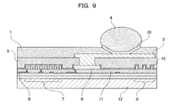
- FIG. 9 is a cross-sectional view of substantial parts showing the configuration of a semiconductor device according to a fourth embodiment.
- FIG. 10 is a cross-sectional diagram of substantial parts showing the configuration of a conventional semiconductor device and a corresponding wiring layout view
- FIG. 11 is a diagram showing a mounted state of a conventional WLCSP
- FIG. 12 is an enlarged view of substantial parts showing the mounted state of the conventional WLCSP.
- FIG. 13 is a diagram showing a load applied in the vicinity of semiconductor wiring and a stress concentration site during mounting of the conventional WLCSP.
- FIG. 1 is a cross-sectional diagram of substantial parts showing the configuration of a semiconductor device according to the present invention.
- FIG. 2 is a cross-sectional diagram of substantial parts showing the configuration of the semiconductor device and a corresponding wiring layout plan view.
- FIG. 3 is a diagram illustrating, within a WLCSP, a signal wiring disposition forbidden region in the semiconductor device according to the present invention.
- FIG. 4 is a diagram illustrating the proximity of the edge face of the WLCSP in the signal wiring disposition forbidden region in the semiconductor device according to the present invention;
- FIG. 5 is a diagram illustrating the signal wiring disposition forbidden region in the semiconductor device according to the present invention.
- FIG. 6 is a diagram showing the configuration of signal wiring in a signal wiring disposition forbidden region according to a first embodiment.
- FIG. 1 is a cross-sectional diagram of substantial parts showing the configuration of a semiconductor device according to the present invention.
- FIG. 2 is a cross-sectional diagram of substantial parts showing the configuration of the semiconductor device and a corresponding wiring layout plan
- FIG. 7 is a diagram showing the configuration of signal wiring of a signal wiring disposition forbidden region according to a second embodiment.
- FIG. 8 is a diagram showing the configuration of signal wiring in a signal wiring disposition forbidden region according to a third embodiment.
- FIG. 9 is a cross-sectional view of substantial parts showing the configuration of a semiconductor device according to a fourth embodiment.
- reference numeral 1 denotes a molding resin, 2 a post, 3 rewiring, 4 a solder bump having a circular planar shape, 5 an insulating film, 6 an Al wiring pad, 7 an Al wiring inductor, 8 first signal wiring, 9 second signal wiring, 10 a surface protective film, 11 an interlayer insulating film, 12 a semiconductor substrate, 15 a WLCSP lateral face in the vicinity of a formation region of the solder bump 4 of the WLCSP having a surface on which the solder bump 4 is formed, 16 a signal wiring disposition forbidden region, and 20 a UBM (underbump metal film).
- the second signal wiring 9 actual wiring through which electric signals pass is denoted by wiring 9 b while dummy wiring through which electric signals do not pass is denoted by wiring 9 a and 9 c.
- a semiconductor element such as an MOS transistor and a semiconductor element such as a diode and a bipolar transistor formed by a PN junction are formed on the semiconductor substrate 12 .
- the semiconductor substrate 12 is covered by the interlayer insulating film 11 to protect the semiconductor elements.
- Also disposed on the semiconductor substrate are; the first signal wiring 8 for conducting a signal from the semiconductor element; the second signal wiring 9 provided on the first signal wiring 8 and which is electrically insulated by the interlayer insulating film 11 using a multilayer wiring technique; the Al wiring inductor 7 ; and the Al wiring pad 6 for extracting signals to the outside.
- the wiring material of the second signal wiring 9 desirably includes Al, and in consideration of inductor characteristics, wiring having a thick film thickness of about 1.5 ⁇ m or more is used for the second signal wiring 9 , the Al wiring pad 6 and the Al wiring inductor 7 .
- the surface protective film 10 is thinly formed with respect to the second signal wiring 9 .
- solder bump 4 and the rewiring 3 are connected via the post 2 for increased mounting reliability.
- the post 2 and the rewiring 3 are protected from external impact and the atmosphere by the molding resin 1 .
- the solder bump 4 to become a contact that connects to a mounting substrate is formed on the post 2 .
- the second signal wiring 9 is disposed directly beneath the outer peripheral section of the post 2 .
- the signal wiring 9 b is used for actually transmitting signals.
- the signal wiring 9 a and 9 c is dummy wiring which is not used for signal transmission.
- FIG. 3 is a diagram for illustrating which portion of the WLCSP the signal wiring disposition forbidden region 16 corresponds to.
- FIG. 3A is a perspective view of the entire WLCSP as seen from a solder bump formation plane;
- FIG. 3B is a drawing showing the WLCSP lateral face portion 15 and the centers of peripheral terminals;
- FIG. 3C is a drawing showing the signal wiring disposition forbidden region 16 constituted by the WLCSP lateral face portion 15 and the centers of the peripheral terminals;
- FIG. 4 is a diagram illustrating, as an enlargement of FIG. 3 , a half of the post 2 on a side proximal to the edge of the WLCSP with respect to the signal wiring disposition forbidden region 16 .
- a region between a line connecting the centers of terminals of the outermost periphery of the WLCSP and the WLCSP lateral face 15 is set as the signal wiring disposition forbidden region 16 within the WLCSP.
- the signal wiring disposition forbidden region 16 is positioned from the WLCSP lateral face 15 to the center of the post 2 .
- FIG. 5 is a diagram illustrating a case where a range of the signal wiring disposition forbidden region 16 is further limited and, in order to do so, the post 2 has been extracted.
- a perpendicular line is drawn from the WLCSP lateral face 15 to the center point of a planar circle (hereinafter referred to as a planar circle center) on a plane parallel to the semiconductor substrate of the solder bump 4 or, i.e., post 2 .
- a portion at which a fan-shaped region whose center point is the center of the planar circle of the solder bump 4 and which is spread at 70 degrees to the left and to the right from the perpendicular line overlaps with a region whose radius from the planar circle center is 4/5 to 6/5 the radius of the solder bump 4 is assumed to be the signal wiring disposition forbidden region 16 .
- the present invention is capable of suppressing occurrences of cracks in a surface protective film used in actual operations without imposing a change in external shape or inducing additional processes or costs.
- the spacing between the actual wiring and the dummy wiring is desirably set so as to be equal to or greater than the wiring width.
- the spacing is set equal to or greater than 2.0 ⁇ m when the wiring width is 2.0 ⁇ m.
- FIG. 6 is a diagram showing the first embodiment.
- Second signal wiring 9 is disposed in a signal wiring disposition forbidden region 16 in the vicinity of a WLCSP lateral face 15 of a post 2 .
- actual wiring through which electric signals pass is denoted by wiring 9 b while dummy wiring through which electric signals do not pass is denoted by wiring 9 a and 9 c .
- a stress generated in a heat treatment process during mounting of the WLCSP is dispersed to the second signal wiring 9 a and 9 c , in addition to the second signal wiring 9 b , thereby reducing a stress generated independently at the second signal wiring 9 b .
- a stress is uniformly generated across the entirety of the second signal wiring 9 , preventing occurrences of cracks in a surface protective film 10 and enabling a semiconductor device with superior reliability to be provided.
- FIG. 7 is a diagram showing the second embodiment.
- Second signal wiring 9 is disposed in a signal wiring disposition forbidden region 16 in the vicinity of a WLCSP lateral face 15 of a post 2 .
- actual wiring through which electric signals pass is denoted by wiring 9 b while dummy wiring through which electric signals do not pass is denoted by wiring 9 a .
- a stress generated in a heat treatment process during mounting of the WLCSP is dispersed to the second signal wiring 9 a , in addition to the second signal wiring 9 b , thereby reducing a stress generated independently at the second signal wiring 9 b .
- a stress is uniformly generated across the entirety of the second signal wiring 9 , preventing occurrences of cracks in a surface protective film 10 and enabling a semiconductor device with superior reliability to be provided.
- FIG. 8 is a diagram showing the third embodiment.
- Second signal wiring 9 is disposed in a signal wiring disposition forbidden region 16 in the vicinity of a WLCSP lateral face 15 of a post 2 .
- a wiring width of 10 ⁇ m or more is secured for the second signal wiring 9 through which electric signals pass and which is to be used in actual operations. Due to the wiring width being 10 ⁇ m or more, a stress generated in a heat treatment process during mounting of the WLCSP is dispersed across the 10 ⁇ m-width of the second signal wiring 9 compared to a case where the second signal wiring 9 has a typical width of 2 ⁇ m. As a result, a stress is uniformly generated across the entirety of the second signal wiring 9 , preventing occurrences of cracks in a surface protective film 10 and enabling a semiconductor device with superior reliability to be provided.
- FIG. 9 is a diagram showing the fourth embodiment. Components similar to those in FIG. 1 are represented by the same reference characters and the description of the components will be omitted.
- a WLCSP according to the fourth embodiment is a form not including a post 2 and, in contrast to the WLCSP described above, a solder bump 4 is directly formed on a UBM 20 on rewiring 3 instead of on the post 2 .
- a stress generated in a heat treatment process during mounting of the WLCSP is dispersed by providing dummy wiring 9 a or dummy wiring 9 c or by securing a wiring width of 10 ⁇ m or more for second signal wiring 9 through which electric signals pass and which is to be used in actual operations as was the case with the first to third embodiments.
- occurrences of cracks in a surface protective film 10 can be suppressed and a semiconductor device with superior reliability can be provided.
- a portion overlapping a region whose radius from the planar center is 4/5 to 6/5 the radius of the solder bump can be set to a range enclosed by an arc whose center is the centroid of an external terminal and whose radius is 4/5 of a minimum distance to the edge of the external terminal and an arc whose center is the centroid of the external terminal and whose radius is 6/5 of a maximum distance to the edge of the external terminal.
Landscapes
- Internal Circuitry In Semiconductor Integrated Circuit Devices (AREA)
- Semiconductor Integrated Circuits (AREA)
Abstract
Description
Claims (32)
Applications Claiming Priority (4)
| Application Number | Priority Date | Filing Date | Title |
|---|---|---|---|
| JP2007-265973 | 2007-10-12 | ||
| JP2007265973 | 2007-10-12 | ||
| JP2008133712A JP2009111333A (en) | 2007-10-12 | 2008-05-22 | Semiconductor device |
| JP2008-133712 | 2008-05-22 |
Publications (2)
| Publication Number | Publication Date |
|---|---|
| US20090096094A1 US20090096094A1 (en) | 2009-04-16 |
| US8084859B2 true US8084859B2 (en) | 2011-12-27 |
Family
ID=40533388
Family Applications (1)
| Application Number | Title | Priority Date | Filing Date |
|---|---|---|---|
| US12/207,790 Active 2029-05-16 US8084859B2 (en) | 2007-10-12 | 2008-09-10 | Semiconductor device |
Country Status (1)
| Country | Link |
|---|---|
| US (1) | US8084859B2 (en) |
Cited By (4)
| Publication number | Priority date | Publication date | Assignee | Title |
|---|---|---|---|---|
| US20110241816A1 (en) * | 2010-04-05 | 2011-10-06 | Samsung Electro-Mechanics Co., Ltd. | Planar transformer and method of manufacturing the same |
| US8680647B2 (en) | 2011-12-29 | 2014-03-25 | Taiwan Semiconductor Manufacturing Company, Ltd. | Packages with passive devices and methods of forming the same |
| US8809996B2 (en) * | 2012-06-29 | 2014-08-19 | Taiwan Semiconductor Manufacturing Company, Ltd. | Package with passive devices and method of forming the same |
| US11049827B2 (en) | 2019-08-09 | 2021-06-29 | Samsung Electronics Co., Ltd. | Semiconductor devices including a thick metal layer and a bump |
Families Citing this family (9)
| Publication number | Priority date | Publication date | Assignee | Title |
|---|---|---|---|---|
| US8227926B2 (en) | 2009-10-23 | 2012-07-24 | Ati Technologies Ulc | Routing layer for mitigating stress in a semiconductor die |
| US8299632B2 (en) * | 2009-10-23 | 2012-10-30 | Ati Technologies Ulc | Routing layer for mitigating stress in a semiconductor die |
| JP5544872B2 (en) * | 2009-12-25 | 2014-07-09 | 富士通セミコンダクター株式会社 | Semiconductor device and manufacturing method thereof |
| US9355979B2 (en) * | 2013-08-16 | 2016-05-31 | Taiwan Semiconductor Manufacturing Company, Ltd. | Alignment structures and methods of forming same |
| US9570430B2 (en) * | 2014-05-13 | 2017-02-14 | GlobalFoundries, Inc. | Articles including bonded metal structures and methods of preparing the same |
| CN110610917B (en) * | 2019-10-23 | 2024-08-02 | 普冉半导体(上海)股份有限公司 | Chip structure of wafer level chip scale package |
| KR102902631B1 (en) * | 2021-01-29 | 2025-12-22 | 삼성전자주식회사 | Semiconductor package including a post |
| US12191342B2 (en) * | 2021-02-09 | 2025-01-07 | Mediatek Inc. | Asymmetric 8-shaped inductor and corresponding switched capacitor array |
| US12205889B2 (en) * | 2021-08-31 | 2025-01-21 | Taiwan Semiconductor Manufacturing Company, Ltd. | Semiconductor device and method of fabricating the same |
Citations (3)
| Publication number | Priority date | Publication date | Assignee | Title |
|---|---|---|---|---|
| JPH07273292A (en) | 1994-03-31 | 1995-10-20 | Matsushita Electron Corp | Semiconductor integrated circuit |
| US5539551A (en) * | 1992-12-28 | 1996-07-23 | Casio Computer Co., Ltd. | LCD TFT drain and source electrodes having ohmic barrier, primary conductor, and liquid impermeable layers and method of making |
| US20020140083A1 (en) * | 2001-03-27 | 2002-10-03 | Nec Corporation | Semiconductor device haivng resin-sealed area on circuit board thereof |
-
2008
- 2008-09-10 US US12/207,790 patent/US8084859B2/en active Active
Patent Citations (3)
| Publication number | Priority date | Publication date | Assignee | Title |
|---|---|---|---|---|
| US5539551A (en) * | 1992-12-28 | 1996-07-23 | Casio Computer Co., Ltd. | LCD TFT drain and source electrodes having ohmic barrier, primary conductor, and liquid impermeable layers and method of making |
| JPH07273292A (en) | 1994-03-31 | 1995-10-20 | Matsushita Electron Corp | Semiconductor integrated circuit |
| US20020140083A1 (en) * | 2001-03-27 | 2002-10-03 | Nec Corporation | Semiconductor device haivng resin-sealed area on circuit board thereof |
Cited By (13)
| Publication number | Priority date | Publication date | Assignee | Title |
|---|---|---|---|---|
| US8502633B2 (en) * | 2010-04-05 | 2013-08-06 | Samsung Electro-Mechanics Co., Ltd. | Planar transformer and method of manufacturing the same |
| US20110241816A1 (en) * | 2010-04-05 | 2011-10-06 | Samsung Electro-Mechanics Co., Ltd. | Planar transformer and method of manufacturing the same |
| US9040381B2 (en) | 2011-12-29 | 2015-05-26 | Taiwan Semiconductor Manufacturing Company, Ltd. | Packages with passive devices and methods of forming the same |
| US8680647B2 (en) | 2011-12-29 | 2014-03-25 | Taiwan Semiconductor Manufacturing Company, Ltd. | Packages with passive devices and methods of forming the same |
| US10373923B2 (en) | 2012-06-29 | 2019-08-06 | Taiwan Semiconductor Manufacturing Company, Ltd. | Package with passive devices and method of forming the same |
| US9831200B2 (en) | 2012-06-29 | 2017-11-28 | Taiwan Semiconductor Manufacturing Company, Ltd. | Package with passive devices and method of forming the same |
| US8809996B2 (en) * | 2012-06-29 | 2014-08-19 | Taiwan Semiconductor Manufacturing Company, Ltd. | Package with passive devices and method of forming the same |
| US10700032B2 (en) | 2012-06-29 | 2020-06-30 | Taiwan Semiconductor Manufacturing Company, Ltd. | Package with passive devices and method of forming the same |
| US11004818B2 (en) | 2012-06-29 | 2021-05-11 | Taiwan Semiconductor Manufacturing Company, Ltd. | Package with passive devices and method of forming the same |
| US11049827B2 (en) | 2019-08-09 | 2021-06-29 | Samsung Electronics Co., Ltd. | Semiconductor devices including a thick metal layer and a bump |
| US11557556B2 (en) | 2019-08-09 | 2023-01-17 | Samsung Electronics Co., Ltd. | Semiconductor devices including a thick metal layer and a bump |
| US11817408B2 (en) | 2019-08-09 | 2023-11-14 | Samsung Electronics Co., Ltd. | Semiconductor devices including a thick metal layer and a bump |
| US12080663B2 (en) | 2019-08-09 | 2024-09-03 | Samsung Electronics Co., Ltd. | Semiconductor devices including a thick metal layer and a bump |
Also Published As
| Publication number | Publication date |
|---|---|
| US20090096094A1 (en) | 2009-04-16 |
Similar Documents
| Publication | Publication Date | Title |
|---|---|---|
| US8084859B2 (en) | Semiconductor device | |
| JP5617980B2 (en) | ESD protection device | |
| US9607967B1 (en) | Multi-chip semiconductor package with via components and method for manufacturing the same | |
| US10020298B2 (en) | ESD protection device | |
| JP6180801B2 (en) | Semiconductor device | |
| US20170271286A1 (en) | Semiconductor device capable of dispersing stresses | |
| US9859187B2 (en) | Ball grid array package with protective circuitry layout and a substrate utilized in the package | |
| JP4776861B2 (en) | Semiconductor device | |
| US8098496B2 (en) | Wiring board for semiconductor device | |
| CN112117262B (en) | Semiconductor package | |
| US20240413036A1 (en) | Semiconductor device and semiconductor module | |
| JP2009111333A (en) | Semiconductor device | |
| US7323779B2 (en) | Semiconductor device | |
| US11817493B2 (en) | Semiconductor device | |
| TW201604965A (en) | Semiconductor component and high frequency amplifier module | |
| JP4658914B2 (en) | Semiconductor device and manufacturing method thereof | |
| JP2012015468A (en) | Semiconductor device | |
| TW200527616A (en) | Stacked type semiconductor encapsulation device having protection mask | |
| JP2010263234A (en) | Semiconductor integrated circuit device | |
| KR20120018599A (en) | Memory card and method of manufacture the same |
Legal Events
| Date | Code | Title | Description |
|---|---|---|---|
| AS | Assignment |
Owner name: PANASONIC CORPORATION, JAPAN Free format text: ASSIGNMENT OF ASSIGNORS INTEREST;ASSIGNORS:TETANI, MICHINARI;FUJISAKU, MINORU;REEL/FRAME:021689/0493 Effective date: 20080904 |
|
| FEPP | Fee payment procedure |
Free format text: PAYOR NUMBER ASSIGNED (ORIGINAL EVENT CODE: ASPN); ENTITY STATUS OF PATENT OWNER: LARGE ENTITY |
|
| STCF | Information on status: patent grant |
Free format text: PATENTED CASE |
|
| FPAY | Fee payment |
Year of fee payment: 4 |
|
| MAFP | Maintenance fee payment |
Free format text: PAYMENT OF MAINTENANCE FEE, 8TH YEAR, LARGE ENTITY (ORIGINAL EVENT CODE: M1552); ENTITY STATUS OF PATENT OWNER: LARGE ENTITY Year of fee payment: 8 |
|
| AS | Assignment |
Owner name: PANASONIC SEMICONDUCTOR SOLUTIONS CO., LTD., JAPAN Free format text: ASSIGNMENT OF ASSIGNORS INTEREST;ASSIGNOR:PANASONIC CORPORATION;REEL/FRAME:052755/0917 Effective date: 20200521 |
|
| MAFP | Maintenance fee payment |
Free format text: PAYMENT OF MAINTENANCE FEE, 12TH YEAR, LARGE ENTITY (ORIGINAL EVENT CODE: M1553); ENTITY STATUS OF PATENT OWNER: LARGE ENTITY Year of fee payment: 12 |