US8081941B2 - Method and system for RF front-end calibration scheme using fractional-N frequency synthesized signals and RSSI - Google Patents
Method and system for RF front-end calibration scheme using fractional-N frequency synthesized signals and RSSI Download PDFInfo
- Publication number
- US8081941B2 US8081941B2 US12/709,974 US70997410A US8081941B2 US 8081941 B2 US8081941 B2 US 8081941B2 US 70997410 A US70997410 A US 70997410A US 8081941 B2 US8081941 B2 US 8081941B2
- Authority
- US
- United States
- Prior art keywords
- lna
- signal
- tunable
- communicatively coupled
- generated
- Prior art date
- Legal status (The legal status is an assumption and is not a legal conclusion. Google has not performed a legal analysis and makes no representation as to the accuracy of the status listed.)
- Expired - Fee Related
Links
- 238000000034 method Methods 0.000 title claims abstract description 39
- 239000003990 capacitor Substances 0.000 claims description 13
- 238000004590 computer program Methods 0.000 claims description 4
- 230000008569 process Effects 0.000 abstract description 17
- 238000006243 chemical reaction Methods 0.000 description 26
- 238000010586 diagram Methods 0.000 description 22
- 238000012545 processing Methods 0.000 description 18
- 230000005540 biological transmission Effects 0.000 description 11
- 230000003321 amplification Effects 0.000 description 10
- 238000005259 measurement Methods 0.000 description 10
- 238000003199 nucleic acid amplification method Methods 0.000 description 10
- 239000013078 crystal Substances 0.000 description 9
- 229920000954 Polyglycolide Polymers 0.000 description 8
- 235000010409 propane-1,2-diol alginate Nutrition 0.000 description 8
- 230000001413 cellular effect Effects 0.000 description 7
- 238000004891 communication Methods 0.000 description 7
- 238000005516 engineering process Methods 0.000 description 5
- 238000001914 filtration Methods 0.000 description 5
- 230000006870 function Effects 0.000 description 4
- 238000010295 mobile communication Methods 0.000 description 4
- 238000005070 sampling Methods 0.000 description 4
- 230000006978 adaptation Effects 0.000 description 3
- 238000013459 approach Methods 0.000 description 3
- 230000008901 benefit Effects 0.000 description 3
- 230000000694 effects Effects 0.000 description 3
- 239000004065 semiconductor Substances 0.000 description 3
- 238000000926 separation method Methods 0.000 description 3
- 229910000577 Silicon-germanium Inorganic materials 0.000 description 2
- 230000015572 biosynthetic process Effects 0.000 description 2
- 230000000903 blocking effect Effects 0.000 description 2
- 238000012937 correction Methods 0.000 description 2
- 238000013461 design Methods 0.000 description 2
- 238000011161 development Methods 0.000 description 2
- 230000018109 developmental process Effects 0.000 description 2
- 239000000463 material Substances 0.000 description 2
- 238000001228 spectrum Methods 0.000 description 2
- 238000003786 synthesis reaction Methods 0.000 description 2
- 238000012546 transfer Methods 0.000 description 2
- LEVVHYCKPQWKOP-UHFFFAOYSA-N [Si].[Ge] Chemical compound [Si].[Ge] LEVVHYCKPQWKOP-UHFFFAOYSA-N 0.000 description 1
- 238000009825 accumulation Methods 0.000 description 1
- 230000002238 attenuated effect Effects 0.000 description 1
- 230000006399 behavior Effects 0.000 description 1
- 239000000969 carrier Substances 0.000 description 1
- 230000010267 cellular communication Effects 0.000 description 1
- 230000008878 coupling Effects 0.000 description 1
- 238000010168 coupling process Methods 0.000 description 1
- 238000005859 coupling reaction Methods 0.000 description 1
- 238000009826 distribution Methods 0.000 description 1
- 238000010348 incorporation Methods 0.000 description 1
- 230000001939 inductive effect Effects 0.000 description 1
- 230000010365 information processing Effects 0.000 description 1
- 230000002452 interceptive effect Effects 0.000 description 1
- 238000004519 manufacturing process Methods 0.000 description 1
- 230000007246 mechanism Effects 0.000 description 1
- 238000012986 modification Methods 0.000 description 1
- 230000004048 modification Effects 0.000 description 1
- 238000005457 optimization Methods 0.000 description 1
- 230000004044 response Effects 0.000 description 1
- 230000003595 spectral effect Effects 0.000 description 1
- 230000003068 static effect Effects 0.000 description 1
- 238000003860 storage Methods 0.000 description 1
- 239000000758 substrate Substances 0.000 description 1
Images


Classifications
-
- H—ELECTRICITY
- H04—ELECTRIC COMMUNICATION TECHNIQUE
- H04B—TRANSMISSION
- H04B17/00—Monitoring; Testing
- H04B17/20—Monitoring; Testing of receivers
- H04B17/21—Monitoring; Testing of receivers for calibration; for correcting measurements
-
- H—ELECTRICITY
- H04—ELECTRIC COMMUNICATION TECHNIQUE
- H04B—TRANSMISSION
- H04B7/00—Radio transmission systems, i.e. using radiation field
- H04B7/02—Diversity systems; Multi-antenna system, i.e. transmission or reception using multiple antennas
- H04B7/04—Diversity systems; Multi-antenna system, i.e. transmission or reception using multiple antennas using two or more spaced independent antennas
- H04B7/08—Diversity systems; Multi-antenna system, i.e. transmission or reception using multiple antennas using two or more spaced independent antennas at the receiving station
-
- H—ELECTRICITY
- H04—ELECTRIC COMMUNICATION TECHNIQUE
- H04H—BROADCAST COMMUNICATION
- H04H60/00—Arrangements for broadcast applications with a direct linking to broadcast information or broadcast space-time; Broadcast-related systems
- H04H60/76—Arrangements characterised by transmission systems other than for broadcast, e.g. the Internet
- H04H60/81—Arrangements characterised by transmission systems other than for broadcast, e.g. the Internet characterised by the transmission system itself
- H04H60/90—Wireless transmission systems
- H04H60/91—Mobile communication networks
Definitions
- Certain embodiments of the invention relate to on-chip RF tuners. More specifically, certain embodiments of the invention relate to a method and system for an RF front-end calibration scheme using signals from a fractional-N frequency synthesizer and a received signal strength indicator (RSSI).
- RSSI received signal strength indicator
- Broadcasting and telecommunications have historically occupied separate fields.
- broadcasting was largely an “over-the-air” medium while wired media carried telecommunications. That distinction may no longer apply as both broadcasting and telecommunications may be delivered over either wired or wireless media.
- Present development may adapt broadcasting to mobility services.
- One limitation has been that broadcasting may often require high bit rate data transmission at rates higher than could be supported by existing mobile communications networks.
- wireless communications technology even this obstacle may be overcome.
- Terrestrial television and radio broadcast networks have made use of high power transmitters covering broad service areas, which enable one-way distribution of content to user equipment such as televisions and radios.
- wireless telecommunications networks have made use of low power transmitters, which have covered relatively small areas known as “cells”.
- wireless networks may be adapted to provide two-way interactive services between users of user equipment such as telephones and computer equipment.
- first generation systems The networks of this period may be commonly known as first generation, or “1G” systems. These systems were based upon analog, circuit-switching technology, the most prominent of these systems may have been the advanced mobile phone system (AMPS). Second generation, or “2G” systems ushered improvements in performance over 1G systems and introduced digital technology to mobile communications. Exemplary 2G systems include the global system for mobile communications (GSM), digital AMPS (D-AMPS), and code division multiple access (CDMA). Many of these systems have been designed according to the paradigm of the traditional telephony architecture, often focused on circuit-switched services, voice traffic, and supported data transfer rates up to 14.4 kbits/s.
- GSM global system for mobile communications
- D-AMPS digital AMPS
- CDMA code division multiple access
- the 2.5G networks began the introduction of packet-switching technology in wireless networks. However, it is the evolution of third generation, or “3G” technology that may introduce fully packet-switched networks, which support high-speed data communications.
- DTTB Digital television terrestrial broadcasting
- ATSC advanced standards technical committee
- DVD-T digital video broadcast terrestrial
- ISDB-T integrated service digital broadcasting terrestrial
- the ATSC system has largely been adopted in North America, South America, Taiwan, and South Korea.
- This system adapts trellis coding and 8-level vestigial sideband (8-VSB) modulation.
- the DVB-T system has largely been adopted in Europe, the Middle East, Australia, as well as parts of Africa and parts of Asia.
- the DVB-T system adapts coded orthogonal frequency division multiplexing (COFDM).
- COFDM coded orthogonal frequency division multiplexing
- the OFDM spread spectrum technique may be utilized to distribute information over many carriers that are spaced apart at specified frequencies.
- the OFDM technique may also be referred to as multi-carrier or discrete multi-tone modulation. This technique may result in spectral efficiency and lower multi-path distortion, for example.
- the ISDB-T system has been adopted in Japan and adapts bandwidth segmented transmission orthogonal frequency division multiplexing (BST-OFDM).
- BST-OFDM bandwidth segmented transmission orthogonal frequency division multiplexing
- the various DTTB systems may differ in important aspects; some systems employ a 6 MHz channel separation, while others may employ 7 MHz or 8 MHz channel separations.
- DVB-T may support data rates of 15 Mbits/s in an 8 MHz channel in a wide area single frequency network (SFN).
- SFN wide area single frequency network
- ISDB-T was originally designed to support broadcast services to mobile user equipment. While DVB-T may not have been originally designed to support mobility broadcast services, a number of adaptations have been made to provide support for mobile broadcast capability.
- the adaptation of DVB-T to mobile broadcasting is commonly known as DVB handheld (DVB-H).
- the broadcasting frequencies for Europe are in UHF (bands IV/V) and in the US, the 1670-1675 MHz band that has been allocated for DVB-H operation. Additional spectrum is expected to be allocated in the L-band world-wide. Broadcasting frequencies for VHF channels may range between 174-240 MHZ, for example.
- DVB-H may also use the DVB-T modulation schemes, like QPSK and 16-quadrature amplitude modulation (16-QAM).
- DVB-T tuners or receivers in mobile terminals may employ super-heterodyne architectures with one or two intermediate frequency (IF) stages and direct sampling of the passband signal for digital quadrature down-conversion.
- IF intermediate frequency
- external tracking and SAW filters may generally be utilized for channel selection and image rejection.
- Such approaches may result in increased power consumption and high external component count, which may limit their application in handheld portable devices.
- the success of mobile broadcast capability of DVB-T may depend in part on the ability to develop TV tuners that have smaller form factor, are produced at lower cost, and consume less power during operation.
- LNAs low noise amplifiers
- the gain of the low noise amplifiers (LNAs), and other components of the receiver have to be very linear, that is, the output has to have a linear relationship with the input, to maintain the performance of the receiver.
- Blocker signals are unwanted signals in frequency channels outside the wanted channel that disturb the reception of the wanted signals. This happens due to the fact that the blockers generate large signals within the receiver path. These large signals may introduce harmonics and intermodulation products or unwanted mixing products that causes crosstalk with the wanted signals.
- NF noise factor
- the increased power consumption may significantly drain the battery that powers these devices.
- the gain in the LNA may be different for the wanted channel and for the blocker or interference signal.
- An LNA is usually “tuned” for a specific frequency range and may be difficult for the LNA to achieve optimal performance for a wide frequency range in the presence of blocker signals.
- the gain provided to the blocker signal may be larger than for the wanted channel when the LNA operates over a wide frequency range. This in turn further affects the harmonics and intermodulation products or unwanted mixing products that crosstalk with the wanted signals.
- Developing mechanisms that enable control of the LNA gain outside the wanted channel may be necessary in order to improve the performance of RF receivers in high bit rate data transmission applications, such as DVB-H applications, for example.
- a system and/or method is provided for an RF front-end calibration scheme using signals from a fractional-N frequency synthesizer and a received signal strength indicator (RSSI), substantially as shown in and/or described in connection with at least one of the figures, as set forth more completely in the claims.
- RSSI received signal strength indicator
- FIG. 1A is a block diagram illustrating an exemplary mobile terminal, accordance with an embodiment of the invention.
- FIG. 1B is a block diagram illustrating exemplary communication between a multi-band RF receiver and a digital baseband processor in a mobile terminal, in accordance with an embodiment of the invention.
- FIG. 1C is a block diagram illustrating an exemplary single-chip multi-band RF receiver with an integrated LNA in each front-end, in accordance with an embodiment of the invention.
- FIG. 1D is a block diagram illustrating an exemplary single-chip multi-band RF receiver with on-chip gain control processing, in accordance with an embodiment of the invention.
- FIG. 2 is a flow diagram illustrating exemplary steps in the operation of a single-chip multi-band RF receiver, in accordance with an embodiment of the invention.
- FIG. 3A is a diagram illustrating an exemplary fixed tuning curve for an integrated LNA in a multi-band RF receiver, in connection with an embodiment of the invention.
- FIG. 3B is a diagram illustrating an exemplary dynamically controlled tuning curve for an integrated LNA in a multi-band RF receiver, in accordance with an embodiment of the invention.
- FIG. 4 is a block diagram illustrating an exemplary system for dynamically controlling the LNA gain, in accordance with an embodiment of the invention.
- FIG. 5 is a schematic diagram illustrating an exemplary integrated LNA with tunable input load and tunable output load, in accordance with an embodiment of the invention.
- FIGS. 6A and 6B are flow diagrams illustrating exemplary steps in the calibration of a dynamically controlled variable gain LNA for a selected desired channel, in accordance with an embodiment of the invention.
- Certain embodiments of the invention may be found in a method and system for an RF front-end calibration scheme using fractional-N frequency synthesized signals and a received signal strength indicator (RSSI).
- RSSI received signal strength indicator
- aspects of the invention may comprise a frequency synthesizer within a wireless receiver that may generate a signal that may be utilized to dynamically modify a gain in an integrated low-noise amplifier (LNA) for each selected receiver channel.
- the frequency-synthesized signals may be applied to at least one tunable input and/or at least one tunable output load communicatively coupled to the LNA.
- the signal generated by the frequency synthesizer may be sequentially applied to the tunable input load and the tunable output load.
- a logarithmic amplifier connected to the output of the LNA may generate an RSSI signal during the calibration process, which is proportional to the signal power at the output of the LNA.
- the RSSI signal may be processed by a control block that subsequently generates at least one signal for controlling a tunable load communicatively coupled to the LNA.
- FIG. 1A is a block diagram illustrating an exemplary mobile terminal, in accordance with an embodiment of the invention.
- a mobile terminal 120 may comprise an RF receiver 123 a , an RF transmitter 123 b , a digital baseband processor 129 , a processor 125 , and a memory 127 .
- a receive antenna 121 a may be communicatively coupled to the RF receiver 123 a .
- a transmit antenna 121 b may be communicatively coupled to the RF transmitter 123 b .
- the mobile terminal 120 may be operated in a system, such as the cellular network and/or digital video broadcast network, for example.
- the U.S. application Ser. No. 11/385,390 filed on Mar. 21, 2006 discloses a cellular network and/or digital video broadcast network in reference to a method and system for a multi-band direct conversion CMOS mobile cellular television tuner, and is hereby incorporated herein by reference in its entirety.
- the RF receiver 123 a may comprise suitable logic, circuitry, and/or code that may enable processing of received RF signals.
- the RF receiver 123 a may enable receiving RF signals in a plurality of frequency bands.
- the RF receiver 123 a may enable receiving DVB-H transmission signals via the UHF band, from about 470 MHz to about 890 MHz, the 1670-1675 MHz band, and/or the L-band, from about 1400 MHz to about 1700 MHz, for example.
- the RF receiver 123 a may enable receiving signals in cellular frequency bands, for example.
- Each frequency band supported by the RF receiver 123 a may have a corresponding front-end circuit for handling low noise amplification and down conversion operations, for example.
- the RF receiver 123 a may be referred to as a multi-band receiver when it supports more than one frequency band.
- the mobile terminal 120 may comprise more than one RF receiver 123 a , wherein each of the RF receiver 123 a may be a single-band or a multi-band receiver.
- the RF receiver 123 a may quadrature down convert the received RF signal to a baseband frequency signal that comprises an in-phase (I) component and a quadrature (Q) component.
- the RF receiver 123 a may perform direct down conversion of the received RF signal to a baseband frequency signal, for example.
- the RF receiver 123 a may enable analog-to-digital conversion of the baseband signal components before transferring the components to the digital baseband processor 129 .
- the RF receiver 123 a may transfer the baseband signal components in analog form.
- the digital baseband processor 129 may comprise suitable logic, circuitry, and/or code that may enable processing and/or handling of baseband frequency signals.
- the digital baseband processor 129 may process or handle signals received from the RF receiver 123 a and/or signals to be transferred to the RF transmitter 123 b , when the RF transmitter 123 b is present, for transmission to the network.
- the digital baseband processor 129 may also provide control and/or feedback information to the RF receiver 123 a and to the RF transmitter 123 b based on information from the processed signals.
- the digital baseband processor 129 may communicate information and/or data from the processed signals to the processor 125 and/or to the memory 127 .
- the digital baseband processor 129 may receive information from the processor 125 and/or to the memory 127 , which may be processed and transferred to the RF transmitter 123 b for transmission to the network.
- the RF transmitter 123 b may comprise suitable logic, circuitry, and/or code that may enable processing of RF signals for transmission.
- the RF transmitter 123 b may enable transmission of RF signals in a plurality of frequency bands.
- the RF transmitter 123 b may enable transmitting signals in cellular frequency bands, for example.
- Each frequency band supported by the RF transmitter 123 b may have a corresponding front-end circuit for handling amplification and up conversion operations, for example.
- the RF transmitter 123 b may be referred to as a multi-band transmitter when it supports more than one frequency band.
- the mobile terminal 120 may comprise more than one RF transmitter 123 b , wherein each of the RF transmitter 123 b may be a single-band or a multi-band transmitter.
- the RF transmitter 123 b may quadrature up convert the baseband frequency signal comprising I/Q components to an RF signal.
- the RF transmitter 123 b may perform direct up conversion of the baseband frequency signal to a baseband frequency signal, for example.
- the RF transmitter 123 b may enable digital-to-analog conversion of the baseband signal components received from the digital baseband processor 129 before up conversion.
- the RF transmitter 123 b may receive baseband signal components in analog form.
- the processor 125 may comprise suitable logic, circuitry, and/or code that may enable control and/or data processing operations for the mobile terminal 120 .
- the processor 125 may be utilized to control at least a portion of the RF receiver 123 a , the RF transmitter 123 b , the digital baseband processor 129 , and/or the memory 127 .
- the processor 125 may generate at least one signal for controlling operations within the mobile terminal 120 .
- the processor 125 may also enable executing of applications that may be utilized by the mobile terminal 120 .
- the processor 125 may execute applications that may enable displaying and/or interacting with content received via DVB-H transmission signals in the mobile terminal 120 .
- the memory 127 may comprise suitable logic, circuitry, and/or code that may enable storage of data and/or other information utilized by the mobile terminal 120 .
- the memory 127 may be utilized for storing processed data generated by the digital baseband processor 129 and/or the processor 125 .
- the memory 127 may also be utilized to store information, such as configuration information, that may be utilized to control the operation of at least one block in the mobile terminal 120 .
- the memory 127 may comprise information necessary to configure the RF receiver 123 a to enable receiving DVB-H transmission in the appropriate frequency band.
- FIG. 1B is a block diagram illustrating exemplary communication between a multi-band RF receiver and a digital baseband processor in a mobile terminal, in accordance with an embodiment of the invention.
- a multi-band RF receiver 130 a multi-channel analog-to-digital converter (ADC) 134 , and a digital baseband processor 132 .
- the multi-band RF receiver 130 may comprise a UHF front-end 131 a , an L-band front-end 131 b , a VHF front-end 131 c , a baseband block 133 a , a received signal strength indicator (RSSI) block 133 b , and a synthesizer 133 c .
- the multi-band RF receiver 130 , the analog-to-digital converter (ADC) 134 , and/or the digital baseband processor 132 may be part of a mobile terminal, such as the mobile terminal 120 in FIG. 1A , for example.
- the multi-band RF receiver 130 may comprise suitable logic, circuitry, and/or code that may enable handling of UHF, VHF, and L-band signals.
- the multi-band RF receiver 130 may be enabled via an enable signal, such as the signal RxEN 139 a , for example.
- enabling the multi-band RF receiver 130 via the signal RxEN 139 a by a 1:10 ON/OFF ratio may allow time slicing in DVB-H while reducing power consumption.
- At least a portion of the circuitry within the multi-band RF receiver 130 may be controlled via the control interface 139 b .
- the control interface 139 b may receive information from, for example, a processor, such as the processor 125 in FIG. 1A , or from the digital baseband processor 132 .
- the control interface 139 b may comprise more than one bit.
- the control interface 139 a may be an inter-integrated circuit (I2C) interface.
- I2C inter-integrated circuit
- the UHF front-end 131 a may comprise suitable logic, circuitry, and/or code that may enable low noise amplification and direct down conversion of UHF signals.
- the UHF front-end 131 a may utilize an integrated low noise amplifier (LNA) and mixers, such as passive mixers, for example.
- LNA integrated low noise amplifier
- the UHF front-end 131 a may communicate the resulting baseband frequency signals to the baseband block 133 a for further processing.
- the L-band front-end 131 b may comprise suitable logic, circuitry, and/or code that may enable low noise amplification and direct down conversion of L-band signals.
- the L-band front-end 131 b may utilize an integrated LNA and mixers, such as passive mixers, for example.
- the L-band front-end 131 b may communicate the resulting baseband frequency signals to the baseband block 133 a for further processing.
- the VHF front-end 131 c may comprise suitable logic, circuitry, and/or code that may enable low noise amplification and direct down conversion of VHF signals.
- the VHF front-end 131 c may utilize an integrated low noise amplifier (LNA) and mixers, such as passive mixers, for example.
- LNA integrated low noise amplifier
- the VHF front-end 131 c may communicate the resulting baseband frequency signals to the baseband block 133 a for further processing.
- the multi-band RF receiver 130 may enable one of the UHF front-end 131 a , the L-band front-end 131 b , and the VHF front-end 131 c based on current communication conditions.
- the synthesizer 133 c may comprise suitable logic, circuitry, and/or code that may enable generating the appropriate local oscillator (LO) signal for performing direct down conversion in the UHF front-end 131 a , the L-band front-end 131 b , or the VHF front-end 131 c . Since the synthesizer 133 c may enable fractional multiplication of a source frequency when generating the LO signal, a large range of crystal oscillators may be utilized as a frequency source for the synthesizer 133 c . This approach may enable the use of an existing crystal oscillator in a mobile terminal PCB, thus reducing the number of external components necessary to support the operations of the multi-band RF receiver 130 , for example.
- LO local oscillator
- the synthesizer 133 may generate a common LO signal for the UHF front-end 131 a , the L-band front-end 131 b , and the VHF front-end 131 c .
- the UHF front-end 131 a , the L-band front-end 131 b , and the VHF front-end 131 c may enable dividing the LO signal in order to generate the appropriate signal to perform down conversion from the UHF band, the L-band, and the VHF band respectively.
- the synthesizer 133 may have at least one integrated voltage controlled oscillator (VCO) for generating the LO signal. In other instances, the VCO may be implemented outside the synthesizer 133 .
- VCO voltage controlled oscillator
- the baseband block 133 a may comprise suitable logic, circuitry, and/or code that may enable processing of I/Q components generated from the direct down conversion operations in the UHF front-end 131 a , L-band front-end 131 b , and the VHF front-end 131 c .
- the baseband block 133 a may enable amplification and/or filtering of the I/Q components in analog form.
- the baseband block 133 a may communicate the processed I component, that is, signal 135 a , and the processed Q component, that is, signal 135 c , to the multi-channel ADC 134 for digital conversion.
- the RSSI block 133 b may comprise suitable logic, circuitry, and/or code that may enable measuring the strength, that is, the RSSI value, of a received RF signal, whether UHF, L-band, or VHF signal.
- the RSSI block 133 b may be implemented based on a logarithmic amplifier, for example.
- the RSSI measurement may be performed, for example, after the received RF signal is amplified in the UHF front-end 131 a , the L-band front-end 131 b , or the VHF front-end 131 c .
- the RSSI block 133 b may communicate the analog RSSI measurement, that is, signal 135 e , to the multi-channel ADC 134 for digital conversion.
- the multi-channel ADC 134 may comprise suitable logic, circuitry, and/or code that may enable digital conversion of signals 135 a , 135 c , and/or 135 e to signals 135 b , 135 d , and/or 135 f respectively. In some instances, the multi-channel ADC 134 may be integrated into the multi-band RF receiver 130 or into the digital baseband processor 132 .
- the digital baseband processor 132 may comprise suitable logic, circuitry, and/or code that may enable processing and/or handling of baseband frequency signals.
- the digital baseband processor 132 may be the same or substantially similar to the digital baseband processor 129 described in FIG. 1A .
- the digital baseband processor 132 may enable generating at least one signal, such as the signals AGC_BB 137 a and AGC_RF 137 b , for adjusting the operations of the multi-band RF receiver 130 .
- the signal AGC_BB 137 a may be utilized to adjust the gain provided by the baseband block 133 a on the baseband frequency signals generated from the UHF front-end 131 a , the L-band front-end 131 b , or the VHF front-end 131 c .
- the signal AGC_RF 137 b may be utilized to adjust the gain provided by an integrated LNA in the UHF front-end 131 a , the L-band front-end 131 b , or the VHF front-end 131 c .
- the signal AGC_RF 137 b may be utilized to adjust the gain during a calibration mode, for example.
- the digital baseband processor 132 may generate at least one control signal or control information communicated to the multi-band RF receiver 130 via the control interface 139 b for adjusting operations within the multi-band RF receiver 130 .
- FIG. 1C is a block diagram illustrating an exemplary single-chip multi-band RF receiver with an integrated LNA in each front-end, in accordance with an embodiment of the invention.
- a single-chip multi-band RF receiver 140 a that may comprise a UHF front-end 148 a , an L-band front-end 148 b , a VHF front-end 148 c , a baseband block 164 , a logarithmic amplifier 172 , a digital frequency synthesizer 189 , a ⁇ - ⁇ fractional-N synthesizer 174 , a VCO block 176 , a digital interface 160 , an ADC 162 , an oscillator 180 , and a buffer 182 .
- the single-chip multi-band RF receiver 140 a may be fabricated using any of a plurality of semiconductor manufacturing processes, for example, complimentary metal-oxide-semiconductor (CMOS) processes, bipolar CMOS (BiCMOS), or Silicon Germanium (SiGe).
- CMOS complimentary metal-oxide-semiconductor
- BiCMOS bipolar CMOS
- SiGe Silicon Germanium
- the single-chip multi-band RF receiver 140 a may be implemented using differential structures to minimize noise effects and/or substrate coupling, for example.
- the single-chip multi-band RF receiver 140 a may utilize low drop out (LDO) voltage regulators to regulate and clean up on-chip voltage supplies.
- the LDO voltage regulators may be utilized to transform external voltage sources to the appropriate on-chip voltages.
- some design considerations may include achieving low noise figure (NF) values, wide-band operation, high signal-to-noise ration (SNR), performing DC offset removal, achieving high input second-order and third-order intercept points (IIP2 and IIP3), and/or reducing I/Q mismatch, for example.
- NF low noise figure
- SNR signal-to-noise ration
- IIP2 and IIP3 high input second-order and third-order intercept points
- I/Q mismatch for example.
- the single-chip multi-band RF receiver 140 a may receive UHF signals via a first antenna 142 a , a UHF filter 144 a , and a first balum 146 a .
- the UHF filter 144 a enables band pass filtering, wherein the band pass may be about 470 to about 702 MHz for cellular signals, for example, or about 470 to about 862 MHz, for other types of received signals, for example.
- the balum 146 a enables balancing the filtered signals before being communicated to the UHF front-end 148 a.
- the single-chip multi-band RF receiver 140 a may receive L-band signals via a second antenna 142 b , an L-band filter 144 b , and a second balum 146 b .
- the L-band filter 144 b enables band pass filtering, wherein the band pass may be about 1670 to about 1675 MHz for signals in US systems, for example, or about 1450 to about 1490 MHz, for signals in European systems, for example.
- the balum 146 b enables balancing the filtered signals before being communicated to the L-band front-end 148 a.
- the single-chip multi-band RF receiver 140 a may receive VHF signals via a third antenna 142 c , a VHF filter 144 c , and a third balum 146 c .
- the VHF filter 144 c enables band pass filtering, wherein the band pass may be about 174 to about 240 MHz for signals in US systems, for example.
- the balum 146 c enables balancing the filtered signals before being communicated to the VHF front-end 148 c .
- antennas 142 a , 142 b and 142 c may be implemented utilizing a single antenna communicatively coupled to the single-chip multi-band RF receiver 140 a that may support receiving radio signals operating in the UHF, L-band, and/or VHF frequencies, for example.
- the UHF front-end 148 a may comprise a variable gain low noise amplifier (LNA) 150 a , a mixer 152 a , a mixer 154 a , and a LO signal divider 156 a .
- the variable gain LNA 150 a may comprise suitable logic and/or circuitry that may enable amplification of the UHF signals received. Matching between the output of the balum 146 a and the input of the variable gain LNA 150 a may be achieved by utilizing off-chip series inductors, for example.
- the variable gain LNA 150 a may implement continuous gain control by current steering that may be controlled by a replica scheme within the variable gain LNA 150 a .
- the gain of the variable gain LNA 150 a may be adjusted via the signal AGC_RF 137 b , for example.
- the gain of the variable gain LNA 150 a may be adjusted during a calibration mode for each selected desired channel of operation within the frequency range provided by the UHF front-end 148 a , for example.
- the mixers 152 a and 154 a may comprise suitable logic and/or circuitry that may enable generating in-phase (I) and quadrature (Q) components of the baseband frequency signal based on direct down conversion of the amplified received UHF signal with the quadrature signals 186 I and 186 Q generated by the divider block 156 a .
- the mixers 152 a and 154 a may be passive mixers in order to achieve high linearity and/or low flicker noise, for example.
- the LO signal divider 156 a may comprise suitable logic, circuitry, and/or code that may enable dividing of the LO signal 186 by a factor of 2 (:/2) or a factor of 3 (:/3) and at the same time provide quadrature outputs 186 I and 186 Q, wherein 186 I and 186 Q have 90 degrees separation between them.
- the factor of 3 division may be used when the received UHF signal band is about 470 to about 600 MHz, for example.
- the factor of 2 division may be used when the received UHF signal band is about 600 to about 900 MHz, for example.
- the I/Q components generated by the mixers 152 a and 154 a may be communicated to the baseband block 164 .
- the L-band front-end 148 b may comprise a variable gain LNA 150 b , a mixer 152 a , a mixer 154 a , and a LO signal generator 158 .
- the variable gain LNA 150 a may comprise suitable logic and/or circuitry that may enable amplification of the L-band signals received. Matching between the output of the balum 146 b and the input of the variable gain LNA 150 b may be achieved by utilizing off-chip series inductors, for example.
- the variable gain LNA 150 b may implement continuous gain control by current steering that may be controlled by a replica scheme within the variable gain LNA 150 b .
- the gain of the variable gain LNA 150 b may be adjusted via the signal AGC_RF 137 b , for example. In this regard, the gain of the variable gain LNA 150 b may be adjusted during a calibration mode for each selected desired channel of operation within the frequency range provided by the L-band front-end 148 b , for example.
- the mixers 152 b and 154 b may comprise suitable logic and/or circuitry that may enable generating I/Q components of the baseband frequency signal based on the direct down conversion of the amplified received L-band signal with the LO signals 158 I and 158 Q generated by the LO generator block 158 .
- the mixers 152 b and 154 b may be passive mixers in order to achieve high linearity and/or low flicker noise, for example.
- the LO signal generator 158 may comprise suitable logic, circuitry, and/or code that may enable generation of quadrature LO signals 158 I and 158 Q, that is, signals with 90 degree phase split between them, from the LO signal 186 .
- the I/Q components generated by the mixers 152 b and 154 b may be communicated to the baseband block 164 .
- the VHF front-end 148 c may comprise a variable gain LNA 150 c , a mixer 152 c , a mixer 154 c , and a LO signal divider 156 b .
- the variable gain LNA 150 c may comprise suitable logic and/or circuitry that may enable amplification of the VHF signals received. Matching between the output of the balum 146 c and the input of the variable gain LNA 150 c may be achieved by utilizing off-chip series inductors, for example.
- the variable gain LNA 150 c may implement continuous gain control by current steering that may be controlled by a replica scheme within the variable gain LNA 150 c .
- the gain of the variable gain LNA 150 c may be adjusted via the signal AGC_RF 137 b , for example.
- the gain of the variable gain LNA 150 c may be adjusted during a calibration mode for each selected desired channel of operation within the frequency range provided by the VHF front-end 148 c , for example.
- the mixers 152 c and 154 c may comprise suitable logic and/or circuitry that may enable generating in-phase (I) and quadrature (Q) components of the baseband frequency signal based on direct down conversion of the amplified received VHF signal with the quadrature signals 187 I and 187 Q generated by the divider block 156 b .
- the mixers 152 c and 154 c may be passive mixers in order to achieve high linearity and/or low flicker noise, for example.
- the LO signal divider 156 b may comprise suitable logic, circuitry, and/or code that may enable dividing of the LO signal 186 by a factor of 6 (:/6) or a factor of 8 (:/8) and at the same time provide quadrature outputs 187 I and 187 Q, wherein 187 I and 187 Q are 90 degrees out of phase with each other.
- the factor of 8 division may be used when the received VHF signal band is about 174 to about 200 MHz, for example.
- the factor of 6 division may be used when the received VHF signal band is about 200 to about 240 MHz, for example.
- the I/Q components generated by the mixers 152 c and 154 c may be communicated to the baseband block 164 .
- the logarithmic amplifier 172 may comprise suitable logic, circuitry, and/or code that may enable generation of a wideband, received signal strength indicator (RSSI) signal, such as the signal 135 e , based on the output of the variable gain LNA 150 a , the variable gain LNA 150 b , or the variable gain LNA 150 c , for example.
- the RSSI signal indicates the total amount of signal power that is present at the output of the LNA, for example.
- the RSSI signal may be utilized by, for example, the digital baseband processor 132 in FIG. 1B , to adjust the gain of a variable gain LNA in the presence of RF interference to achieve NF and/or linearity performance that meets blocking and/or intermodulation specifications, for example.
- interference may refer to blocker signals, for example.
- Blocker signals may be unwanted signals in frequency channels outside the wanted or desired channel that may disturb the reception of the wanted signals. This effect may be a result of blockers generating large signals within the receiver path. These large signals may introduce harmonics, intermodulation products, and/or unwanted mixing products that crosstalk with the wanted signals.
- the baseband block 164 may comprise an in-phase component processing path and a quadrature component processing path.
- the in-phase processing path may comprise at least one programmable gain amplifier (PGA) 166 a , a baseband filter 168 a , and at least one PGA 170 a .
- the quadrature component processing path may comprise at least one PGA 166 b , a baseband filter 168 b , and at least one PGA 170 b .
- the PGAs 166 a , 166 b , 170 a , and 170 b may comprise suitable logic, circuitry, and/or code that may enable amplification of the down converted components of the baseband frequency signal generated by the RF front-end.
- the gain of the PGAs 166 a , 166 b , 170 a , and 170 b may be digitally programmable.
- a programmable pole may be utilized to reduce linearity requirements for the baseband filters 168 a and 168 b respectively. Since the static and time-varying DC offset may saturate the operation of the single-chip multi-band RF receiver 140 a , the PGAs 166 a , 166 b , 170 a , and 170 b may utilize DC servo loops to address DC offset issues.
- the gain of the PGAs 166 a , 166 b , 170 a , and/or 170 b may be controlled via the AGC_BB signal 137 a , for example.
- the ADC 162 may be utilized to provide digital control of the PGAs 166 a , 166 b , 170 a , and/or 170 b when the AGC_BB signal 137 a is an analog signal.
- the baseband filters 168 a and 168 b may comprise suitable logic, circuitry, and/or code that may enable channel selection, for example.
- Channel selection may be performed by filters, such as an N th order lowpass Chebyschev filter implemented by active integrators in a leapfrog configuration, for example.
- filters such as an N th order lowpass Chebyschev filter implemented by active integrators in a leapfrog configuration, for example.
- an on-chip auto-calibration loop may be activated upon power-up.
- the auto-calibration loop may set up the corner frequency to the correct vale required to meet the requirements of the communications standard for which the receiver is designed.
- the value f o of the filter response may be set to a value from 2.5 to 4 MHz thus supporting the different channel bandwidths of 5-8 MHz specified by DVB-T/DVB-H standards.
- a tone at the appropriate f ⁇ 3 db may be generated on-chip and may be applied at the input of the baseband filters 168 a and 168 b for comparison with the filter output of a root-mean-squared (RMS) detector.
- RMS root-mean-squared
- a digitally controlled loop may be utilized to adjust the baseband filter bandwidth until the output of the baseband filter and the RMS detector are the same.
- the ⁇ - ⁇ fractional-N synthesizer 174 may comprise suitable logic, circuitry, and/or code that may enable LO generation that may be independent of the reference crystal frequency, such as the crystal 178 , for example.
- the synthesizer 174 may generate a signal, such as the signal 190 , for example, to control the operation of the VCO block 176 and therefore the generation of the LO signal 186 . Since the synthesizer 174 may enable fractional synthesis, the single-chip multi-band RF receiver 140 a may utilize the same crystal utilized by other operations in the mobile terminal while maintaining fine tuning capability.
- the synthesizer 174 may receive a reference frequency signal from the crystal 178 via an oscillator 180 , for example.
- the output of the oscillator 180 may also be buffered by the buffer 182 to generate a clock signal 184 , for example.
- the synthesizer 174 may also be utilized to generate a signal, such as a tone, for example, to calibrate the integrated LNAs in the UHF front-end 148 a , the L-band front-end 148 b , or the VHF front-end 148 c , when a new desired channel is selected for operation.
- the synthesizer 174 may generate a signal with a frequency that corresponds to the desired channel that is selected.
- the ability of the synthesizer 174 to provide fine tuning capabilities enables the generation of the appropriate signal frequency for a large range of desired channels in the operation of the single-chip multi-band RF receiver 140 a.
- the VCO block 176 may comprise suitable logic, circuitry, and/or code that may enable generating the LO signal 186 utilized by the UHF front-end 148 a , the L-band front-end 148 b , the VHF front-end 148 c for direct down conversion of the received RF signals and by the digital frequency synthesizer 189 .
- the VCO block 176 may comprise at least one VCO, wherein each VCO may have cross-coupled NMOS and PMOS devices and metal-oxide-semiconductor (MOS) varactors in an accumulation mode for tuning.
- MOS metal-oxide-semiconductor
- a switched varactor bank may be utilized for providing coarse tuning.
- the VCO block 176 may provide a range of about 1.2 to about 1.8 GHz when implemented utilizing two VCOs, for example. When more than one VCO is utilized in implementing the VCO block 176 , selecting the proper VCO for generating the LO signal 186 may be based on the type of RF signal being received by the single-chip multi-band RF receiver 140 a.
- the digital interface 160 may comprise suitable logic, circuitry, and/or code that may enable controlling circuitry within the single-chip multi-band RF receiver 140 a .
- the digital interface 160 may comprise a plurality of registers for storing control and/or operational information for use by the single-chip multi-band RF receiver 140 a .
- the digital interface 160 may enable receiving the signal RxEN 139 a that may be utilized to perform 1:10 ON/OFF ratio time slicing in DVB-H while reducing power consumption.
- the digital interface 160 may enable receiving the control interface 139 b from, for example, a processor, such as the processor 125 in FIG. 1A , or from the digital baseband processor 132 in FIG. 1B .
- the control interface 139 b may comprise more than one bit.
- the control interface 139 b may be utilized to control the synthesis operations of the synthesizer 174 and/or the filtering operations of the baseband filters 168 a and 168 b .
- the control interface 139 b may also be utilized to adjust the bias of circuits within the single-chip multi-band RF receiver 140 a , such as those of the variable gain LNAs 150 a , 150 b , and 150 c the PGAs 166 a , 166 b , 170 a , and 170 b , and/or the baseband filters 168 a and 168 b , for example.
- the digital frequency synthesizer 189 may comprise suitable logic, circuitry, and/or code that may enable generation of a reference signal based on a clock timing signal, and on a control input signal.
- the digital frequency synthesizer 189 may implement a look up table (LUT) function wherein a given clock timing signal and control input signal combination may correspond to a frequency, phase, and/or magnitude for a generated reference signal. Data utilized for the LUT function may be stored and/or retrieved from the memory 127 in FIG. 1A , for example.
- LUT look up table
- the digital frequency synthesizer 189 may comprise an over-sampling digital to analog conversion (DAC) function in which the digital frequency synthesizer 189 performs digital sampling of the clock timing signal.
- DAC digital to analog conversion
- a rate of digital sampling may be determined based on the control input signal.
- FIG. 1D is a block diagram illustrating an exemplary single-chip multi-band RF receiver with on-chip gain control processing, in accordance with an embodiment of the invention.
- a single-chip multi-band RF receiver 140 b that may differ from the single-chip multi-band RF receiver 140 a in FIG. 1C in that a gain control block 186 may be integrated into the single-chip multi-band RF receiver 140 b .
- the gain control block 186 may comprise suitable logic, circuitry, and/or code that may enable on-chip gain adjustment for the variable gain LNAs 150 a , 150 b , and 150 c and for the PGAs 166 a , 166 b , 170 a , and 170 b .
- the gain control block 186 may receive the RSSI signal 135 e and may generate the signals AGC_BB 137 a and AGC_RF 137 b , for example.
- FIG. 2 is a flow diagram illustrating exemplary steps in the operation of a single-chip multi-band RF receiver, in accordance with an embodiment of the invention.
- a single-chip multi-band RF receiver such as the single-chip multi-band RF receiver 140 a and 140 b , for example, may be powered up in a mobile terminal.
- the RF receiver may be enabled via signal RxEN 139 a and control and/or operational information may be programmed into the digital interface 160 via the control interface 139 b for use by the RF receiver during operation.
- an operating frequency band may be selected via the control interface 139 b .
- the UHF front-end 152 a , the baseband block 164 , and/or the synthesizer 174 may be configured for receiving and processing UHF signals in the RF receiver.
- the mobile terminal is to receive L-band signals, the L-band front-end 152 b , the baseband block 164 , and/or the synthesizer 174 may be configured for receiving and processing L-band signals in the RF receiver.
- the VHF front-end 152 c , the baseband block 164 , and/or the synthesizer 174 may be configured for receiving and processing VHF signals in the RF receiver.
- the synthesizer 174 and the VCO block 176 may be utilized to generate the appropriate value for the LO signal 186 base on the band of operation.
- the RF receiver may measure an RSSI for the output of a variable gain LNA of the currently operating front-end for determining the amount of adjusting or backing off that may be required from the variable gain LNA.
- the RSSI measurement and corresponding gain adjustment may be performed during a calibration mode that occurs after a new desired channel of operation is selected.
- the amount of adjusting may be determined off-chip or on-chip as described in FIGS. 1D and 1E respectively. Adjusting the LNA gain based on the RSSI may also be done during and simultaneously with the reception of the broadcast signal, for example the normal 1:10 DVB-H reception mode after step 216 .
- step 216 Other measurements may be performed in the front-end circuits 148 a and 148 b and/or the baseband block 164 that may be utilized to adjust biasing levels within the RF receiver.
- the front-end circuits 148 a and 148 b and/or the baseband block 164 may be adjusted, when necessary, based on measurements performed in step 214 .
- the RF receiver may be enabled utilizing a 1:10 ON/OFF ratio for time slicing in DVB-H and to reduce power consumption. After step 216 , the process may proceed to end step 218 .
- FIG. 3A is a diagram illustrating an exemplary fixed tuning curve for an integrated LNA in a multi-band RF receiver, in connection with an embodiment of the invention.
- a graph 300 a that corresponds to the gain of an integrated LNA in a RF front-end with a fixed LNA tuning curve 306 .
- the integrated LNA operates in the range comprising the frequencies f 1 through f 2 , for example.
- f 1 may be approximately 470 MHz and f 2 may be approximately 890 MHz, for example.
- the fixed LNA tuning curve 306 may provide different gains for signals with different frequencies over the entire integrated LNA operating frequency range. Also shown in FIG.
- 3A are a dashed bar that corresponds to a desired channel signal 302 at frequency fdc and a blank bar that corresponds to an interference or blocking signal 304 at frequency fi.
- the difference in height between the bar that corresponds to the desired channel signal 302 and the bar that corresponds to the interference signal 304 may indicate a relative difference in signal strength, for example.
- the gain provided by the fixed LNA tuning curve 306 associated to the desired channel signal 302 and to the interference signal 304 may be such that the signal strength of the interference signal 304 , after its corresponding gain is applied, may be comparable to, or even larger than, the signal strength of the desired channel signal 302 , after its corresponding gain is applied.
- the presence of the amplified interference signal 304 in the operating frequency range of the integrated LNA may affect the harmonics and intermodulation products or unwanted mixing products that causes crosstalk with the desired channel signal 302 .
- FIG. 3B is a diagram illustrating an exemplary dynamically controlled tuning curve for an integrated LNA in a multi-band RF receiver, in accordance with an embodiment of the invention.
- a graph 300 b that corresponds to the gain of an integrated LNA in a RF front-end with a dynamically controlled tuning curve 308 .
- the integrated LNA operates in the range comprising the frequencies f 1 through f 2 , for example.
- the dynamically controlled tuning curve 308 may provide different gains for signals with different frequencies over a portion of the integrated LNA operating frequency range.
- the dynamically controlled tuning curve 308 is shown to provide different gains for signals with corresponding frequencies in the range comprising the frequencies f 3 through f 4 .
- a signal with a corresponding frequency outside the range provided by the dynamically controlled tuning curve 308 would be attenuated by the integrated LNA.
- the frequency range for the dynamically controlled tuning curve 308 may be programmed to enable the integrated LNA to select a frequency range that amplifies the desired channel 302 and attenuates the interference signal 304 .
- FIG. 4 is a block diagram illustrating an exemplary system for dynamically controlling the LNA gain, in accordance with an embodiment of the invention.
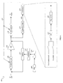
- a dynamically controlled integrated LNA system 400 may comprise a tunable input load 402 , an LNA 404 , a tunable output load 406 , a crystal oscillator (XTAL) 408 , a phase locked loop (PLL) 410 , a local oscillator (LO) generator 412 , switches 414 , a logarithmic amplifier 416 , and a control block 418 .
- XTAL crystal oscillator
- PLL phase locked loop
- LO local oscillator
- the LNA 404 may correspond to an integrated LNA such as the variable gain LNAs 150 a , 150 b , and 150 c described in FIGS. 1C-1D , for example.
- the logarithmic amplifier 416 may provide the same or substantially similar RSSI measuring operations as the logarithmic amplifier 172 described in FIGS. 1C-1D , for example.
- the XTAL 408 may be a reference crystal frequency such as the crystal 178 described in FIGS. 1C-1D , for example.
- the PLL 410 may comprise suitable logic, circuitry, and/or code that may enable generating a reference signal that may be utilized by the LO generator 412 .
- the operations provided by the PLL 410 may the same or substantially similar to those provided by the ⁇ - ⁇ fractional-N synthesizer 174 described in FIGS. 1C-1D , for example.
- a ⁇ - ⁇ fractional-N synthesizer by using a ⁇ - ⁇ fractional-N synthesizer, practically any frequency within the wanted range may be generated using a wide range of XTAL reference frequencies, which may allow optimization of the LNA tuning at arbitrary ranges within the wanted band of operation.
- the LO generator 412 may comprise suitable logic, circuitry, and/or code that may enable the generation of a single tone or single frequency signal that may be utilized to calibrate the gain provided by the tuning curve of the LNA 404 .
- the operations provided by the LO generator 412 may be the same or substantially similar to those provided by the VCO block 176 and/or the LO signal dividers 156 a and 156 b described in FIGS. 1C-1D , for example.
- the tunable input load 402 may comprise suitable logic, circuitry, and/or code that may enable dynamically controlling of a tuning curve associated with the LNA 404 .
- the tuning curve may be dynamically controlled by the digital control signal 420 generated by the control block 418 .
- the tunable input load 402 may be implemented using a capacitor bank, for example.
- the tunable output load 406 may comprise suitable logic, circuitry, and/or code that may enable dynamically controlling of the tuning curve associated with the LNA 404 .
- the tuning curve may be dynamically controlled by the digital control signal 420 generated by the control block 418 .
- the tunable output load 406 may be implemented using a capacitor bank, for example.
- the control block 418 may comprise suitable logic, circuitry, and/or code that may enable generation of the digital control signal 420 to adjust the tuning curve of the LNA 404 by adjusting the tunable input load 402 and/or the tunable output load 406 .
- the control block 418 may correspond to the gain control block 188 described in FIG. 1D .
- the signal AGC_RF 137 b may correspond to the digital control signal 420 , for example.
- control block 418 may comprise an ADC 422 and a digital control 424 .
- the ADC 422 may be the same or substantially similar to the ADC 134 described in FIG. 1B and the digital control 424 may be implemented within the digital baseband processor 132 also as described in FIG. 1B .
- the ADC 422 may comprise suitable logic, circuitry, and/or code that may enable analog-to-digital conversion of either an RSSI measurement from the logarithmic amplifier 416 or a processed I component, such as signal 135 a in FIGS. 1B-1D , for example.
- the ADC 422 may enable analog-to-digital conversion of either an RSSI measurement from the logarithmic amplifier 416 or a processed Q component, such as signal 135 c in FIGS. 1B-1D .
- the digital control 424 may comprise suitable logic, circuitry, and/or code that may enable generation of a digital control signal, such as the digital control signal 420 , to adjust the tunable input load 402 and/or the tunable output load 404 .
- the switches 414 may comprise suitable logic, circuitry, and/or code that may enable selecting whether to introduce the single tone or single frequency signal generated by the LO generator 412 to the input of the tunable input load 402 and/or to the output of the LNA 404 to generate an RSSI measurement.
- the single tone or single frequency signal may be introduced during a calibration mode. For example, for each new selected desired channel of operation, the RF receiver may perform a calibration or tuning curve adjustment of the LNA 404 before normal gain operations. At least one signal may be utilized to select whether the single tone or single frequency signal is to be introduced to the input of the tunable input load 402 , to the output of the LNA 404 , or to both.
- the dynamically controlled integrated LNA system 400 may be operated in a calibration mode to adjust the tuning curve of the LNA 404 for a currently selected desired channel of operation.
- the XTAL 408 may generate a reference signal that may be utilized by the PLL 410 to generate a signal that in turn may be utilized by the LO generator 412 to generate the single tone or single frequency signal that corresponds to the currently selected operating channel.
- the switches 414 may be utilized to introduce the single tone to the input of the tunable input load 402 and/or to the output of the LNA 404 .
- the output generated by the LNA 404 may be measured by the logarithmic amplifier 416 to generate an RSSI signal.
- the RSSI signal may be communicated to the control block 418 where the ADC 422 may digitize it.
- the digitized RSSI signal may be communicated to the digital control 424 where the digital control signal 420 may be generated to adjust the tunable input load 402 and/or the tunable output load 406 to achieve the appropriate tuning curve for the currently selected desired channel of operation. Once the tuning curve is properly adjusted, the dynamically controlled integrated LNA system 400 may operate in a normal mode of operation.
- FIG. 5 is a schematic diagram illustrating an exemplary integrated LNA with tunable input load and tunable output load, in accordance with an embodiment of the invention.
- an integrated LNA 500 with a tunable input capacitor bank (Cb 1 ) 508 and a tunable output capacitor bank (Cb 2 ) 518 .
- the integrated LNA 500 may comprise a first transistor (M 1 ) 512 , a second transistor (M 2 ) 514 , an inductor Ls 510 , and an inductor Ld 516 .
- the LNA 500 may also be implemented as a fully differential, that is, a balanced structure, and may communicate with PCB components, such as the balums 146 a , 146 b , and 146 c illustrated in FIGS. 1C-1D , via PCB traces that comprise series inductive components such as L PCB 506 , for example.
- PCB components such as the balums 146 a , 146 b , and 146 c illustrated in FIGS. 1C-1D , via PCB traces that comprise series inductive components such as L PCB 506 , for example.
- the tunable input capacitor bank (Cb 1 ) 508 may comprise a plurality of capacitors wherein the appropriate capacitance value for the Cb 1 508 may be selected by the digital control signal 420 described in FIG. 4 to adjust the tuning curve of the LNA 500 in accordance with a currently selected desired channel of operation.
- the Cb 1 508 may be implemented in parallel to the Ls 510 with one end of the capacitors connected to the gate of M 1 512 and the other end connected to GND 502 .
- the tunable output capacitor bank (Cb 2 ) 518 may comprise a plurality of capacitors wherein the appropriate capacitance value selected for the Cb 2 518 may be selected by the digital control signal 420 to adjust the tuning curve of the LNA 500 in accordance with a currently selected desired channel of operation.
- the Cb 2 518 may be implemented in parallel to the Ld 516 with one end of the capacitors connected to the drain of M 2 514 and the other end connected to Vdd 504 .
- the switches 414 may comprise a first RF switch 414 a and a second RF switch 414 b .
- the first RF switch 414 a and the second RF switch 414 b may comprise suitable logic, circuitry, and/or code that may enable selecting whether to introduce the single tone or single frequency for calibrating or adjusting the LNA 500 tuning curve at the gate of M 1 512 , at the drain of M 2 514 , or at both locations.
- the first RF switch 414 a enables introducing the single tone or single frequency signal at the drain of M 2 514
- the second RF switch 414 b enables introducing the single tone or single frequency signal at the gate of M 1 512 , for example.
- the output of the LNA 500 may be measured by the logarithmic amplifier 416 to generate an RSSI signal that may be utilized to adjust the Cb 1 508 and/or the Cb 2 518 to dynamically control the tuning curve of the LNA 500 to optimize the gain behavior of the LNA 500 for a currently selected desired operating channel.
- FIGS. 6A and 6B are flow diagrams illustrating exemplary steps in the calibration of a dynamically controlled variable gain LNA for a selected desired channel, in accordance with an embodiment of the invention.
- a flow chart 600 there is shown a flow chart 600 .
- a desired channel of operation is selected.
- a single tone or single frequency signal that corresponds to the selected desired channel may be generated by the LO generator 412 to generate an output from the dynamically controlled variable gain LNA.
- the single tone or single frequency signal may be applied to the input of the tunable input load 402 or to the output of the dynamically controlled variable gain LNA.
- the input of the tunable input load 402 corresponds to one end of the Cb 1 508 while the output of the dynamically controlled variable gain LNA corresponds to one end of the Cb 2 518 .
- At least one signal may be generated to determine where to introduce the single tone or single frequency signal.
- the switches 414 may be configured based on the signals generated.
- the output of the dynamically controlled variable gain LNA may be measured by the logarithmic amplifier 416 to determine an RSSI value.
- the control block 418 may generate the digital control signal 420 to adjust the tunable input load 402 or the tunable output load 406 .
- the calibration operation may be completed and the single-chip multi-band RF receiver 140 a may enable a general or normal gain mode of operation for the dynamically controlled variable gain LNA.
- the single-chip multi-band RF receiver 140 a may determine whether to select a new desired operating channel. When the new desired channel is selected, the process may proceed to step 604 . In instances where the new desired channel is not selected, the process may proceed to end step 618 .
- the calibration operation may require a new reading of the dynamically controlled variable gain LNA output to generate an updated RSSI value for each adjustment made to the tunable input load 402 and/or the tunable output load 406 .
- the steps 610 and 612 may be repeated iteratively multiple times until the tuning curve of the dynamically controlled variable gain LNA achieves a determined performance for the selected desired channel of operation. This may be achieved when the RSSI reading indicates that the gain is maximized for the available tuning range for the specific LO input injected at the input or output load.
- the process may again proceed to step 614 where the single-chip multi-band RF receiver 140 a may terminate the calibration operation and may proceed to enable a general or normal gain mode of operation.
- the single tone or single frequency signal generated by the LO generator 412 that corresponds to the selected desired channel may be applied to a first tunable load communicatively coupled to the dynamically controlled variable gain LNA.
- the first tunable load may be the input or the output load.
- the output of the dynamically controlled variable gain LNA may be measured by the logarithmic amplifier 416 to determine an RSSI value.
- the control block 418 may determine whether the RSSI measurement indicates that a maximum gain is achieved by the dynamically controlled variable gain LNA. When a maximum gain is not achieved, the process may proceed to step 630 .
- the control block 418 may generate a digital control signal to adjust the first tunable load.
- step 632 when the RSSI measurement indicates that a maximum gain is achieved, the process may proceed to step 632 .
- the calibration process may require that a second tunable load communicatively coupled to the dynamically controlled variable gain LNA also be calibrated.
- the second tunable load may be the input or output load not yet calibrated.
- the process may proceed to step 634 .
- step 634 the single tone or single frequency signal generated by the LO generator 412 that corresponds to the selected desired channel may be applied to the second tunable load of the dynamically controlled variable gain LNA.
- steps 626 and 628 When a maximum gain is not achieved in step 628 , the process may proceed to step 630 where the control block 418 may generate a digital control signal to adjust the second tunable load.
- step 632 when the calibration process does not require that a second tunable load communicatively coupled to the dynamically controlled variable gain LNA be calibrated or when calibration of the second tunable load has been completed, the process may proceed to step 636 .
- step 636 the single-chip multi-band RF receiver 140 a may terminate the calibration operation and may proceed to enable a general or normal gain mode of operation.
- the present invention may be realized in hardware, software, or a combination of hardware and software.
- the present invention may be realized in a centralized fashion in at least one computer system, or in a distributed fashion where different elements are spread across several interconnected computer systems. Any kind of computer system or other apparatus adapted for carrying out the methods described herein is suited.
- a typical combination of hardware and software may be a general-purpose computer system with a computer program that, when being loaded and executed, controls the computer system such that it carries out the methods described herein.
- the present invention may also be embedded in a computer program product, which comprises all the features enabling the implementation of the methods described herein, and which when loaded in a computer system is able to carry out these methods.
- Computer program in the present context means any expression, in any language, code or notation, of a set of instructions intended to cause a system having an information processing capability to perform a particular function either directly or after either or both of the following: a) conversion to another language, code or notation; b) reproduction in a different material form.
Landscapes
- Physics & Mathematics (AREA)
- Electromagnetism (AREA)
- Engineering & Computer Science (AREA)
- Computer Networks & Wireless Communication (AREA)
- Signal Processing (AREA)
- Circuits Of Receivers In General (AREA)
- Superheterodyne Receivers (AREA)
Abstract
Description
Claims (22)
Priority Applications (1)
| Application Number | Priority Date | Filing Date | Title |
|---|---|---|---|
| US12/709,974 US8081941B2 (en) | 2006-03-02 | 2010-02-22 | Method and system for RF front-end calibration scheme using fractional-N frequency synthesized signals and RSSI |
Applications Claiming Priority (3)
| Application Number | Priority Date | Filing Date | Title |
|---|---|---|---|
| US77823206P | 2006-03-02 | 2006-03-02 | |
| US11/432,450 US7668521B2 (en) | 2006-03-02 | 2006-05-11 | Method and system for RF front-end calibration scheme using fractional-N frequency synthesized signals and RSSI |
| US12/709,974 US8081941B2 (en) | 2006-03-02 | 2010-02-22 | Method and system for RF front-end calibration scheme using fractional-N frequency synthesized signals and RSSI |
Related Parent Applications (1)
| Application Number | Title | Priority Date | Filing Date |
|---|---|---|---|
| US11/432,450 Continuation US7668521B2 (en) | 2006-03-02 | 2006-05-11 | Method and system for RF front-end calibration scheme using fractional-N frequency synthesized signals and RSSI |
Publications (2)
| Publication Number | Publication Date |
|---|---|
| US20100167673A1 US20100167673A1 (en) | 2010-07-01 |
| US8081941B2 true US8081941B2 (en) | 2011-12-20 |
Family
ID=38472041
Family Applications (2)
| Application Number | Title | Priority Date | Filing Date |
|---|---|---|---|
| US11/432,450 Active 2028-07-24 US7668521B2 (en) | 2006-03-02 | 2006-05-11 | Method and system for RF front-end calibration scheme using fractional-N frequency synthesized signals and RSSI |
| US12/709,974 Expired - Fee Related US8081941B2 (en) | 2006-03-02 | 2010-02-22 | Method and system for RF front-end calibration scheme using fractional-N frequency synthesized signals and RSSI |
Family Applications Before (1)
| Application Number | Title | Priority Date | Filing Date |
|---|---|---|---|
| US11/432,450 Active 2028-07-24 US7668521B2 (en) | 2006-03-02 | 2006-05-11 | Method and system for RF front-end calibration scheme using fractional-N frequency synthesized signals and RSSI |
Country Status (1)
| Country | Link |
|---|---|
| US (2) | US7668521B2 (en) |
Families Citing this family (16)
| Publication number | Priority date | Publication date | Assignee | Title |
|---|---|---|---|---|
| US7877070B2 (en) * | 2006-09-29 | 2011-01-25 | Broadcom Corp. | Method and system for tuning an antenna using injection |
| US8284822B2 (en) * | 2007-02-27 | 2012-10-09 | Broadcom Corporation | Method and system for utilizing direct digital frequency synthesis to process signals in multi-band applications |
| US7586458B2 (en) * | 2007-03-19 | 2009-09-08 | Ahmadreza Rofougaran | Method and system for using a transformer for FM transmit and FM receive functionality |
| US7929932B2 (en) * | 2007-09-26 | 2011-04-19 | Intel Corporation | Removing harmonic and co-existence interference in radio receivers |
| US7890069B2 (en) * | 2007-11-09 | 2011-02-15 | Broadcom Corporation | Selectable low noise amplifier for wireless communication |
| US8976302B2 (en) * | 2009-09-30 | 2015-03-10 | Wi-Lan, Inc. | Radio frequency front end for television band receiver and spectrum sensor |
| US9544004B2 (en) | 2010-03-12 | 2017-01-10 | Sunrise Micro Devices, Inc. | Power efficient communications |
| CN102749511B (en) | 2012-06-12 | 2015-08-12 | 大唐移动通信设备有限公司 | Distributed frequency spectrum analyser and apply the method that it carries out spectrum analysis |
| US8954019B2 (en) * | 2012-08-03 | 2015-02-10 | Blackberry Limited | Mobile wireless communications device with LNA front end circuit and related methods |
| WO2014117341A1 (en) * | 2013-01-30 | 2014-08-07 | Telefonaktiebolaget L M Ericsson (Publ) | Method and apparatus for calibrating multiple antennas |
| WO2015045709A1 (en) * | 2013-09-26 | 2015-04-02 | 日本電気株式会社 | Signal transmission apparatus, distortion compensation apparatus, and signal transmission method |
| US9577688B2 (en) * | 2015-02-24 | 2017-02-21 | Qualcomm Technologies International, Ltd. | Frequency tuning of narrowband low noise amplifiers |
| WO2017068852A1 (en) * | 2015-10-19 | 2017-04-27 | 株式会社村田製作所 | High-frequency front-end circuit, and method for suppressing unwanted wave |
| RU180109U9 (en) * | 2017-12-14 | 2018-08-06 | Российская Федерация, от имени которой выступает Государственная корпорация по космической деятельности "РОСКОСМОС" | Transceiver module of the C-band digital active phased array antenna |
| CN109039294B (en) * | 2018-08-08 | 2022-02-18 | 义乌工商职业技术学院 | Automatic correcting circuit for computer signal |
| FR3120279B1 (en) | 2021-02-26 | 2024-01-05 | St Microelectronics Grenoble 2 | Calibration of an RF attenuator |
Citations (3)
| Publication number | Priority date | Publication date | Assignee | Title |
|---|---|---|---|---|
| US5907798A (en) | 1996-06-21 | 1999-05-25 | Lucent Technologies Inc. | Wireless telephone intermodulation performance enhancement techniques |
| US6978125B2 (en) | 2001-07-05 | 2005-12-20 | Telefonaktiebolaget Lm Ericsson (Publ) | Methods and apparatus for tuning pre-selection filters in radio receivers |
| US20060068740A1 (en) | 2004-09-24 | 2006-03-30 | Matsushita Electric Industrial Co., Ltd. | Receiver if circuit including image rejection mixer and active bandpass filter |
-
2006
- 2006-05-11 US US11/432,450 patent/US7668521B2/en active Active
-
2010
- 2010-02-22 US US12/709,974 patent/US8081941B2/en not_active Expired - Fee Related
Patent Citations (3)
| Publication number | Priority date | Publication date | Assignee | Title |
|---|---|---|---|---|
| US5907798A (en) | 1996-06-21 | 1999-05-25 | Lucent Technologies Inc. | Wireless telephone intermodulation performance enhancement techniques |
| US6978125B2 (en) | 2001-07-05 | 2005-12-20 | Telefonaktiebolaget Lm Ericsson (Publ) | Methods and apparatus for tuning pre-selection filters in radio receivers |
| US20060068740A1 (en) | 2004-09-24 | 2006-03-30 | Matsushita Electric Industrial Co., Ltd. | Receiver if circuit including image rejection mixer and active bandpass filter |
Non-Patent Citations (4)
| Title |
|---|
| EICTA-European Industry Association, Information Systems Communication Technologies Consumer Electronics, EICTA/TAC/MBRAI-0216, "Mobile and Portable DVB-T Radio Access Interface Specification", Version 1.0, Jan. 1, 2004, pp. 1-46. |
| Mark Dawkins, Alison Payne Burnett, Nick Cowley, "A Single-Chip Tuner for DVB-T", IEEE Journal of Solid-State Circuits, vol. 38, No. 8, Aug. 2003, pp. 1307-1317. |
| Patrick Antonine, et al., "A Direct-Conversion Receiver for DVB-H", IEEE Journal of Solid-State Circuits, vol. 40, No. 12, Dec. 2005, pp. 2536-2546. |
| Takeuchi et al. "asingle chip RF front end for the digital sound broadcasting" by SONY Corporation. Jun. 25, 2001. |
Also Published As
| Publication number | Publication date |
|---|---|
| US20100167673A1 (en) | 2010-07-01 |
| US7668521B2 (en) | 2010-02-23 |
| US20070207759A1 (en) | 2007-09-06 |
Similar Documents
| Publication | Publication Date | Title |
|---|---|---|
| US8081941B2 (en) | Method and system for RF front-end calibration scheme using fractional-N frequency synthesized signals and RSSI | |
| US7706766B2 (en) | Method and system for a programmable biasing mechanism for a mobile digital television environment | |
| US7924944B2 (en) | Method and system for multi-band direct conversion complimentary metal-oxide-semiconductor (CMOS) mobile television tuner | |
| US7680227B2 (en) | Method and system for filter calibration using fractional-N frequency synthesized signals | |
| US7969222B2 (en) | Method and system for DC offset correction loop for a mobile digital cellular television environment | |
| US8463219B2 (en) | Programmable baseband filters supporting auto-calibration for a mobile digital cellular television environment | |
| US7127217B2 (en) | On-chip calibration signal generation for tunable filters for RF communications and associated methods | |
| US8284822B2 (en) | Method and system for utilizing direct digital frequency synthesis to process signals in multi-band applications | |
| US7890069B2 (en) | Selectable low noise amplifier for wireless communication | |
| US7471940B2 (en) | Ratiometric clock systems for integrated receivers and associated methods | |
| US7634237B2 (en) | Method and system for a fractional-N synthesizer for a mobile digital cellular television environment | |
| US8145172B2 (en) | Low-cost receiver using tracking filter | |
| US20070042734A1 (en) | Tuner and broadcasting signal receiver including the same | |
| US20080261548A1 (en) | System and method for selecting an intermediate frequency | |
| US20070064843A1 (en) | Method and system for mobile cellular television tuner utilizing current-steering variable gain at RF | |
| US20100130155A1 (en) | Low-Cost Receiver Using Tracking Bandpass Filter and Lowpass Filter | |
| WO2006109296A2 (en) | A method for tuning an rf base-band circuit of a receiver | |
| Kang et al. | A triband 65nm CMOS tuner for ATSC mobile DTV SoC | |
| US20070178863A1 (en) | AM/FM tuner saw filter-less architecture using AM frequency band up-conversion | |
| Vassiliou et al. | CMOS tuners for mobile TV | |
| KR20110040407A (en) | Tuner circuit | |
| Iason et al. | Overview of Mobile TV Standards and their CMOS Tuners | |
| Vassiliou et al. | Overview of Mobile TV Standards and their CMOS Tuners | |
| Albasha | System challenges in the design of a broadband RFIC receiver for DVB-H mobile systems |
Legal Events
| Date | Code | Title | Description |
|---|---|---|---|
| ZAAA | Notice of allowance and fees due |
Free format text: ORIGINAL CODE: NOA |
|
| ZAAB | Notice of allowance mailed |
Free format text: ORIGINAL CODE: MN/=. |
|
| STCF | Information on status: patent grant |
Free format text: PATENTED CASE |
|
| FPAY | Fee payment |
Year of fee payment: 4 |
|
| AS | Assignment |
Owner name: BANK OF AMERICA, N.A., AS COLLATERAL AGENT, NORTH CAROLINA Free format text: PATENT SECURITY AGREEMENT;ASSIGNOR:BROADCOM CORPORATION;REEL/FRAME:037806/0001 Effective date: 20160201 Owner name: BANK OF AMERICA, N.A., AS COLLATERAL AGENT, NORTH Free format text: PATENT SECURITY AGREEMENT;ASSIGNOR:BROADCOM CORPORATION;REEL/FRAME:037806/0001 Effective date: 20160201 |
|
| AS | Assignment |
Owner name: AVAGO TECHNOLOGIES GENERAL IP (SINGAPORE) PTE. LTD., SINGAPORE Free format text: ASSIGNMENT OF ASSIGNORS INTEREST;ASSIGNOR:BROADCOM CORPORATION;REEL/FRAME:041706/0001 Effective date: 20170120 Owner name: AVAGO TECHNOLOGIES GENERAL IP (SINGAPORE) PTE. LTD Free format text: ASSIGNMENT OF ASSIGNORS INTEREST;ASSIGNOR:BROADCOM CORPORATION;REEL/FRAME:041706/0001 Effective date: 20170120 |
|
| AS | Assignment |
Owner name: BROADCOM CORPORATION, CALIFORNIA Free format text: TERMINATION AND RELEASE OF SECURITY INTEREST IN PATENTS;ASSIGNOR:BANK OF AMERICA, N.A., AS COLLATERAL AGENT;REEL/FRAME:041712/0001 Effective date: 20170119 |
|
| AS | Assignment |
Owner name: AVAGO TECHNOLOGIES INTERNATIONAL SALES PTE. LIMITE Free format text: MERGER;ASSIGNOR:AVAGO TECHNOLOGIES GENERAL IP (SINGAPORE) PTE. LTD.;REEL/FRAME:047196/0687 Effective date: 20180509 |
|
| AS | Assignment |
Owner name: AVAGO TECHNOLOGIES INTERNATIONAL SALES PTE. LIMITE Free format text: CORRECTIVE ASSIGNMENT TO CORRECT THE EFFECTIVE DATE OF MERGER TO 9/5/2018 PREVIOUSLY RECORDED AT REEL: 047196 FRAME: 0687. ASSIGNOR(S) HEREBY CONFIRMS THE MERGER;ASSIGNOR:AVAGO TECHNOLOGIES GENERAL IP (SINGAPORE) PTE. LTD.;REEL/FRAME:047630/0344 Effective date: 20180905 |
|
| AS | Assignment |
Owner name: AVAGO TECHNOLOGIES INTERNATIONAL SALES PTE. LIMITE Free format text: CORRECTIVE ASSIGNMENT TO CORRECT THE PROPERTY NUMBERS PREVIOUSLY RECORDED AT REEL: 47630 FRAME: 344. ASSIGNOR(S) HEREBY CONFIRMS THE ASSIGNMENT;ASSIGNOR:AVAGO TECHNOLOGIES GENERAL IP (SINGAPORE) PTE. LTD.;REEL/FRAME:048883/0267 Effective date: 20180905 |
|
| MAFP | Maintenance fee payment |
Free format text: PAYMENT OF MAINTENANCE FEE, 8TH YEAR, LARGE ENTITY (ORIGINAL EVENT CODE: M1552); ENTITY STATUS OF PATENT OWNER: LARGE ENTITY Year of fee payment: 8 |
|
| FEPP | Fee payment procedure |
Free format text: MAINTENANCE FEE REMINDER MAILED (ORIGINAL EVENT CODE: REM.); ENTITY STATUS OF PATENT OWNER: LARGE ENTITY |
|
| LAPS | Lapse for failure to pay maintenance fees |
Free format text: PATENT EXPIRED FOR FAILURE TO PAY MAINTENANCE FEES (ORIGINAL EVENT CODE: EXP.); ENTITY STATUS OF PATENT OWNER: LARGE ENTITY |
|
| STCH | Information on status: patent discontinuation |
Free format text: PATENT EXPIRED DUE TO NONPAYMENT OF MAINTENANCE FEES UNDER 37 CFR 1.362 |
|
| FP | Lapsed due to failure to pay maintenance fee |
Effective date: 20231220 |