US8080472B2 - Metal line having a MoxSiy/Mo diffusion barrier of semiconductor device and method for forming the same - Google Patents
Metal line having a MoxSiy/Mo diffusion barrier of semiconductor device and method for forming the same Download PDFInfo
- Publication number
- US8080472B2 US8080472B2 US12/472,721 US47272109A US8080472B2 US 8080472 B2 US8080472 B2 US 8080472B2 US 47272109 A US47272109 A US 47272109A US 8080472 B2 US8080472 B2 US 8080472B2
- Authority
- US
- United States
- Prior art keywords
- layer
- metal line
- forming region
- diffusion barrier
- metal
- Prior art date
- Legal status (The legal status is an assumption and is not a legal conclusion. Google has not performed a legal analysis and makes no representation as to the accuracy of the status listed.)
- Expired - Fee Related, expires
Links
Images


Classifications
-
- H—ELECTRICITY
- H10—SEMICONDUCTOR DEVICES; ELECTRIC SOLID-STATE DEVICES NOT OTHERWISE PROVIDED FOR
- H10D—INORGANIC ELECTRIC SEMICONDUCTOR DEVICES
- H10D64/00—Electrodes of devices having potential barriers
- H10D64/01—Manufacture or treatment
- H10D64/011—Manufacture or treatment of electrodes ohmically coupled to a semiconductor
-
- H—ELECTRICITY
- H10—SEMICONDUCTOR DEVICES; ELECTRIC SOLID-STATE DEVICES NOT OTHERWISE PROVIDED FOR
- H10W—GENERIC PACKAGES, INTERCONNECTIONS, CONNECTORS OR OTHER CONSTRUCTIONAL DETAILS OF DEVICES COVERED BY CLASS H10
- H10W20/00—Interconnections in chips, wafers or substrates
- H10W20/01—Manufacture or treatment
- H10W20/031—Manufacture or treatment of conductive parts of the interconnections
- H10W20/032—Manufacture or treatment of conductive parts of the interconnections of conductive barrier, adhesion or liner layers
- H10W20/033—Manufacture or treatment of conductive parts of the interconnections of conductive barrier, adhesion or liner layers in openings in dielectrics
- H10W20/035—Manufacture or treatment of conductive parts of the interconnections of conductive barrier, adhesion or liner layers in openings in dielectrics combinations of barrier, adhesion or liner layers, e.g. multi-layered barrier layers
-
- H—ELECTRICITY
- H10—SEMICONDUCTOR DEVICES; ELECTRIC SOLID-STATE DEVICES NOT OTHERWISE PROVIDED FOR
- H10W—GENERIC PACKAGES, INTERCONNECTIONS, CONNECTORS OR OTHER CONSTRUCTIONAL DETAILS OF DEVICES COVERED BY CLASS H10
- H10W20/00—Interconnections in chips, wafers or substrates
- H10W20/01—Manufacture or treatment
- H10W20/031—Manufacture or treatment of conductive parts of the interconnections
- H10W20/032—Manufacture or treatment of conductive parts of the interconnections of conductive barrier, adhesion or liner layers
- H10W20/042—Manufacture or treatment of conductive parts of the interconnections of conductive barrier, adhesion or liner layers the barrier, adhesion or liner layers being seed or nucleation layers
- H10W20/043—Manufacture or treatment of conductive parts of the interconnections of conductive barrier, adhesion or liner layers the barrier, adhesion or liner layers being seed or nucleation layers for electroplating
-
- H—ELECTRICITY
- H10—SEMICONDUCTOR DEVICES; ELECTRIC SOLID-STATE DEVICES NOT OTHERWISE PROVIDED FOR
- H10W—GENERIC PACKAGES, INTERCONNECTIONS, CONNECTORS OR OTHER CONSTRUCTIONAL DETAILS OF DEVICES COVERED BY CLASS H10
- H10W20/00—Interconnections in chips, wafers or substrates
- H10W20/01—Manufacture or treatment
- H10W20/031—Manufacture or treatment of conductive parts of the interconnections
- H10W20/032—Manufacture or treatment of conductive parts of the interconnections of conductive barrier, adhesion or liner layers
- H10W20/047—Manufacture or treatment of conductive parts of the interconnections of conductive barrier, adhesion or liner layers by introducing additional elements therein
- H10W20/048—Manufacture or treatment of conductive parts of the interconnections of conductive barrier, adhesion or liner layers by introducing additional elements therein by using plasmas or gaseous environments, e.g. by nitriding
-
- H—ELECTRICITY
- H10—SEMICONDUCTOR DEVICES; ELECTRIC SOLID-STATE DEVICES NOT OTHERWISE PROVIDED FOR
- H10W—GENERIC PACKAGES, INTERCONNECTIONS, CONNECTORS OR OTHER CONSTRUCTIONAL DETAILS OF DEVICES COVERED BY CLASS H10
- H10W20/00—Interconnections in chips, wafers or substrates
- H10W20/40—Interconnections external to wafers or substrates, e.g. back-end-of-line [BEOL] metallisations or vias connecting to gate electrodes
- H10W20/41—Interconnections external to wafers or substrates, e.g. back-end-of-line [BEOL] metallisations or vias connecting to gate electrodes characterised by their conductive parts
- H10W20/425—Barrier, adhesion or liner layers
-
- Y—GENERAL TAGGING OF NEW TECHNOLOGICAL DEVELOPMENTS; GENERAL TAGGING OF CROSS-SECTIONAL TECHNOLOGIES SPANNING OVER SEVERAL SECTIONS OF THE IPC; TECHNICAL SUBJECTS COVERED BY FORMER USPC CROSS-REFERENCE ART COLLECTIONS [XRACs] AND DIGESTS
- Y10—TECHNICAL SUBJECTS COVERED BY FORMER USPC
- Y10T—TECHNICAL SUBJECTS COVERED BY FORMER US CLASSIFICATION
- Y10T428/00—Stock material or miscellaneous articles
- Y10T428/24—Structurally defined web or sheet [e.g., overall dimension, etc.]
- Y10T428/24479—Structurally defined web or sheet [e.g., overall dimension, etc.] including variation in thickness
- Y10T428/24612—Composite web or sheet
Definitions
- the present invention relates to metal lines semiconductor devices and to methods for forming the same, and more particularly, to a metal line having of a Mo x Si y /Mo stacked diffusion barrier that inhibits copper diffusion.
- metal lines are in a semiconductor device to electrically connect together various elements or lines with each other.
- Contact plugs are formed to electrically connect together lower metal lines and upper metal lines to each other.
- the aspect ratios of contact holes in which contact plugs are formed also gradually increases.
- the process for forming metal lines and contact plugs become more difficult because these diminutive metal lines and contact plugs must also maintain their physical and performance characteristics such as assuring that unwanted impurities do not diffuse past their respective corresponding diffusion barriers.
- Copper and tungsten have been mainly used as suitable conductive materials in the metal lines of a semiconductor devices because they exhibit relatively good electrical conductivity properties and because they do not tend towards adversely affecting the performance of the resultant semiconductor device due to unwanted diffusion away from these metal lines. Recently, research has been made in the hopes of using copper as a next-generation material for a metal line because copper exhibits a superior electrical conductivity and a corresponding low resistance as compared to aluminum and tungsten. Copper (Cu) can therefore solve or at least aid in minimizing the problems associated with RC (resistance-capacitance) signal delay in the semiconductor device having a high level of integration and high operating speed.
- RC resistance-capacitance
- a metal line forming region is defined by etching the insulation layer. Then, a diffusion barrier is formed on the insulation layer and on the surface of the metal line forming region, and a copper seed layer is subsequently formed on the diffusion barrier. Next, after forming a copper layer on the copper seed layer, a metal line comprising the copper layer is formed by CMPing (chemically and mechanically polishing) the copper layer.
- the thickness of the diffusion barrier should also decrease. Therefore, it is becoming more difficult to properly prevent the diffusion of a copper constituent by means of the diffusion barrier formed in accordance to the conventional art techniques. Furthermore, in the conventional art described above, it is becoming more and more difficult to increase the thickness of the diffusion barrier so as to improve the characteristics of the diffusion barrier and thereby as a result the characteristics of the subsequent diffusion barrier deteriorate. In addition, in the conventional art described above, an unwanted overhang phenomenon can occur due to the conglomeration of the copper seed layer formed on the diffusion barrier. Because of this conglomeration of copper, the entrance to the metal line forming region is prone to being clogged, and as a consequence unwanted voids can be created in the metal line and thus the characteristics of the metal line can deteriorate.
- Embodiments of the present invention are directed to a metal line of a semiconductor device that can result in improving the characteristics of a diffusion barrier and a method for forming the same.
- embodiments of the present invention are directed to a metal line of a semiconductor device that can exhibit improved characteristics and enhanced reliability of a resultant semiconductor device and a method for forming the same.
- a metal line of a semiconductor device comprises an insulation layer formed on a semiconductor substrate and having a metal line forming region; a diffusion barrier formed on a surface of the metal line forming region of the insulation layer and having a stack structure of an Mo x Si y layer and an Mo layer; and a metal layer formed on the diffusion barrier to fill the metal line forming region of the insulation layer.
- the x subscript is a real number that has a preferable range of about 1 ⁇ 10
- the y subscript is a real number that has a preferable range of about 1 ⁇ 10.
- the Mo x Si y layer has a preferable thickness of about 5 ⁇ 100 ⁇ .
- the Mo layer has a preferable thickness of about 5 ⁇ 400 ⁇ .
- the metal layer may be any conductive material such as polysilicon, aluminum, tungsten in which it is preferable that the metal layer comprises a copper.
- a method for forming a metal line of a semiconductor device comprises the steps of forming an insulation layer on a semiconductor substrate to have a metal line forming region; forming a diffusion barrier on the insulation layer including a surface of the metal line forming region to have a stack structure of an Mo x Si y layer and an Mo layer; and forming a metal layer on the diffusion barrier to substantially fill in the metal line forming region.
- the step of forming the diffusion barrier comprises the steps of forming a first Mo layer on the insulation layer including a surface of the metal line forming region; silicidating the first Mo layer and thereby converting the first Mo layer into an Mo x Si y layer; and forming a second Mo layer on the Mo x Si y layer.
- Silicidation of the first Mo layer is implemented for about 1 ⁇ 30 minutes.
- the silicidation of the first Mo layer is implemented under a pressure of about 1 ⁇ 760 mtorr.
- the silicidation of the first Mo layer is implemented at a temperature of about 25 ⁇ 400° C.
- the step of silicidating the first Mo layer comprises the steps of plasma-processing the first Mo layer; and soaking the plasma-processed first Mo layer in an SiH 4 atmosphere.
- the step of forming the first Mo layer and the step of silicidating the first Mo layer and thereby converting the first Mo layer into the Mo x Si y layer can be repeatedly implemented about 1 ⁇ 50 times.
- the step of forming the second Mo layer can be implemented at a temperature of about ⁇ 25 ⁇ 100° C.
- x is a real number that has a range of about 1 ⁇ 10
- y is a real number that has a range of about 1 ⁇ 10.
- the Mo x Si y layer is formed to have a thickness of about 5 ⁇ 100 ⁇ .
- the Mo layer is formed to have a thickness of about 5 ⁇ 400 ⁇ .
- the metal layer preferable comprises a copper layer.
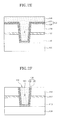
- FIG. 1 is a sectional view illustrating a metal line of a semiconductor device in accordance with an embodiment of the present invention.
- FIGS. 2A through 2F are sectional views illustrating the processes of a method for forming a metal line of a semiconductor device in accordance with another embodiment of the present invention.
- a diffusion barrier having the stack structure composed of a Mo x Si y layer and a Mo layer formed between an insulation layer and a copper layer By doing this, since the Mo constituent exhibits little or no solid-solved copper, the characteristics of the diffusion barrier having the stack structure of the Mo x Si y layer and the Mo layer are substantially improved. Also, since the Mo constituent exhibits excellent electrical conductivity due its very low resistance of 2.4 ⁇ /cm, then the diffusion barrier not only prevents the diffusion of the copper constituent but it also can serve as a seed layer for the copper layer.
- the present invention because it is not necessary to form a separate seed layer onto the diffusion barrier, then the unwanted overhang phenomenon of the copper layer can be reduced or avoided, and thus the creation of unwanted voids in the copper layer can be minimized.
- the characteristics of the metal line can be improved in comparison with the conventional art, whereby the characteristics and the reliability of a semiconductor device can be improved.
- FIG. 1 is a sectional view illustrating a metal line of a semiconductor device in accordance with an embodiment of the present invention.
- a first insulation layer 110 , an etch stop layer 112 and a second insulation layer 114 are formed on a semiconductor substrate 100 which is formed with a predetermined understructure (not shown), in such a way as to have a metal line forming region D.
- the metal line forming region D can be defined by using any known now methodology such as using a single damascene process or a dual damascene process.
- the metal forming region D may have any shape or structure such as having a trench structure or a trench and via-hole structure which has a trench and at least one via-hole communicating with the trench.
- the first and second insulation layers 110 and 114 may comprise any known type of insulation layers, such as, silicon oxide layers.
- the etch stop layer 112 may comprise any known etch stop layers, for example, a silicon nitride layer.
- a diffusion barrier 130 having the stack structure of an Mo x Si y layer 120 and an Mo layer 122 is formed on the surface of the metal line forming region D.
- the stoichiometry of the Mo x Si y layer 120 may be any known stochiometric ratio.
- the x subscript of the Mo x Si y layer 120 is a real number that has a range of about 1 ⁇ 10, and the y subscript is a real number that has a range of about 1 ⁇ 10.
- the Mo x Si y layer 120 may have any thickness in which it is preferred that Mo x Si y layer 120 has a thickness of about 5 ⁇ 100 ⁇ .
- the Mo layer 122 may be any thickness in which it is preferred that the Mo layer 122 has a thickness of about 5 ⁇ 400 ⁇ .
- a metal line 150 is then formed on the diffusion barrier 130 to substantially fill in the metal line forming region D.
- the metal line 150 may be composed of any electrically conductive material in which it is preferred that the metal line 150 comprises a copper layer.
- the diffusion barrier 130 has the stack structure of the Mo x Si y layer 120 and the Mo layer 122 , each layer has a Mo constituent which exhibits little or no solid-solved properties for copper. As a result, the characteristics of the resulting diffusion barrier 130 are substantially improved as compared to the conventional art. Accordingly, since the diffusion barrier 130 of the present application can prevent or at least significantly inhibit the diffusion of a copper constituent then a relatively thinner thickness of the diffusion barrier 130 is needed in the present invention. As a result, the characteristics of the diffusion barrier 130 can be effectively improved even without increasing the thickness thereof. Thereby the characteristics and the reliability of a semiconductor device can be improved.
- the molybdenum constituent of the diffusion barrier 130 in the present invention also exhibits excellent electrical conductivity, then the copper layer can be easily deposited even without the need for forming an additional seed layer on the diffusion barrier 130 .
- the overhang phenomenon brought about by the unwanted conglomeration of the seed layer can be reduced or avoided.
- creation of unwanted voids in the copper layer can be at least minimized and possibly avoided which in turn result in enhancing the performance characteristics of the resultant metal line of the present invention.
- FIGS. 2A through 2F are sectional views that illustrate some of the more important processes of a method for forming a metal line of a semiconductor device in accordance with another embodiment of the present invention.
- a first insulation layer 110 , an etch stop layer 112 and a second insulation layer 114 are sequentially formed on a semiconductor substrate 100 which is formed with a predetermined understructure (not shown), such that the understructure is covered.
- the first and second insulation layers 110 and 114 may comprise silicon oxide layers
- the etch stop layer 112 may comprise a silicon nitride layer.
- a metal line forming region D is defined.
- the metal line forming region D may be defined for a single damascene process or a dual damascene process to fill in the metal line forming region D.
- the metal line forming region D may have a trench structure or a trench and via-hole structure which has a trench and at least one via-hole communicating with the trench.
- a first Mo layer 120 a is formed on the second insulation layer 114 and on the surface of the metal line forming region D.
- the first Mo layer 120 a may be formed by any known methodology of depositing a molybdenum layer, such as using chemical vapor deposition (CVD), metal-organic CVD (MOCVD), plasma enhanced CVD (PECVD), evaporation, or physical vapor deposition (PVD) techniques.
- CVD chemical vapor deposition
- MOCVD metal-organic CVD
- PECVD plasma enhanced CVD
- PVD physical vapor deposition
- the first Mo layer 120 a is then silicidating which converts the first Mo layer 120 a into an Mo x Si y layer 120 .
- the silicidation of the first Mo layer 120 a is implemented preferable at a temperature below about 400° C., for example, about 25 ⁇ 400° C. under a pressure of about 1 ⁇ 760 mTorr within 30 minutes, preferably, for about 1 ⁇ 30 minutes.
- the silicidation of the first Mo layer 120 a is performed in a manner such that the first Mo layer 120 a is first plasma-processed to elevate the reactivity of the surface thereof and then, chemical soaking is executed.
- the chemical soaking is executed, for example, by preferably exposing the plasma-processed first Mo layer 120 a to a SiH 4 atmosphere.
- the process for forming the first Mo layer 120 a and the process for silicidating the first Mo layer 120 a can be repeatedly conducted about 1 ⁇ 50 times until the resultant Mo x Si y layer 120 has a desired thickness, preferably, about 5 ⁇ 100 ⁇ .
- a second Mo layer 122 is then subsequently formed on the Mo x Si y layer 120 .
- the second Mo layer 122 is also formed by any known deposition technique such as using CVD, MOCVD, PECVD, evaporation or PVD, preferably, at a temperature of about ⁇ 25 ⁇ 100° C.
- the second Mo layer 122 can be formed at any thickness, however it is preferred that the second Mo layer 122 is also formed at a thickness of about 5 ⁇ 400 ⁇ .
- a diffusion barrier 130 having the stack-like structure of the second Mo layer 122 stacked on top of the Mo x Si y layer 120 .
- a diffusion barrier 130 is formed on the second insulation layer 114 and on the surface of the metal line forming region D.
- a metal layer 140 is formed on the diffusion barrier 130 to fill the metal line forming region D.
- the metal layer 140 may comprise any conductive metal in which it is preferred that the metal layer 140 comprises a copper layer.
- the copper layer is preferably formed using electroplating. Since the diffusion barrier 130 has a molybdenum constituent that has an excellent electrical conductivity property, then the metal layer 140 can be formed without the need for additionally forming a seed layer on the diffusion barrier 130 .
- a stacked diffusion barrier having a Mo x Si y layer stacked underneath a Mo layer is formed. Since the molybdenum constituent of the diffusion barrier exhibits little or no solid-solved copper, i.e., little or no copper penetration, then excellent characteristics for the diffusion barrier can be realized in preventing the diffusion of a copper constituent. Hence, the characteristics of the diffusion barrier having the stack structure of the Mo x Si y layer and the Mo layer exhibit an improved performance relative to diffusion barriers made from the more conventional arts. Furthermore, in the present invention, the diffusion of the copper layer can still be effectively prevented even with a thinner thickness as compared to those diffusion barriers made from the more conventional arts.
- the molybdenum constituent not only exhibits excellent properties relative to the diffusion barrier characteristics but also exhibits excellent electrical conductivity properties. Accordingly, it is not necessary to form an additional seed layer on the diffusion barrier. As a result the present invention can realize a thinner thickness of the diffusion barrier by up to half that of more conventional arts. Thereby the present invention can aid in realizing a higher integrated level in the semiconductor device.
- an overhang phenomenon which can occur from unwanted conglomeration of a seed layer, can be reduced or avoided.
- voids in the resultant copper layer can be avoided or minimized because the present invention is less prone to clogging the entrance to a metal line forming region. Thereby the characteristics of the metal line can be improved.
Landscapes
- Internal Circuitry In Semiconductor Integrated Circuit Devices (AREA)
Abstract
Description
Claims (15)
Applications Claiming Priority (2)
| Application Number | Priority Date | Filing Date | Title |
|---|---|---|---|
| KR10-2008-0085395 | 2008-08-29 | ||
| KR1020080085395A KR101044007B1 (en) | 2008-08-29 | 2008-08-29 | Metal wiring of semiconductor device and method of forming the same |
Publications (2)
| Publication Number | Publication Date |
|---|---|
| US20100052167A1 US20100052167A1 (en) | 2010-03-04 |
| US8080472B2 true US8080472B2 (en) | 2011-12-20 |
Family
ID=41724102
Family Applications (1)
| Application Number | Title | Priority Date | Filing Date |
|---|---|---|---|
| US12/472,721 Expired - Fee Related US8080472B2 (en) | 2008-08-29 | 2009-05-27 | Metal line having a MoxSiy/Mo diffusion barrier of semiconductor device and method for forming the same |
Country Status (2)
| Country | Link |
|---|---|
| US (1) | US8080472B2 (en) |
| KR (1) | KR101044007B1 (en) |
Citations (9)
| Publication number | Priority date | Publication date | Assignee | Title |
|---|---|---|---|---|
| JPH0845878A (en) | 1994-08-02 | 1996-02-16 | Sony Corp | Method for manufacturing semiconductor device |
| US5698113A (en) * | 1996-02-22 | 1997-12-16 | The Regents Of The University Of California | Recovery of Mo/Si multilayer coated optical substrates |
| US6562713B1 (en) * | 2002-02-19 | 2003-05-13 | International Business Machines Corporation | Method of protecting semiconductor areas while exposing a gate |
| US20060024953A1 (en) * | 2004-07-29 | 2006-02-02 | Papa Rao Satyavolu S | Dual damascene diffusion barrier/liner process with selective via-to-trench-bottom recess |
| KR100602087B1 (en) | 2004-07-09 | 2006-07-14 | 동부일렉트로닉스 주식회사 | Semiconductor device and manufacturing method |
| US20070045854A1 (en) * | 2005-08-29 | 2007-03-01 | Hynix Semiconductor Inc. | Method and fabricating semiconductor memory device |
| US20080251928A1 (en) * | 2007-04-11 | 2008-10-16 | Hui-Lin Chang | Carbonization of metal caps |
| US7777336B2 (en) * | 2008-05-16 | 2010-08-17 | Hynix Semiconductor Inc. | Metal line of semiconductor device and method for forming the same |
| US7855456B2 (en) * | 2008-01-02 | 2010-12-21 | Hynix Semiconductor Inc. | Metal line of semiconductor device without production of high resistance compound due to metal diffusion and method for forming the same |
-
2008
- 2008-08-29 KR KR1020080085395A patent/KR101044007B1/en not_active Expired - Fee Related
-
2009
- 2009-05-27 US US12/472,721 patent/US8080472B2/en not_active Expired - Fee Related
Patent Citations (10)
| Publication number | Priority date | Publication date | Assignee | Title |
|---|---|---|---|---|
| JPH0845878A (en) | 1994-08-02 | 1996-02-16 | Sony Corp | Method for manufacturing semiconductor device |
| US5698113A (en) * | 1996-02-22 | 1997-12-16 | The Regents Of The University Of California | Recovery of Mo/Si multilayer coated optical substrates |
| US6562713B1 (en) * | 2002-02-19 | 2003-05-13 | International Business Machines Corporation | Method of protecting semiconductor areas while exposing a gate |
| KR100602087B1 (en) | 2004-07-09 | 2006-07-14 | 동부일렉트로닉스 주식회사 | Semiconductor device and manufacturing method |
| US20080277790A1 (en) * | 2004-07-09 | 2008-11-13 | Han-Choon Lee | Semiconductor Device |
| US20060024953A1 (en) * | 2004-07-29 | 2006-02-02 | Papa Rao Satyavolu S | Dual damascene diffusion barrier/liner process with selective via-to-trench-bottom recess |
| US20070045854A1 (en) * | 2005-08-29 | 2007-03-01 | Hynix Semiconductor Inc. | Method and fabricating semiconductor memory device |
| US20080251928A1 (en) * | 2007-04-11 | 2008-10-16 | Hui-Lin Chang | Carbonization of metal caps |
| US7855456B2 (en) * | 2008-01-02 | 2010-12-21 | Hynix Semiconductor Inc. | Metal line of semiconductor device without production of high resistance compound due to metal diffusion and method for forming the same |
| US7777336B2 (en) * | 2008-05-16 | 2010-08-17 | Hynix Semiconductor Inc. | Metal line of semiconductor device and method for forming the same |
Non-Patent Citations (2)
| Title |
|---|
| Malikov et al. "Electrical Resistivity of Epitaxial Molybdenum Film Grown by Laser Ablation Deposition", J. Appl. Phys., vol. 82, No. 11, Dec. 1, 1997, American Institute of Physics, pp. 5555-5559. * |
| Yoichi et al., English Machine Translated of JP Publication No. H08-045878, Feb. 16, 1996; (Machine Translated Oct. 14, 2010). * |
Also Published As
| Publication number | Publication date |
|---|---|
| US20100052167A1 (en) | 2010-03-04 |
| KR20100026406A (en) | 2010-03-10 |
| KR101044007B1 (en) | 2011-06-24 |
Similar Documents
| Publication | Publication Date | Title |
|---|---|---|
| CN111566800B (en) | Low-Resistivity Metal Interconnect Structures with Self-Forming Diffusion Barriers | |
| US7413991B2 (en) | Damascene process at semiconductor substrate level | |
| US10903116B2 (en) | Void-free metallic interconnect structures with self-formed diffusion barrier layers | |
| US20100151672A1 (en) | Methods of forming metal interconnection structures | |
| US8278218B2 (en) | Electrical conductor line having a multilayer diffusion barrier for use in a semiconductor device and method for forming the same | |
| US8338951B2 (en) | Metal line of semiconductor device having a diffusion barrier with an amorphous TaBN layer and method for forming the same | |
| US7741216B2 (en) | Metal line of semiconductor device and method for forming the same | |
| US7875978B2 (en) | Metal line having a multi-layered diffusion layer in a semiconductor device and method for forming the same | |
| US20090001577A1 (en) | Metal line of semiconductor device with a triple layer diffusion barrier and method for forming the same | |
| US8080472B2 (en) | Metal line having a MoxSiy/Mo diffusion barrier of semiconductor device and method for forming the same | |
| KR100924556B1 (en) | Metal wiring of semiconductor device and method of forming the same | |
| US20090001579A1 (en) | Multi-layered metal line having an improved diffusion barrier of a semiconductor device and method for forming the same | |
| KR100960929B1 (en) | Metal wiring of semiconductor device and method of forming the same | |
| US7777336B2 (en) | Metal line of semiconductor device and method for forming the same | |
| US7981781B2 (en) | Metal line of semiconductor device having a diffusion barrier and method for forming the same | |
| KR20080091989A (en) | Method for forming wiring structure of semiconductor device and wiring structure manufactured thereby | |
| US8053895B2 (en) | Metal line of semiconductor device having a multilayer molybdenum diffusion barrier and method for forming the same | |
| KR100571386B1 (en) | Copper wiring of semiconductor device and manufacturing method thereof | |
| US8008708B2 (en) | Metal line of semiconductor device having a diffusion barrier and method for forming the same | |
| KR100735524B1 (en) | Metal wiring formation method of semiconductor device | |
| KR20260018394A (en) | Semiconductor device and method for manufacturing thereof | |
| KR100571387B1 (en) | Copper wiring manufacturing method of semiconductor device | |
| KR20080105347A (en) | Metal wiring formation method of semiconductor device |
Legal Events
| Date | Code | Title | Description |
|---|---|---|---|
| AS | Assignment |
Owner name: HYNIX SEMICONDUCTOR INC.,KOREA, REPUBLIC OF Free format text: ASSIGNMENT OF ASSIGNORS INTEREST;ASSIGNORS:OH, JOON SEOK;YEOM, SEUNG JIN;KIM, BAEK MANN;AND OTHERS;REEL/FRAME:022739/0134 Effective date: 20090514 Owner name: HYNIX SEMICONDUCTOR INC., KOREA, REPUBLIC OF Free format text: ASSIGNMENT OF ASSIGNORS INTEREST;ASSIGNORS:OH, JOON SEOK;YEOM, SEUNG JIN;KIM, BAEK MANN;AND OTHERS;REEL/FRAME:022739/0134 Effective date: 20090514 |
|
| FEPP | Fee payment procedure |
Free format text: PAYOR NUMBER ASSIGNED (ORIGINAL EVENT CODE: ASPN); ENTITY STATUS OF PATENT OWNER: LARGE ENTITY |
|
| REMI | Maintenance fee reminder mailed | ||
| LAPS | Lapse for failure to pay maintenance fees | ||
| STCH | Information on status: patent discontinuation |
Free format text: PATENT EXPIRED DUE TO NONPAYMENT OF MAINTENANCE FEES UNDER 37 CFR 1.362 |
|
| STCH | Information on status: patent discontinuation |
Free format text: PATENT EXPIRED DUE TO NONPAYMENT OF MAINTENANCE FEES UNDER 37 CFR 1.362 |
|
| FP | Lapsed due to failure to pay maintenance fee |
Effective date: 20151220 |