US8080455B2 - Method for fabricating semiconductor device with increased breakdown voltage - Google Patents
Method for fabricating semiconductor device with increased breakdown voltage Download PDFInfo
- Publication number
- US8080455B2 US8080455B2 US12/177,779 US17777908A US8080455B2 US 8080455 B2 US8080455 B2 US 8080455B2 US 17777908 A US17777908 A US 17777908A US 8080455 B2 US8080455 B2 US 8080455B2
- Authority
- US
- United States
- Prior art keywords
- semiconductor device
- voltage device
- fabricating
- area
- device area
- Prior art date
- Legal status (The legal status is an assumption and is not a legal conclusion. Google has not performed a legal analysis and makes no representation as to the accuracy of the status listed.)
- Active, expires
Links
Images


Classifications
-
- H—ELECTRICITY
- H10—SEMICONDUCTOR DEVICES; ELECTRIC SOLID-STATE DEVICES NOT OTHERWISE PROVIDED FOR
- H10D—INORGANIC ELECTRIC SEMICONDUCTOR DEVICES
- H10D84/00—Integrated devices formed in or on semiconductor substrates that comprise only semiconducting layers, e.g. on Si wafers or on GaAs-on-Si wafers
- H10D84/01—Manufacture or treatment
- H10D84/0123—Integrating together multiple components covered by H10D12/00 or H10D30/00, e.g. integrating multiple IGBTs
- H10D84/0126—Integrating together multiple components covered by H10D12/00 or H10D30/00, e.g. integrating multiple IGBTs the components including insulated gates, e.g. IGFETs
- H10D84/0128—Manufacturing their channels
-
- H—ELECTRICITY
- H10—SEMICONDUCTOR DEVICES; ELECTRIC SOLID-STATE DEVICES NOT OTHERWISE PROVIDED FOR
- H10D—INORGANIC ELECTRIC SEMICONDUCTOR DEVICES
- H10D84/00—Integrated devices formed in or on semiconductor substrates that comprise only semiconducting layers, e.g. on Si wafers or on GaAs-on-Si wafers
- H10D84/01—Manufacture or treatment
- H10D84/0123—Integrating together multiple components covered by H10D12/00 or H10D30/00, e.g. integrating multiple IGBTs
- H10D84/0126—Integrating together multiple components covered by H10D12/00 or H10D30/00, e.g. integrating multiple IGBTs the components including insulated gates, e.g. IGFETs
- H10D84/0156—Manufacturing their doped wells
-
- H—ELECTRICITY
- H10—SEMICONDUCTOR DEVICES; ELECTRIC SOLID-STATE DEVICES NOT OTHERWISE PROVIDED FOR
- H10D—INORGANIC ELECTRIC SEMICONDUCTOR DEVICES
- H10D84/00—Integrated devices formed in or on semiconductor substrates that comprise only semiconducting layers, e.g. on Si wafers or on GaAs-on-Si wafers
- H10D84/01—Manufacture or treatment
- H10D84/0123—Integrating together multiple components covered by H10D12/00 or H10D30/00, e.g. integrating multiple IGBTs
- H10D84/0126—Integrating together multiple components covered by H10D12/00 or H10D30/00, e.g. integrating multiple IGBTs the components including insulated gates, e.g. IGFETs
- H10D84/0165—Integrating together multiple components covered by H10D12/00 or H10D30/00, e.g. integrating multiple IGBTs the components including insulated gates, e.g. IGFETs the components including complementary IGFETs, e.g. CMOS devices
- H10D84/0167—Manufacturing their channels
-
- H—ELECTRICITY
- H10—SEMICONDUCTOR DEVICES; ELECTRIC SOLID-STATE DEVICES NOT OTHERWISE PROVIDED FOR
- H10D—INORGANIC ELECTRIC SEMICONDUCTOR DEVICES
- H10D84/00—Integrated devices formed in or on semiconductor substrates that comprise only semiconducting layers, e.g. on Si wafers or on GaAs-on-Si wafers
- H10D84/01—Manufacture or treatment
- H10D84/0123—Integrating together multiple components covered by H10D12/00 or H10D30/00, e.g. integrating multiple IGBTs
- H10D84/0126—Integrating together multiple components covered by H10D12/00 or H10D30/00, e.g. integrating multiple IGBTs the components including insulated gates, e.g. IGFETs
- H10D84/0165—Integrating together multiple components covered by H10D12/00 or H10D30/00, e.g. integrating multiple IGBTs the components including insulated gates, e.g. IGFETs the components including complementary IGFETs, e.g. CMOS devices
- H10D84/0188—Manufacturing their isolation regions
-
- H—ELECTRICITY
- H10—SEMICONDUCTOR DEVICES; ELECTRIC SOLID-STATE DEVICES NOT OTHERWISE PROVIDED FOR
- H10D—INORGANIC ELECTRIC SEMICONDUCTOR DEVICES
- H10D84/00—Integrated devices formed in or on semiconductor substrates that comprise only semiconducting layers, e.g. on Si wafers or on GaAs-on-Si wafers
- H10D84/01—Manufacture or treatment
- H10D84/0123—Integrating together multiple components covered by H10D12/00 or H10D30/00, e.g. integrating multiple IGBTs
- H10D84/0126—Integrating together multiple components covered by H10D12/00 or H10D30/00, e.g. integrating multiple IGBTs the components including insulated gates, e.g. IGFETs
- H10D84/0165—Integrating together multiple components covered by H10D12/00 or H10D30/00, e.g. integrating multiple IGBTs the components including insulated gates, e.g. IGFETs the components including complementary IGFETs, e.g. CMOS devices
- H10D84/0191—Manufacturing their doped wells
-
- H—ELECTRICITY
- H10—SEMICONDUCTOR DEVICES; ELECTRIC SOLID-STATE DEVICES NOT OTHERWISE PROVIDED FOR
- H10D—INORGANIC ELECTRIC SEMICONDUCTOR DEVICES
- H10D84/00—Integrated devices formed in or on semiconductor substrates that comprise only semiconducting layers, e.g. on Si wafers or on GaAs-on-Si wafers
- H10D84/01—Manufacture or treatment
- H10D84/02—Manufacture or treatment characterised by using material-based technologies
- H10D84/03—Manufacture or treatment characterised by using material-based technologies using Group IV technology, e.g. silicon technology or silicon-carbide [SiC] technology
- H10D84/038—Manufacture or treatment characterised by using material-based technologies using Group IV technology, e.g. silicon technology or silicon-carbide [SiC] technology using silicon technology, e.g. SiGe
-
- H—ELECTRICITY
- H10—SEMICONDUCTOR DEVICES; ELECTRIC SOLID-STATE DEVICES NOT OTHERWISE PROVIDED FOR
- H10D—INORGANIC ELECTRIC SEMICONDUCTOR DEVICES
- H10D84/00—Integrated devices formed in or on semiconductor substrates that comprise only semiconducting layers, e.g. on Si wafers or on GaAs-on-Si wafers
- H10D84/01—Manufacture or treatment
- H10D84/0123—Integrating together multiple components covered by H10D12/00 or H10D30/00, e.g. integrating multiple IGBTs
- H10D84/0126—Integrating together multiple components covered by H10D12/00 or H10D30/00, e.g. integrating multiple IGBTs the components including insulated gates, e.g. IGFETs
- H10D84/0151—Manufacturing their isolation regions
Definitions
- the present invention relates to a method for fabricating a semiconductor device, and in particular relates a method for increasing a breakdown voltage of a semiconductor device.
- High voltage devices have been applied in various fields. Some examples of high voltage device usage include, a driver IC of a liquid crystal display, a power management IC, a power supply, a non-volatile memory, a communication circuit, and a control circuit.
- the logic circuit of the driver IC is derived under a low voltage or a medium voltage, and the liquid crystal display is derived under a high voltage.
- devices formed in a chip have different breakdown voltages. Therefore, the integrating capability of high voltage devices, low voltage devices, and medium voltage devices is a major issue for semiconductor device technologies.
- a vertical electric field of a channel of most MOSFETs can be reduced by forming an insulator layer by a field implantation process under a gate and source/drain region.
- the method for fabricating the semiconductor device as described above results in current leakage at an edge of, or under, the source/drain region, thus reducing breakdown voltage of the device.
- the invention provides a method for fabricating a semiconductor device.
- a substrate comprising a P-well is provided.
- a low voltage device area and a high voltage device area are defined in the P-well.
- a photoresist layer is formed on the substrate.
- a photomask comprising a shielding region is provided. The shielding region is corresponded to the high voltage device area.
- a pattern of the photomask is transferred to the photoresist layer on the substrate by a photolithography process using the photomask.
- a P-type ion field is formed outside of the high-voltage device area by selectively doping P-type ions into the substrate using the photoresist layer as a mask.
- the invention also provides a semiconductor device.
- a substrate comprising a P-well is provided.
- a low voltage device area and a high voltage device area are disposed in the P-well.
- a first type ion field is disposed in the P-well and outside of the high voltage device area.
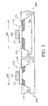
- FIGS. 1 to 5 are cross-section views illustrating an embodiment of the method for fabricating the semiconductor device.
- FIG. 6 illustrates a method for fabricating the photomask 500 .
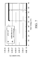
- FIG. 7 illustrates the breakdown voltage of the semiconductor device as known in prior art and one embodiment of the semiconductor device of the invention.
- Embodiments of the present invention provide a method for forming a semiconductor device. References will be made in detail to the present embodiments, examples of which are illustrated in the accompanying drawings. Wherever possible, the same reference numbers are used in the drawings and the descriptions to refer to the same or like parts. In the drawings, the shape and thickness of one embodiment may be exaggerated for clarity and convenience. The descriptions will be directed in particular to elements forming a part of, or cooperating more directly with, apparatus in accordance with the present invention. It is to be understood that elements not specifically shown or described may take various forms well known to those skilled in the art. Further, when a layer is referred to as being on another layer or “on” a substrate, it may be directly on the other layer or on the substrate, or intervening layers may also be present.
- FIGS. 1 to 5 are cross-section views illustrating an embodiment of the method for fabricating the semiconductor device.
- a substrate 100 with a P-well formed thereon is provided.
- the substrate 100 may comprise silicon.
- SiGe, silicon on insulator (SOI), or other commonly used semiconductor substrates can be used for the substrate 100 .
- Isolation structures 24 and 74 such as shallow trench isolation structures, are formed in the substrate 100 , and thus a high voltage device area 200 and a low voltage device area 300 are defined.
- the shallow trench isolation structures may be formed by a shallow trench isolation (STI) process comprising steps, such as, etching a trench in the substrate 100 , filling the trench with a dielectric material, such as a high-density plasma oxide, and planarizing by a chemical mechanical polishing (CMP) process.
- STI shallow trench isolation
- CMP chemical mechanical polishing
- isolation structures 24 and 74 can be field oxides formed by a local oxidation of silicon (LOCOS) process.
- LOC local oxidation of silicon
- a photoresist layer 15 a used for a subsequent photolithography process is formed on the substrate 100 .
- a photomask 500 comprising a shielding region 60 is then provided.
- the shielding region 60 may be corresponded to the high voltage device area 200 on the substrate 100 .
- the pattern of the photomask 500 is transferred onto the photoresist layer 15 a on the substrate 100 by a photolithography process using the photomask 500 .
- the layout pattern of the photomask 500 may be obtained by using a Boolean logic operation.
- FIG. 6 illustrates a method for fabricating the photomask 500 .
- an integrated circuit layout database is provided (step S 11 ).
- the layout database may comprise an N-type ion implantation area data and a high voltage device area data.
- the layout database is read and a Boolean logic operation is executed (step S 11 ) to obtain an operation result.
- the layout pattern of the photomask 500 is obtained by using the operation result (step S 12 ), and the photomask 500 is fabricated by using the layout pattern (step S 13 ).
- the photoresist layer 15 a is patterned to form a patterned photoresist layer 15 b only covering the high voltage device area 200 .
- a P-type ion field 20 a is formed in the low voltage device area 300 outside of the high-voltage device area 200 by a field implantation 20 of a high-density of P-type ions in the substrate 100 using the patterned photoresist layer 15 b as a mask.
- the P-type ion field 20 a is only formed in the low voltage device area 300 , and is not formed in the high voltage device area 200 .
- a distance between the P-type ion field 20 a and the high voltage device area 200 is not less than 0.5 ⁇ m.
- the field implantation 20 is performed with a dosage of P-type ion of about 1E12 ions/cm 2 1 ⁇ E13 ions/cm 2 , such as B+ ions.
- the P-type ion field 20 a can be used for isolation among devices formed in the low voltage device areas 300 later.
- MOS devices 116 are formed on the high voltage device area 200 and the low voltage device areas 300 .
- the MOS devices 116 comprise a source region 123 and a drain region 124 .
- the source region 123 and the drain region 124 may be formed by implantation.
- the MOS devices 116 further comprise a gate electrode 120 and a gate dielectric 121 .
- the gate dielectric 121 may comprise oxide formed by a dry or wet thermal oxidation with an environment including oxide, water, nitric oxide, or combination thereof, or formed by a chemical vapor deposition process using tetraethoxysilane (TEOS) or oxygen as precursor.
- TEOS tetraethoxysilane
- the gate electrode 120 may comprise a conductor material, such as tantalum (Ta), titanium (Ti), molybdenum (Mo), tungsten (W), platinum (Pt), aluminum (Al), hafnium (Hf), or ruthenium (Ru), or metal nitride or metal silicide thereof.
- the gate electrode 120 may comprise polysilicon, such as doped polysilicon or undoped polysilicon formed by a chemical vapor deposition process.
- the gate electrode 120 and the gate dielectric 121 may be patterned by a photolithography process.
- the photolithography process usually comprises forming a photoresist mask by coating a photoresist, and then masking, exposing, and developing the photoresist. As shown in FIG. 5 , after the photoresist mask is patterned, a portion of the gate electrode and the gate dielectric is removed to form the gate electrode 120 and gate dielectric 121 by an etching process.
- the P-type ion field with high dopant concentration is not adjacent to the MOS device 116 on the high voltage device area 200 , thus, leakage occurring in the interface between the MOS device 116 and the high voltage device area 200 is decreased. Therefore, breakdown voltage of the device is improved, and operation voltage range is increased.
- FIG. 7 illustrates the breakdown voltage of the semiconductor device as known in the prior art and one embodiment of the semiconductor device of the invention.
- the breakdown voltage of the semiconductor device as known in the prior art is about 54 V.
- the breakdown voltage of one embodiment of the semiconductor device of the invention is about 76 V.
- the breakdown voltage of embodiments of the semiconductor device of the invention is increased to above about 40% compared to the semiconductor device as known in the prior art.
Landscapes
- Element Separation (AREA)
- Metal-Oxide And Bipolar Metal-Oxide Semiconductor Integrated Circuits (AREA)
Abstract
Description
Claims (8)
Priority Applications (1)
| Application Number | Priority Date | Filing Date | Title |
|---|---|---|---|
| US13/294,945 US9219012B2 (en) | 2008-03-21 | 2011-11-11 | Semiconductor device |
Applications Claiming Priority (3)
| Application Number | Priority Date | Filing Date | Title |
|---|---|---|---|
| TW097110053A TWI358774B (en) | 2008-03-21 | 2008-03-21 | Semiconductor device and fabrication method thereo |
| TWTW97110053 | 2008-03-21 | ||
| TW97110053A | 2008-03-21 |
Related Child Applications (1)
| Application Number | Title | Priority Date | Filing Date |
|---|---|---|---|
| US13/294,945 Division US9219012B2 (en) | 2008-03-21 | 2011-11-11 | Semiconductor device |
Publications (2)
| Publication Number | Publication Date |
|---|---|
| US20090236681A1 US20090236681A1 (en) | 2009-09-24 |
| US8080455B2 true US8080455B2 (en) | 2011-12-20 |
Family
ID=41088018
Family Applications (2)
| Application Number | Title | Priority Date | Filing Date |
|---|---|---|---|
| US12/177,779 Active 2030-03-09 US8080455B2 (en) | 2008-03-21 | 2008-07-22 | Method for fabricating semiconductor device with increased breakdown voltage |
| US13/294,945 Active 2029-05-30 US9219012B2 (en) | 2008-03-21 | 2011-11-11 | Semiconductor device |
Family Applications After (1)
| Application Number | Title | Priority Date | Filing Date |
|---|---|---|---|
| US13/294,945 Active 2029-05-30 US9219012B2 (en) | 2008-03-21 | 2011-11-11 | Semiconductor device |
Country Status (2)
| Country | Link |
|---|---|
| US (2) | US8080455B2 (en) |
| TW (1) | TWI358774B (en) |
Families Citing this family (4)
| Publication number | Priority date | Publication date | Assignee | Title |
|---|---|---|---|---|
| TWI626712B (en) * | 2016-08-25 | 2018-06-11 | 世界先進積體電路股份有限公司 | Semiconductor devices and methods for forming the isolation structure in the semiconductor device |
| US9997410B1 (en) | 2016-11-29 | 2018-06-12 | Vanguard International Semiconductor Corporation | Methods for forming the isolation structure of the semiconductor device and semiconductor devices |
| TWI682540B (en) * | 2018-07-24 | 2020-01-11 | 新唐科技股份有限公司 | Semiconductor device and method for forming the same |
| CN113257804B (en) * | 2020-02-13 | 2022-06-24 | 联芯集成电路制造(厦门)有限公司 | Method for manufacturing semiconductor device |
Citations (3)
| Publication number | Priority date | Publication date | Assignee | Title |
|---|---|---|---|---|
| US6596656B2 (en) * | 2000-10-27 | 2003-07-22 | Hitachi, Ltd. | Manufacturing use of photomasks with an opaque pattern comprising an organic layer photoabsorptive to exposure light with wavelengths exceeding 200 NM |
| CN1701442A (en) | 2003-04-10 | 2005-11-23 | 富士通株式会社 | Semiconductor device and its manufacture method |
| US20060223269A1 (en) * | 2005-03-29 | 2006-10-05 | Oki Electric Industry Co., Ltd. | Method of manufacturing semiconductor device |
Family Cites Families (3)
| Publication number | Priority date | Publication date | Assignee | Title |
|---|---|---|---|---|
| US7067365B1 (en) * | 2005-05-26 | 2006-06-27 | United Microelectronics Corp. | High-voltage metal-oxide-semiconductor devices and method of making the same |
| KR100690924B1 (en) * | 2005-12-21 | 2007-03-09 | 삼성전자주식회사 | Semiconductor integrated circuit device and its manufacturing method |
| US20080073745A1 (en) * | 2006-09-25 | 2008-03-27 | Chien-Shao Tang | High-voltage MOS device improvement by forming implantation regions |
-
2008
- 2008-03-21 TW TW097110053A patent/TWI358774B/en active
- 2008-07-22 US US12/177,779 patent/US8080455B2/en active Active
-
2011
- 2011-11-11 US US13/294,945 patent/US9219012B2/en active Active
Patent Citations (3)
| Publication number | Priority date | Publication date | Assignee | Title |
|---|---|---|---|---|
| US6596656B2 (en) * | 2000-10-27 | 2003-07-22 | Hitachi, Ltd. | Manufacturing use of photomasks with an opaque pattern comprising an organic layer photoabsorptive to exposure light with wavelengths exceeding 200 NM |
| CN1701442A (en) | 2003-04-10 | 2005-11-23 | 富士通株式会社 | Semiconductor device and its manufacture method |
| US20060223269A1 (en) * | 2005-03-29 | 2006-10-05 | Oki Electric Industry Co., Ltd. | Method of manufacturing semiconductor device |
Also Published As
| Publication number | Publication date |
|---|---|
| US9219012B2 (en) | 2015-12-22 |
| TW200941589A (en) | 2009-10-01 |
| TWI358774B (en) | 2012-02-21 |
| US20120056295A1 (en) | 2012-03-08 |
| US20090236681A1 (en) | 2009-09-24 |
Similar Documents
| Publication | Publication Date | Title |
|---|---|---|
| JP4430669B2 (en) | Method of manufacturing a transistor having an asymmetric conductive spacer | |
| US8685818B2 (en) | Method of forming a shallow trench isolation embedded polysilicon resistor | |
| US8053309B2 (en) | Methods of fabricating semiconductor devices | |
| KR102068395B1 (en) | Semiconductor Device Structure having Low Rdson and Manufacturing Method thereof | |
| US8241985B2 (en) | Semiconductor device having gate electrode with lower impurity concentration at edge portions than above channel and method of manufacturing the same | |
| US6262459B1 (en) | High-voltage device and method for manufacturing high-voltage device | |
| TW201909426A (en) | High-voltage transistor using buried insulating layer as gate dielectric | |
| US20050205926A1 (en) | High-voltage MOS transistor and method for fabricating the same | |
| US9219012B2 (en) | Semiconductor device | |
| US7485925B2 (en) | High voltage metal oxide semiconductor transistor and fabricating method thereof | |
| US8063439B2 (en) | Semiconductor device and fabrication method thereof | |
| US20090224327A1 (en) | Plane mos and the method for making the same | |
| US7588978B2 (en) | Method for forming semiconductor device | |
| JP2010177342A (en) | Semiconductor device and manufacturing method therefor | |
| CN113241345A (en) | Semiconductor device structure and forming method thereof | |
| US7273787B2 (en) | Method for manufacturing gate dielectric layer | |
| US20110081760A1 (en) | Method of manufacturing lateral diffusion metal oxide semiconductor device | |
| US7465623B2 (en) | Methods for fabricating a semiconductor device on an SOI substrate | |
| CN101552235B (en) | Semiconductor device and manufacturing method thereof | |
| CN101552228B (en) | Manufacturing method of semiconductor device | |
| KR101035578B1 (en) | Method of manufacturing semiconductor device | |
| US7943461B2 (en) | High-voltage semiconductor device and method for manufacturing the same | |
| JP2927122B2 (en) | Method for manufacturing asymmetric LDD type MOSFET | |
| CN101556921B (en) | Semiconductor device and manufacturing method thereof | |
| TW434794B (en) | Shallow trench isolation structure with shielding effect and the manufacturing method of the same |
Legal Events
| Date | Code | Title | Description |
|---|---|---|---|
| AS | Assignment |
Owner name: VANGUARD INTERNATIONAL SEMICONDUCTOR CORPORATION, Free format text: ASSIGNMENT OF ASSIGNORS INTEREST;ASSIGNORS:LIN, CHIH-PING;CHUANG, PI-KUANG;CHANG, HUNG-LI;AND OTHERS;REEL/FRAME:021297/0802 Effective date: 20080708 |
|
| STCF | Information on status: patent grant |
Free format text: PATENTED CASE |
|
| FPAY | Fee payment |
Year of fee payment: 4 |
|
| MAFP | Maintenance fee payment |
Free format text: PAYMENT OF MAINTENANCE FEE, 8TH YEAR, LARGE ENTITY (ORIGINAL EVENT CODE: M1552); ENTITY STATUS OF PATENT OWNER: LARGE ENTITY Year of fee payment: 8 |
|
| MAFP | Maintenance fee payment |
Free format text: PAYMENT OF MAINTENANCE FEE, 12TH YEAR, LARGE ENTITY (ORIGINAL EVENT CODE: M1553); ENTITY STATUS OF PATENT OWNER: LARGE ENTITY Year of fee payment: 12 |