US8063494B2 - Semiconductor device and power supply unit utilizing the same - Google Patents
Semiconductor device and power supply unit utilizing the same Download PDFInfo
- Publication number
- US8063494B2 US8063494B2 US11/172,679 US17267905A US8063494B2 US 8063494 B2 US8063494 B2 US 8063494B2 US 17267905 A US17267905 A US 17267905A US 8063494 B2 US8063494 B2 US 8063494B2
- Authority
- US
- United States
- Prior art keywords
- terminals
- grid array
- power supply
- supply unit
- switch circuit
- Prior art date
- Legal status (The legal status is an assumption and is not a legal conclusion. Google has not performed a legal analysis and makes no representation as to the accuracy of the status listed.)
- Active, expires
Links
Images


Classifications
-
- H—ELECTRICITY
- H02—GENERATION; CONVERSION OR DISTRIBUTION OF ELECTRIC POWER
- H02M—APPARATUS FOR CONVERSION BETWEEN AC AND AC, BETWEEN AC AND DC, OR BETWEEN DC AND DC, AND FOR USE WITH MAINS OR SIMILAR POWER SUPPLY SYSTEMS; CONVERSION OF DC OR AC INPUT POWER INTO SURGE OUTPUT POWER; CONTROL OR REGULATION THEREOF
- H02M3/00—Conversion of DC power input into DC power output
- H02M3/02—Conversion of DC power input into DC power output without intermediate conversion into AC
- H02M3/04—Conversion of DC power input into DC power output without intermediate conversion into AC by static converters
- H02M3/10—Conversion of DC power input into DC power output without intermediate conversion into AC by static converters using discharge tubes with control electrode or semiconductor devices with control electrode
- H02M3/145—Conversion of DC power input into DC power output without intermediate conversion into AC by static converters using discharge tubes with control electrode or semiconductor devices with control electrode using devices of a triode or transistor type requiring continuous application of a control signal
- H02M3/155—Conversion of DC power input into DC power output without intermediate conversion into AC by static converters using discharge tubes with control electrode or semiconductor devices with control electrode using devices of a triode or transistor type requiring continuous application of a control signal using semiconductor devices only
- H02M3/156—Conversion of DC power input into DC power output without intermediate conversion into AC by static converters using discharge tubes with control electrode or semiconductor devices with control electrode using devices of a triode or transistor type requiring continuous application of a control signal using semiconductor devices only with automatic control of output voltage or current, e.g. switching regulators
- H02M3/158—Conversion of DC power input into DC power output without intermediate conversion into AC by static converters using discharge tubes with control electrode or semiconductor devices with control electrode using devices of a triode or transistor type requiring continuous application of a control signal using semiconductor devices only with automatic control of output voltage or current, e.g. switching regulators including plural semiconductor devices as final control devices for a single load
-
- H—ELECTRICITY
- H10—SEMICONDUCTOR DEVICES; ELECTRIC SOLID-STATE DEVICES NOT OTHERWISE PROVIDED FOR
- H10D—INORGANIC ELECTRIC SEMICONDUCTOR DEVICES
- H10D84/00—Integrated devices formed in or on semiconductor substrates that comprise only semiconducting layers, e.g. on Si wafers or on GaAs-on-Si wafers
-
- H—ELECTRICITY
- H02—GENERATION; CONVERSION OR DISTRIBUTION OF ELECTRIC POWER
- H02M—APPARATUS FOR CONVERSION BETWEEN AC AND AC, BETWEEN AC AND DC, OR BETWEEN DC AND DC, AND FOR USE WITH MAINS OR SIMILAR POWER SUPPLY SYSTEMS; CONVERSION OF DC OR AC INPUT POWER INTO SURGE OUTPUT POWER; CONTROL OR REGULATION THEREOF
- H02M3/00—Conversion of DC power input into DC power output
- H02M3/02—Conversion of DC power input into DC power output without intermediate conversion into AC
- H02M3/04—Conversion of DC power input into DC power output without intermediate conversion into AC by static converters
- H02M3/10—Conversion of DC power input into DC power output without intermediate conversion into AC by static converters using discharge tubes with control electrode or semiconductor devices with control electrode
- H02M3/145—Conversion of DC power input into DC power output without intermediate conversion into AC by static converters using discharge tubes with control electrode or semiconductor devices with control electrode using devices of a triode or transistor type requiring continuous application of a control signal
- H02M3/155—Conversion of DC power input into DC power output without intermediate conversion into AC by static converters using discharge tubes with control electrode or semiconductor devices with control electrode using devices of a triode or transistor type requiring continuous application of a control signal using semiconductor devices only
-
- H—ELECTRICITY
- H10—SEMICONDUCTOR DEVICES; ELECTRIC SOLID-STATE DEVICES NOT OTHERWISE PROVIDED FOR
- H10W—GENERIC PACKAGES, INTERCONNECTIONS, CONNECTORS OR OTHER CONSTRUCTIONAL DETAILS OF DEVICES COVERED BY CLASS H10
- H10W72/00—Interconnections or connectors in packages
- H10W72/20—Bump connectors, e.g. solder bumps or copper pillars; Dummy bumps; Thermal bumps
- H10W72/231—Shapes
- H10W72/232—Plan-view shape, i.e. in top view
-
- H—ELECTRICITY
- H10—SEMICONDUCTOR DEVICES; ELECTRIC SOLID-STATE DEVICES NOT OTHERWISE PROVIDED FOR
- H10W—GENERIC PACKAGES, INTERCONNECTIONS, CONNECTORS OR OTHER CONSTRUCTIONAL DETAILS OF DEVICES COVERED BY CLASS H10
- H10W72/00—Interconnections or connectors in packages
- H10W72/20—Bump connectors, e.g. solder bumps or copper pillars; Dummy bumps; Thermal bumps
- H10W72/241—Dispositions, e.g. layouts
- H10W72/247—Dispositions of multiple bumps
- H10W72/248—Top-view layouts, e.g. mirror arrays
Definitions
- This invention relates to a semiconductor device having built-in switching transistors, and a power supply unit utilizing such semiconductor device.
- switching power supply units having an integrated semiconductor circuit that includes a switching element (e.g. transistor switch) and a drive circuit controlling the switching element to control the output voltage of the switching power supply unit.
- a switching element e.g. transistor switch
- FIG. 3 shows a circuit arrangement of a conventional switching power supply unit, in which a semiconductor integrated circuit (IC) 10 has a transistor switch Qo and a drive circuit 20 for driving the transistor switch Qo.
- This transistor switch Qo is directly connected in series to a coil Lo via a pad Po of the IC 10 .
- the voltage appearing at the node of the pad Po and the coil Lo is rectified and smoothed by a diode Do and a capacitor Co to provide a dc output voltage Vout.
- switching current Io is supplied from a power supply (e.g. a battery) having an input voltage Vin to the transistor switch Qo via the coil Lo and the pad Po, and the transistor switch Qo.
- the current Io grows larger with time after the transistor switch Qo is turned on. If the transistor switch Qo is turned off, the energy accumulated in the coil Lo is liberated therefrom, which is rectified and smoothed by the diode Do and the capacitor Co before it is provided as the output voltage Vout of the power supply unit, converted from the input voltage Vin.
- the magnitude of the output voltage Vout is determined by the duty ratio Ton/(Ton+Toff) of ON time Ton to OFF time Toff of the transistor switch Qo.
- the duty ratio is controlled by feeding the drive circuit 20 a feedback voltage indicative of the output voltage Vout in such a way that the feedback voltage equilibrate with a predetermined reference voltage, thereby holding the output voltage Vout at a predetermined level.
- multiple bonding wires can be parallelly connected to the terminal (see, for example, Japanese Patent Applications Laid Open No. H7-202097 and No. 2000-114307).
- a wafer-level chip-sized package (WL-CSP) type IC has been increasingly adopted for miniaturization of the IC.
- a WL-CSP type IC has pluralities of ball-shaped terminals (hereinafter referred to as ball terminals) arranged in a two-dimensional grid array structure (the terminals in the structure referred to as ball grid array (BGA) terminals) to establish electric connections with external circuits.
- BGA ball grid array
- Each of the ball terminals is made very small in order to attain a high terminal density in the IC package.
- the current Io has a comparatively large magnitude since it pertains to the switching of a transistor switch, so that it can exceed the withstand current level (or permissible current level) of one ball terminal.
- the ball terminal connected to a semiconductor switch generates heat determined by the contact resistance thereof and the current Io. As a consequence, these ball terminals connected to a transistor switch are in jeopardy of being melt down by heat.
- a semiconductor device equipped with a switch circuit and a drive circuit for performing ON-OFF control of the switch circuit and having grid array terminals forming a grid array structure, wherein the output end of the switch circuit is connected to multiple terminals of the grid array structure. These multiple terminals may be called as switching output terminals.
- Each pair of nearest neighbors of the multiple terminals may be provided therebetween with at least one interposing terminal other than the multiple terminals.
- the multiple terminals may be all located at the outermost peripheral terminal positions of the grid array structure.
- the switch circuit may consist of a multiplicity of transistor switches connected in parallel with one another so as to be simultaneously turned on and off.
- Each of the grid array terminals may be a ball-shaped terminal.
- a power supply unit equipped with a semiconductor device that includes a switch circuit and a drive circuit for performing ON-OFF control of the switch circuit and has grid array terminals forming a grid array structure, wherein
- the output end of the switch circuit is connected to multiple terminals of the grid array structure
- the multiple terminals are connected with one another outside the semiconductor device.
- the power supply unit is adapted to convert its input voltage into an output voltage under the ON-OFF control of the switch circuit.
- the output end of the switch circuit is connected to multiple terminals of the grid array structure.
- current that flows through any one grid array terminal is reduced to or less than a permissible level, so that Joule heat due to the contact resistance between the terminal and an IC socket is reduced, thereby suppressing hazardous melting of the grid array terminal.
- each pair of nearest neighbors of the multiple terminals is provided with at least one interposing terminal through which no or little current flows, a distributed heat dissipative area is provided for the terminals. Thus, Joule heat is easily dissipated, and temperature rise in these terminals is suppressed. Since all the multiple terminals are located at the outermost peripheral terminal positions of the grid array structure, thicker, and hence less resistive, external wires can be connected to the multiple terminals, which facilitates enhanced heat radiation.
- FIG. 1 shows a circuit arrangement of an IC in accordance with one embodiment of the invention and an inventive power supply unit utilizing the IC.
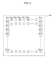
- FIG. 2 shows a BGA structure of terminals on one side of the IC of FIG. 1 .
- FIG. 3 shows a circuit arrangement of a conventional switching power supply unit.
- FIG. 1 there is shown schematically an IC 10 A in accordance with one embodiment of the invention and a power supply unit utilizing the IC 10 A.
- the IC 10 A includes an IC chip 11 A.
- FIG. 2 shows a ball grid array (BGA) structure in which pluralities of ball terminals are arranged in a lattice configuration on one side of the IC 10 A.
- BGA ball grid array
- Symbols Lo, Do, Co, Vin, and Vout of FIG. 3 respectively refer to a coil, a diode, a capacitor, an input voltage, and an output voltage, as in FIG. 1 .
- the IC 10 A is a WL-CSP type IC having a reduced size.
- the IC 10 A is a WL-CSP type IC having a reduced size.
- Formed on one side (e.g. backside) of the IC 10 A is a BGA structure of ball terminals B 1 - 1 -Bn-m arrayed in m rows and n columns, as shown in FIG. 2 .
- a switch circuit consisting of transistor switches Q 1 -Q 3 , and a drive circuit 20 for driving these transistor switches Q 1 -Q 3 , all formed in the IC 10 A.
- the transistor switches Q 1 -Q 3 of the example shown herein are NPN bipolar transistors, they can be of another type of transistors such as MOSFETs for example. These transistor switches Q 1 -Q 3 are simultaneously switched on and off by an ON-OFF drive signal issued from the drive circuit 20 .
- the switch circuit is shown having three transistor switches Q 1 -Q 3 , but it may have only one transistor switch. However, from the point of preventing the switch circuit from being influenced by breaking of wires and/or loose connection of terminals, it is preferred to provide the switch circuit with at least two transistor switches. Furthermore, if the switch circuit has more than one transistor switch, it has extra current drive capability.
- the collectors of the transistor switches Q 1 -Q 3 are respectively connected to multiple ball terminals B 2 - 1 , B 4 - 1 , and B 6 - 1 belonging to the BGA terminals B 1 - 1 -Bn-m via the respective pads P 2 - 1 , P 4 - 1 , P 6 - 1 of the IC chip 11 A and the bumps associated with the pads. These collectors are preferably connected with one another.
- the multiple ball terminals B 2 - 1 , B 4 - 1 , and B 6 - 1 to which the respective collectors of the transistor switches Q 1 -Q 3 are connected are also connected to one another outside the IC 10 A.
- the multiple ball terminals B 2 - 1 , B 4 - 1 , and B 6 - 1 coupled together are connected to the node of the coil Lo and the diode Do.
- the transistor switches Q 1 -Q 3 are turned on, the current Io flowing through the coil Lo increases with time.
- the current Io is shunted evenly to the multiple ball terminals B 2 - 1 , B 4 - 1 , and B 6 - 1 , thereby providing each of the transistor switches Q 1 -Q 3 with current of about Io/3.
- the output voltage Vout may be controlled in the same manner as conventional, as described in connection with FIG. 3 .
- This arrangement permits the shunted current to each of the parallelly connected multiple ball terminals B 2 - 1 , B 4 - 1 , and B 6 - 1 to be reduced to or below a permissible level, and causes the Joule heat due to the contact resistance of the IC 10 A with the substrate to be sufficiently reduced. Accordingly, hazardous melting of the ball terminals of the BGA structure can be avoided.
- the switch circuit is little influenced by breaking of wires and/or loose contact of the pads if it happens, due to the fact that the multiple ball terminals B 2 - 1 , B 4 - 1 , and B 6 - 1 are parallelly connected and so are the switching transistors Q 1 -Q 3 .
- each pair of nearest neighbors of the multiple ball terminals B 2 - 1 , B 4 - 1 , and B 6 - 1 is provided therebetween at least one interposing ball terminal B 3 - 1 and B 5 - 1 other than the multiple ball terminals. It should be understood that there can be more than one interposing ball terminal between each pair of nearest neighbors of the multiple ball terminals B 2 - 1 , B 4 - 1 , and B 6 - 1 .
- interposing ball terminals are terminals through which flows no or an extremely small amount of current (e.g. Io/10) as compared with the current (Io/3) flowing through the multiple ball terminals B 2 - 1 , B 4 - 1 , and B 6 - 1 .
- All the multiple ball terminals B 2 - 1 , B 4 - 1 , and B 6 - 1 are located at the outermost peripheral terminal positions of the BGA configuration.
- external wiring leads connected to these terminals can be made thicker to reduce their electric resistances and enhance their heat-dissipative power as compared with those connected to terminals located at inner terminal positions of the BGA structure.
- the invention has been described with a particular reference to a BGA structure, the invention is not limited to the example as described and shown above.
- the invention contemplates an IC having a pin gripped array (PGA) structure in which pluralities of pin-shaped terminals are arranged in a lattice configuration on one side of the IC.
- PGA pin gripped array
- the invention can be applied to a wide range of switching power supply units utilizing a switching circuit, including a step-up dc-dc conversion type power supply unit as shown in FIG. 1 , a step-down dc-dc conversion type power supply unit and a step-down dc-ac conversion type power supply unit.
- the invention can be also applied to motor drivers utilizing a switch circuit.
Landscapes
- Engineering & Computer Science (AREA)
- Power Engineering (AREA)
- Semiconductor Integrated Circuits (AREA)
- Dc-Dc Converters (AREA)
- Design And Manufacture Of Integrated Circuits (AREA)
- Multi-Conductor Connections (AREA)
Abstract
Description
Claims (5)
Priority Applications (4)
| Application Number | Priority Date | Filing Date | Title |
|---|---|---|---|
| US13/253,805 US8704357B2 (en) | 2004-07-21 | 2011-10-05 | Semiconductor device and power supply unit utilizing the same |
| US14/191,242 US8872577B2 (en) | 2004-07-21 | 2014-02-26 | Semiconductor device and power supply unit utilizing the same |
| US14/494,335 US9391038B2 (en) | 2004-07-21 | 2014-09-23 | Semiconductor device and power supply unit utilizing the same |
| US15/182,500 US9812964B2 (en) | 2004-07-21 | 2016-06-14 | Semiconductor device and power supply unit utilizing the same |
Applications Claiming Priority (2)
| Application Number | Priority Date | Filing Date | Title |
|---|---|---|---|
| JP2004-212749 | 2004-07-21 | ||
| JP2004212749A JP4591886B2 (en) | 2004-07-21 | 2004-07-21 | Power supply circuit device using semiconductor device |
Related Child Applications (1)
| Application Number | Title | Priority Date | Filing Date |
|---|---|---|---|
| US13/253,805 Division US8704357B2 (en) | 2004-07-21 | 2011-10-05 | Semiconductor device and power supply unit utilizing the same |
Publications (2)
| Publication Number | Publication Date |
|---|---|
| US20060017067A1 US20060017067A1 (en) | 2006-01-26 |
| US8063494B2 true US8063494B2 (en) | 2011-11-22 |
Family
ID=35656207
Family Applications (5)
| Application Number | Title | Priority Date | Filing Date |
|---|---|---|---|
| US11/172,679 Active 2026-07-03 US8063494B2 (en) | 2004-07-21 | 2005-06-30 | Semiconductor device and power supply unit utilizing the same |
| US13/253,805 Active 2026-05-27 US8704357B2 (en) | 2004-07-21 | 2011-10-05 | Semiconductor device and power supply unit utilizing the same |
| US14/191,242 Expired - Lifetime US8872577B2 (en) | 2004-07-21 | 2014-02-26 | Semiconductor device and power supply unit utilizing the same |
| US14/494,335 Expired - Lifetime US9391038B2 (en) | 2004-07-21 | 2014-09-23 | Semiconductor device and power supply unit utilizing the same |
| US15/182,500 Expired - Fee Related US9812964B2 (en) | 2004-07-21 | 2016-06-14 | Semiconductor device and power supply unit utilizing the same |
Family Applications After (4)
| Application Number | Title | Priority Date | Filing Date |
|---|---|---|---|
| US13/253,805 Active 2026-05-27 US8704357B2 (en) | 2004-07-21 | 2011-10-05 | Semiconductor device and power supply unit utilizing the same |
| US14/191,242 Expired - Lifetime US8872577B2 (en) | 2004-07-21 | 2014-02-26 | Semiconductor device and power supply unit utilizing the same |
| US14/494,335 Expired - Lifetime US9391038B2 (en) | 2004-07-21 | 2014-09-23 | Semiconductor device and power supply unit utilizing the same |
| US15/182,500 Expired - Fee Related US9812964B2 (en) | 2004-07-21 | 2016-06-14 | Semiconductor device and power supply unit utilizing the same |
Country Status (5)
| Country | Link |
|---|---|
| US (5) | US8063494B2 (en) |
| JP (1) | JP4591886B2 (en) |
| KR (1) | KR20060048558A (en) |
| CN (2) | CN100485916C (en) |
| TW (1) | TWI380344B (en) |
Cited By (3)
| Publication number | Priority date | Publication date | Assignee | Title |
|---|---|---|---|---|
| US20120032713A1 (en) * | 2004-07-21 | 2012-02-09 | Rohm Co., Ltd. | Semiconductor Device and Power Supply Unit Utilizing the Same |
| US20120173030A1 (en) * | 2009-02-11 | 2012-07-05 | Accenture Global Services Limited | Method and system for reducing feeder circuit loss using demand response |
| US20120176193A1 (en) * | 2011-01-10 | 2012-07-12 | Taiwan Semiconductor Manufacturing Company, Ltd. | Driver for a semiconductor chip |
Families Citing this family (7)
| Publication number | Priority date | Publication date | Assignee | Title |
|---|---|---|---|---|
| US8008897B2 (en) * | 2007-06-11 | 2011-08-30 | Alpha & Omega Semiconductor, Ltd | Boost converter with integrated high power discrete FET and low voltage controller |
| JP2008124367A (en) * | 2006-11-15 | 2008-05-29 | Univ Of Tsukuba | Integrated circuit device and method of using the same |
| US8456141B2 (en) | 2007-06-11 | 2013-06-04 | Alpha & Omega Semiconductor, Inc. | Boost converter with integrated high power discrete FET and low voltage controller |
| KR101387922B1 (en) * | 2007-07-24 | 2014-04-22 | 삼성디스플레이 주식회사 | Driver ic, driver ic package having the same and display apparatus having the driver ic package |
| JP5923929B2 (en) * | 2011-10-27 | 2016-05-25 | ソニー株式会社 | Solid-state imaging device and camera system |
| CN111868537B (en) * | 2018-03-12 | 2023-12-05 | 罗姆股份有限公司 | Semiconductor device and identification method of semiconductor device |
| CN111037586B (en) * | 2019-12-27 | 2025-02-18 | 深圳市越疆科技股份有限公司 | Multi-component systems and robotic equipment |
Citations (9)
| Publication number | Priority date | Publication date | Assignee | Title |
|---|---|---|---|---|
| JPH07202097A (en) | 1994-01-11 | 1995-08-04 | Hitachi Ltd | Semiconductor device and lead frame |
| US5805124A (en) * | 1996-04-04 | 1998-09-08 | Norhtrop Grumman Corporation | Symmetric row drive for an electroluminescent display |
| US6037745A (en) * | 1997-07-03 | 2000-03-14 | Kabushiki Kaisha Toyoda Jidoshokki | Battery charger with monitor and protection circuits |
| JP2000114307A (en) | 1998-10-08 | 2000-04-21 | Nec Kansai Ltd | Semiconductor device |
| JP2003203982A (en) | 2002-01-08 | 2003-07-18 | Ricoh Co Ltd | Semiconductor device, method of manufacturing the same, and DC-DC converter |
| JP2003282622A (en) | 2002-03-25 | 2003-10-03 | Toshiba Corp | Semiconductor device |
| US20040023450A1 (en) * | 2001-02-08 | 2004-02-05 | Mitsuaki Katagiri | Semiconductor integrated circuit device and its manufacturing method |
| US20040061220A1 (en) * | 1996-03-22 | 2004-04-01 | Chuichi Miyazaki | Semiconductor device and manufacturing method thereof |
| US20040227666A1 (en) * | 2003-02-26 | 2004-11-18 | Masakazu Adachi | Antenna switch module, all-in-one communication module, communication apparatus and method for manufacturing antenna switch module |
Family Cites Families (8)
| Publication number | Priority date | Publication date | Assignee | Title |
|---|---|---|---|---|
| CN2133970Y (en) * | 1992-05-23 | 1993-05-19 | 李林山 | Phase interruption and overload protector for power transformer and motor |
| JP3294490B2 (en) * | 1995-11-29 | 2002-06-24 | 株式会社日立製作所 | BGA type semiconductor device |
| CN1284421C (en) * | 2000-03-22 | 2006-11-08 | 国际整流器公司 | Gate driver multi-chip module |
| US6650015B2 (en) * | 2002-02-05 | 2003-11-18 | Siliconware Precision Industries Co., Ltd. | Cavity-down ball grid array package with semiconductor chip solder ball |
| JP2003324183A (en) * | 2002-05-07 | 2003-11-14 | Mitsubishi Electric Corp | Semiconductor device |
| JP4591886B2 (en) * | 2004-07-21 | 2010-12-01 | ローム株式会社 | Power supply circuit device using semiconductor device |
| US8830711B2 (en) * | 2010-08-10 | 2014-09-09 | Virginia Tech Intellectual Properties, Inc. | Hybrid switch for resonant power converters |
| JP5863599B2 (en) * | 2012-08-21 | 2016-02-16 | 三菱電機株式会社 | Power module |
-
2004
- 2004-07-21 JP JP2004212749A patent/JP4591886B2/en not_active Expired - Lifetime
-
2005
- 2005-06-27 KR KR1020050055764A patent/KR20060048558A/en not_active Withdrawn
- 2005-06-29 TW TW094121805A patent/TWI380344B/en not_active IP Right Cessation
- 2005-06-30 US US11/172,679 patent/US8063494B2/en active Active
- 2005-07-19 CN CNB2005100860530A patent/CN100485916C/en not_active Expired - Lifetime
- 2005-07-19 CN CN200910128938.0A patent/CN101562166B/en not_active Expired - Lifetime
-
2011
- 2011-10-05 US US13/253,805 patent/US8704357B2/en active Active
-
2014
- 2014-02-26 US US14/191,242 patent/US8872577B2/en not_active Expired - Lifetime
- 2014-09-23 US US14/494,335 patent/US9391038B2/en not_active Expired - Lifetime
-
2016
- 2016-06-14 US US15/182,500 patent/US9812964B2/en not_active Expired - Fee Related
Patent Citations (12)
| Publication number | Priority date | Publication date | Assignee | Title |
|---|---|---|---|---|
| JPH07202097A (en) | 1994-01-11 | 1995-08-04 | Hitachi Ltd | Semiconductor device and lead frame |
| US20040061220A1 (en) * | 1996-03-22 | 2004-04-01 | Chuichi Miyazaki | Semiconductor device and manufacturing method thereof |
| US5805124A (en) * | 1996-04-04 | 1998-09-08 | Norhtrop Grumman Corporation | Symmetric row drive for an electroluminescent display |
| US6037745A (en) * | 1997-07-03 | 2000-03-14 | Kabushiki Kaisha Toyoda Jidoshokki | Battery charger with monitor and protection circuits |
| JP2000114307A (en) | 1998-10-08 | 2000-04-21 | Nec Kansai Ltd | Semiconductor device |
| US20040023450A1 (en) * | 2001-02-08 | 2004-02-05 | Mitsuaki Katagiri | Semiconductor integrated circuit device and its manufacturing method |
| JP2003203982A (en) | 2002-01-08 | 2003-07-18 | Ricoh Co Ltd | Semiconductor device, method of manufacturing the same, and DC-DC converter |
| US20030141529A1 (en) | 2002-01-08 | 2003-07-31 | Masami Seto | Semiconductor apparatus having a built-in-electric coil and a method of making the semiconductor apparatus |
| US6977403B2 (en) | 2002-01-08 | 2005-12-20 | Ricoh Company, Ltd. | Semiconductor apparatus having a built-in-electric coil and a method of making the semiconductor apparatus |
| US7081659B2 (en) | 2002-01-08 | 2006-07-25 | Ricoh Company, Ltd. | Semiconductor apparatus having a built-in electric coil and a method of making the semiconductor apparatus |
| JP2003282622A (en) | 2002-03-25 | 2003-10-03 | Toshiba Corp | Semiconductor device |
| US20040227666A1 (en) * | 2003-02-26 | 2004-11-18 | Masakazu Adachi | Antenna switch module, all-in-one communication module, communication apparatus and method for manufacturing antenna switch module |
Cited By (10)
| Publication number | Priority date | Publication date | Assignee | Title |
|---|---|---|---|---|
| US20120032713A1 (en) * | 2004-07-21 | 2012-02-09 | Rohm Co., Ltd. | Semiconductor Device and Power Supply Unit Utilizing the Same |
| US8704357B2 (en) * | 2004-07-21 | 2014-04-22 | Rohm Co., Ltd. | Semiconductor device and power supply unit utilizing the same |
| US20140175648A1 (en) * | 2004-07-21 | 2014-06-26 | Rohm Co., Ltd. | Semiconductor Device and Power Supply Unit Utilizing the Same |
| US8872577B2 (en) * | 2004-07-21 | 2014-10-28 | Rohm Co., Ltd. | Semiconductor device and power supply unit utilizing the same |
| US9391038B2 (en) | 2004-07-21 | 2016-07-12 | Rohm Co., Ltd. | Semiconductor device and power supply unit utilizing the same |
| US9812964B2 (en) | 2004-07-21 | 2017-11-07 | Rohm Co., Ltd. | Semiconductor device and power supply unit utilizing the same |
| US20120173030A1 (en) * | 2009-02-11 | 2012-07-05 | Accenture Global Services Limited | Method and system for reducing feeder circuit loss using demand response |
| US8655500B2 (en) * | 2009-02-11 | 2014-02-18 | Accenture Global Services Limited | Method and system for reducing feeder circuit loss using demand response |
| US20120176193A1 (en) * | 2011-01-10 | 2012-07-12 | Taiwan Semiconductor Manufacturing Company, Ltd. | Driver for a semiconductor chip |
| US8378742B2 (en) * | 2011-01-10 | 2013-02-19 | Taiwan Semiconductor Manufacturing Company, Ltd. | Driver for a semiconductor chip |
Also Published As
| Publication number | Publication date |
|---|---|
| US20060017067A1 (en) | 2006-01-26 |
| CN101562166A (en) | 2009-10-21 |
| CN101562166B (en) | 2014-10-22 |
| CN100485916C (en) | 2009-05-06 |
| CN1725484A (en) | 2006-01-25 |
| US9812964B2 (en) | 2017-11-07 |
| US8872577B2 (en) | 2014-10-28 |
| US20160294288A1 (en) | 2016-10-06 |
| JP4591886B2 (en) | 2010-12-01 |
| US20140175648A1 (en) | 2014-06-26 |
| US8704357B2 (en) | 2014-04-22 |
| US9391038B2 (en) | 2016-07-12 |
| TW200605185A (en) | 2006-02-01 |
| KR20060048558A (en) | 2006-05-18 |
| US20120032713A1 (en) | 2012-02-09 |
| US20150021768A1 (en) | 2015-01-22 |
| JP2006032827A (en) | 2006-02-02 |
| TWI380344B (en) | 2012-12-21 |
Similar Documents
| Publication | Publication Date | Title |
|---|---|---|
| US9812964B2 (en) | Semiconductor device and power supply unit utilizing the same | |
| US8237493B2 (en) | Semiconductor device and power supply device using the same | |
| US6713823B1 (en) | Conductive routings in integrated circuits | |
| JP6705393B2 (en) | Semiconductor device and power converter | |
| US20220319976A1 (en) | Three-level power module | |
| WO2012091780A1 (en) | Semiconductor device with stacked power converter | |
| TWI909381B (en) | Reconfigurable power converter | |
| US20090273913A1 (en) | Circuit arrangement having two semiconductor switching elements and one freewheeling element | |
| JP4808979B2 (en) | Multi-chip type semiconductor device and manufacturing method thereof | |
| US7705434B2 (en) | Power semiconductor component having chip stack | |
| WO2017047415A1 (en) | Semiconductor device | |
| JP4697025B2 (en) | Power semiconductor module | |
| US20100127690A1 (en) | Semiconductor apparatus | |
| US20260090417A1 (en) | Package for a power circuit | |
| TWI913612B (en) | Voltage convertor module | |
| JP2580798B2 (en) | Transistor module for power converter | |
| JPH10125938A (en) | Center tap type semiconductor device |
Legal Events
| Date | Code | Title | Description |
|---|---|---|---|
| AS | Assignment |
Owner name: ROHM CO., LTD., JAPAN Free format text: ASSIGNMENT OF ASSIGNORS INTEREST;ASSIGNOR:KITAWAGA, ATSUSHI;REEL/FRAME:016760/0408 Effective date: 20050613 |
|
| AS | Assignment |
Owner name: ROHM CO., LTD., JAPAN Free format text: CORRECTIVE DOCUMENT TO CORRECT ASSIGNOR NAME: ATSUSHI KITAGAWA PREVIOUSLY RECORDED ON REEL: 016760, FRAME 0408;ASSIGNOR:KITAGAWA, ATSUSHI;REEL/FRAME:017382/0254 Effective date: 20050613 Owner name: ROHM CO., LTD., JAPAN Free format text: CORRECTIVE DOCUMENT TO CORRECT ASSIGNOR NAME;ASSIGNOR:KITAGAWA, ATSUSHI;REEL/FRAME:017382/0254 Effective date: 20050613 |
|
| FEPP | Fee payment procedure |
Free format text: PAYER NUMBER DE-ASSIGNED (ORIGINAL EVENT CODE: RMPN); ENTITY STATUS OF PATENT OWNER: LARGE ENTITY |
|
| STCF | Information on status: patent grant |
Free format text: PATENTED CASE |
|
| FPAY | Fee payment |
Year of fee payment: 4 |
|
| MAFP | Maintenance fee payment |
Free format text: PAYMENT OF MAINTENANCE FEE, 8TH YEAR, LARGE ENTITY (ORIGINAL EVENT CODE: M1552); ENTITY STATUS OF PATENT OWNER: LARGE ENTITY Year of fee payment: 8 |
|
| MAFP | Maintenance fee payment |
Free format text: PAYMENT OF MAINTENANCE FEE, 12TH YEAR, LARGE ENTITY (ORIGINAL EVENT CODE: M1553); ENTITY STATUS OF PATENT OWNER: LARGE ENTITY Year of fee payment: 12 |