US8044740B2 - Temperature compensated RC oscillator for signal conditioning ASIC using source bulk voltage of MOSFET - Google Patents
Temperature compensated RC oscillator for signal conditioning ASIC using source bulk voltage of MOSFET Download PDFInfo
- Publication number
- US8044740B2 US8044740B2 US12/553,931 US55393109A US8044740B2 US 8044740 B2 US8044740 B2 US 8044740B2 US 55393109 A US55393109 A US 55393109A US 8044740 B2 US8044740 B2 US 8044740B2
- Authority
- US
- United States
- Prior art keywords
- pmos
- nmos
- source
- current
- nmos device
- Prior art date
- Legal status (The legal status is an assumption and is not a legal conclusion. Google has not performed a legal analysis and makes no representation as to the accuracy of the status listed.)
- Expired - Fee Related, expires
Links
- 230000003750 conditioning effect Effects 0.000 title 1
- 238000013461 design Methods 0.000 abstract description 3
- 239000003990 capacitor Substances 0.000 description 15
- 230000007423 decrease Effects 0.000 description 5
- 230000003247 decreasing effect Effects 0.000 description 5
- 238000010586 diagram Methods 0.000 description 5
- 238000000034 method Methods 0.000 description 5
- 238000013459 approach Methods 0.000 description 2
- 239000013078 crystal Substances 0.000 description 2
- 230000001419 dependent effect Effects 0.000 description 2
- 238000007599 discharging Methods 0.000 description 2
- 230000000630 rising effect Effects 0.000 description 2
- 230000003044 adaptive effect Effects 0.000 description 1
- 230000003321 amplification Effects 0.000 description 1
- 238000004891 communication Methods 0.000 description 1
- 239000000463 material Substances 0.000 description 1
- 238000012986 modification Methods 0.000 description 1
- 230000004048 modification Effects 0.000 description 1
- 238000003199 nucleic acid amplification method Methods 0.000 description 1
- 238000004513 sizing Methods 0.000 description 1
- 230000006641 stabilisation Effects 0.000 description 1
- 238000011105 stabilization Methods 0.000 description 1
- 230000001052 transient effect Effects 0.000 description 1
- 230000001960 triggered effect Effects 0.000 description 1
- 239000002699 waste material Substances 0.000 description 1
Images


Classifications
-
- H—ELECTRICITY
- H03—ELECTRONIC CIRCUITRY
- H03L—AUTOMATIC CONTROL, STARTING, SYNCHRONISATION OR STABILISATION OF GENERATORS OF ELECTRONIC OSCILLATIONS OR PULSES
- H03L1/00—Stabilisation of generator output against variations of physical values, e.g. power supply
- H03L1/02—Stabilisation of generator output against variations of physical values, e.g. power supply against variations of temperature only
- H03L1/022—Stabilisation of generator output against variations of physical values, e.g. power supply against variations of temperature only by indirect stabilisation, i.e. by generating an electrical correction signal which is a function of the temperature
-
- H—ELECTRICITY
- H03—ELECTRONIC CIRCUITRY
- H03K—PULSE TECHNIQUE
- H03K3/00—Circuits for generating electric pulses; Monostable, bistable or multistable circuits
- H03K3/01—Details
- H03K3/011—Modifications of generator to compensate for variations in physical values, e.g. voltage, temperature
-
- H—ELECTRICITY
- H03—ELECTRONIC CIRCUITRY
- H03K—PULSE TECHNIQUE
- H03K3/00—Circuits for generating electric pulses; Monostable, bistable or multistable circuits
- H03K3/02—Generators characterised by the type of circuit or by the means used for producing pulses
- H03K3/027—Generators characterised by the type of circuit or by the means used for producing pulses by the use of logic circuits, with internal or external positive feedback
- H03K3/03—Astable circuits
-
- H—ELECTRICITY
- H03—ELECTRONIC CIRCUITRY
- H03K—PULSE TECHNIQUE
- H03K3/00—Circuits for generating electric pulses; Monostable, bistable or multistable circuits
- H03K3/02—Generators characterised by the type of circuit or by the means used for producing pulses
- H03K3/353—Generators characterised by the type of circuit or by the means used for producing pulses by the use, as active elements, of field-effect transistors with internal or external positive feedback
- H03K3/354—Astable circuits
-
- H—ELECTRICITY
- H03—ELECTRONIC CIRCUITRY
- H03K—PULSE TECHNIQUE
- H03K4/00—Generating pulses having essentially a finite slope or stepped portions
- H03K4/06—Generating pulses having essentially a finite slope or stepped portions having triangular shape
- H03K4/08—Generating pulses having essentially a finite slope or stepped portions having triangular shape having sawtooth shape
- H03K4/48—Generating pulses having essentially a finite slope or stepped portions having triangular shape having sawtooth shape using as active elements semiconductor devices
- H03K4/50—Generating pulses having essentially a finite slope or stepped portions having triangular shape having sawtooth shape using as active elements semiconductor devices in which a sawtooth voltage is produced across a capacitor
- H03K4/501—Generating pulses having essentially a finite slope or stepped portions having triangular shape having sawtooth shape using as active elements semiconductor devices in which a sawtooth voltage is produced across a capacitor the starting point of the flyback period being determined by the amplitude of the voltage across the capacitor, e.g. by a comparator
- H03K4/502—Generating pulses having essentially a finite slope or stepped portions having triangular shape having sawtooth shape using as active elements semiconductor devices in which a sawtooth voltage is produced across a capacitor the starting point of the flyback period being determined by the amplitude of the voltage across the capacitor, e.g. by a comparator the capacitor being charged from a constant-current source
Definitions
- the present invention relates to an RC oscillator and, more particularly, to a temperature-stabilized oscillator with minimal hardware and low power consumption.
- An accurate clock generator is very important for signal-conditioning in a variety of applications.
- An application specific integrated circuit (ASIC) operating that utilizes such a generator in an environment is subject to substantial variations in temperature.
- ASIC application specific integrated circuit
- One example of such an environment is an automotive application, in which the temperature range could be from ⁇ 50 C to 150 C.
- An unstable clock frequency reduces the performance of the internal circuits, especially the switched-cap circuits, baud rate generator and handshake circuits.
- RC oscillators have been studied for a long time.
- Conventional RC oscillators are limited to low-frequency, low-precision applications sources such as tone generators, alarms or flashing indicators.
- the temperature coefficient (TC) parameters of those resistors and capacitors are hard to control.
- RC circuits like canonic RC-active frequency oscillator, require an operational amplifier as disclosed, for example in U.S. Pat. No. 5,870,345 or a comparator as disclosed in US Patent Publication No. 2005/0134393, to stabilize the oscillating frequency.
- an operational amplifier as disclosed, for example in U.S. Pat. No. 5,870,345 or a comparator as disclosed in US Patent Publication No. 2005/0134393, to stabilize the oscillating frequency.
- To provide whether to build a high gain operational amplifier or a high speed comparator is complicated and expensive in the hardware and power consumption. This is particularly true if the frequency of the application is up to megahertz range.
- the offset voltage of the operational amplifier and comparator is temperature dependent, which gives a temperature dependent clock signal. To correct this offset, a complicated circuitry is required.
- a temperature compensated CMOS RC oscillator circuit changes the source-bulk voltage to stabilize the MOSFET's threshold voltage variation over temperature using a resistor and temperature-correlated bias current.
- the MOSFET's source is connected to ground through a resistor. This temperature-correlated bias current also runs through this resistor. When temperature increases, the bias current also increases, which increases the MOSFET's source-bulk voltage. The increased source-bulk voltage helps to stabilize the threshold voltage of MOSFET at high temperature.
- a power saving logic is also embedded in this oscillator to achieve higher frequency at lower power consumption. In the present invention, there is no high gain op amp or high speed comparator, which makes the resultant oscillator to be low power design and which can be integrated into a single chip with other system.
- FIG. 1A shows the block diagram of a typical RC oscillator.
- FIG. 1B illustrates the waveform of each node of FIG. 1A .
- FIG. 2 illustrates an oscillator circuit which utilizes a simplified comparing circuit.
- FIG. 3 shows one way of changing source-bulk voltage by inserting a resistor between source and bulk of NMOS while NMOS's bulk is directly connected to ground.
- FIG. 4A shows a block diagram that can generate reference current I bias and reference voltage.
- FIG. 4B shows the temperature slope of I be , I ptat and their combination I bias .
- FIG. 5 shows a prior art implementation of I be generator 402 in FIG. 4A .
- FIG. 6 shows a prior art implementation of a block in FIG. 4A , which includes generators I ptat and V bg .
- FIG. 7 shows one embodiment of the current source of FIG. 3 .
- FIG. 8 illustrates an embodiment of a circuit in accordance with the present invention.
- FIGS. 9 to 14 show waveforms that illustrate the operation of the circuit of FIG. 8 .
- FIG. 15 is an oscillator circuit in accordance with the present invention that includes a power saving feature.
- FIGS. 16 to 21 show waveforms that illustrate the operation of the circuit of FIG. 15 .
- FIG. 22 is one alternative embodiment of a circuit in accordance with the present invention.
- FIG. 23 is the circuit of FIG. 15 with optimum sizes.
- FIG. 24 shows another way of changing source-bulk voltage by inserting a resistor between source and bulk of PMOS while PMOS's bulk is directly connected to VDD.
- FIG. 25 shows one embodiment of FIG. 24 in accordance with the present invention.
- the present invention relates to an RC oscillator and, more particularly, to a temperature-stabilized oscillator with minimal hardware and low power consumption.
- the following description is presented to enable one having ordinary skill in the art to make and use the invention and is provided in the context of a patent application and the generic principles and features described herein will be apparent to those skilled in the art.
- the present invention is not intended to be limited to the embodiments shown, but is to be accorded the widest scope consistent with the principles and features described herein.
- the present invention describes an on-chip oscillator using a very small amount of hardware.
- An adaptive method is used to overcome the MOSFET's threshold voltage change over temperature, therefore resulting in a temperature-stabilized oscillator.
- the power saving scheme is included which can attain higher clock frequency at lower power consumption.
- an on-chip oscillator is preferred to provide a highly integrated circuit. But some on-chip oscillators have variable frequency over temperature. This variable frequency will change the performance of some internal circuits, like switch-cap circuit. Also, it makes the timing unpredictable and baud rate undetermined for some communication signals. To generate a stable clock, an oscillator often needs expensive blocks, like a comparator or an operational amplifier, which consumes large amount of area and power if the oscillator needs to work at MHz range.
- a system and method in accordance with invention describes a low power oscillator economic in hardware while showing a stabilized frequency over temperature.
- FIG. 1A shows the block diagram of a typical RC oscillator.
- Block 11 is a current source
- block 12 is a comparing circuit
- block 13 is a reset circuit, which turns on/off NMOS device 204
- device 203 is a capacitor.
- the waveform of each node is given in FIG. 1B .
- NMOS 204 is off at certain time point and node 1 's voltage is zero
- the current source 11 charges capacitor 203 and the voltage at node 1 increases linearly.
- NMOS 204 is kept in the off state and voltages at ‘Out’ and node 2 keeps low until at a time point that node 1 voltage becomes higher than the reference voltage Vref.
- comparing circuit 12 generates logic high.
- This logic high triggers the reset circuit 13 to turn on NMOS 204 .
- NMOS 204 When NMOS 204 is on, the capacitor 203 is discharged quickly and voltage at node 1 drops to a voltage far less than Vref.
- the comparing circuit 12 changes state, and the reset circuit 13 turns off NMOS 204 again and current source 11 recharges capacitor 203 . This process repeats continuously.
- the comparing circuit 12 in FIG. 1A is typically implemented as a dedicated operational amplifier or a comparator. These types of circuits are expensive in hardware and are high in power consumption.
- FIG. 2 illustrates an oscillator circuit which utilizes a simplified comparing circuit.
- the comparing circuit in FIG. 2 is implemented using only an NMOS device 210 and a current source 14 , therefore resulting into less hardware and lower power consumption.
- the reference voltage Vref mentioned in FIG. 1A is threshold voltage of NMOS 210 in FIG. 2 .
- the parameter with the biggest variation over the temperature is NMOS 210 's threshold voltage. It directly changes the output clock frequency over the temperature. If the source and bulk of NMOS 210 are directly connected to the ground, the threshold voltage of NMOS 210 will be decreased when temperature rises and NMOS 210 's switching point will be at a lower value, which results into a clock signal with a higher frequency. While at a lower temperature, the threshold voltage of NMOS 210 is increased and the switching point is higher. It will take longer time for the current source 11 to charge capacitor 203 , which results into a clock signal with lower frequency. To overcome this temperature variation and also keep the power consumption as low as possible, the threshold voltage of NMOS device 210 in FIG. 2 should be stabilized over temperature.
- ⁇ F Fermi level
- V SB the voltage between MOSFET's source and bulk.
- the second term of equation (1) is equal to 0.
- the threshold voltage V TH0 is reverse proportional to temperature. If the source-bulk voltage of MOSFET is designed to be non-zero value, rising with increased temperature, the threshold voltage could be stabilized to some extent. That is the main idea of this invention.
- FIG. 3 shows one way of changing source-bulk voltage by inserting a resistor 211 between source and bulk of NMOS 210 while NMOS 210 's bulk is directly connected to ground.
- One extra current source 15 injects compensation current into resistor 211 .
- Current source 15 generates a current I comp with positive temperature coefficient, that is, the source 15 generates a bigger current and source-bulk voltage V SB at a higher temperature.
- V SB I comp *R
- V TH0 has a negative linear relationship with temperature. If V SB is designed to be proportional to T 2 , where T is the temperature value, there will be an item proportional to T in equation (1) to overcome V TH0 change over temperature, and therefore the V TH variation over temperature is stabilized. If the resistor in FIG. 3 is implemented by a poly resistor, which has a very small temperature coefficient, the compensation current I comp should be designed to be positively proportional to T 2 .
- FIG. 4( a ) shows a block diagram that can generate the reference current I bias and reference voltage.
- the diagram includes I ptat and V bg generator 401 , I be generator 402 , the oscillator 403 and I bias generator 404 .
- I ptat is a PTAT current with a positive temperature coefficient.
- I be is a V b ⁇ referenced current and therefore has a negative temperature coefficient.
- the block r 1 and r 2 are weight of I ptat and I be respectively.
- FIG. 4B shows the temperature slope of I be , I ptat and their combination I bias . With proper selection if r 1 and r 2 , the slope of I bias over temperature can be close to zero.
- FIG. 5 shows an implementation of I be generator 402 in FIG. 4A .
- the source of PMOS 501 is connected to VDD. Its gate is connected to PMOS 502 .
- PMOS 502 's source is connected to VDD and its drain is diode-connected to its own gate.
- the drain of NMOS 504 is connected to both its own gate and the drain of PMOS 501 .
- the gate of NMOS 504 is again connected to the gate of NMOS 505 .
- NMOS 505 's drain is connected to the drain of PMOS 502 .
- the source of NMOS 505 is connected to a resistor 507 .
- resistor 507 The other end of resistor 507 is connected to ground.
- the source of NMOS 504 is connected to the emitter of a PNP transistor 506 , and the base and connecter terminals of PNP transistor 506 are both connected to ground.
- the feedback circuit formed by PMOS 501 , PMOS 502 , NMOS 504 and NMOS 505 forces the current in PNP transistor 506 to be the same as that in resistor 507 .
- the gate-source voltage of NMOS 504 is equal to that of NMOS 505 , and thus the current I R equals V be /R, where R is the resistance value of resistor 507 and I R is the current running through resistor 507 , Resistor 507 is implemented with material having very small temperature coefficient, like poly resistor in a standard CMOS process.
- the source of PMOS 503 is connected to VDD and its gate is connected to the gate of PMOS 502 and PMOS 501 . Its drain is the output of I be , a mirror of current I R . Since V be has a negative temperature coefficient, I R and I be also have a negative coefficient.
- FIG. 6 shows an implementation of block 401 in FIG. 4A , which includes generators I ptat and V bg .
- the source of PMOS 601 is connected to VDD and its gate is connected to the gate of PMOS 602 .
- the source of PMOS 602 is connected to VDD.
- the drain of PMOS 601 is connected to a resistor 604 .
- the other end of resistor 604 is connected to resistor 607 .
- the other end of resistor 607 is connected to the emitter of PNP transistor 608 .
- the base and connector of PNP transistor 608 are both connected to ground.
- the drain of PMOS 602 is connected to a resistor 605 .
- the other end of resistor 605 is connected to the emitter of a PNP transistor 606 .
- Block 609 is an op amp. Its positive input is connected to both resistor 604 and resistor 607 . 609 's negative input is connected to the emitter of PNP transistor 606 . Op amp 609 's output is connected to the gates of PMOS 601 and PMOS 602 . Here the emitter area of PNP transistor 608 is n times of that of PNP transistor 606 . The feedback loop forces transistor PNP transistor 608 and PNP transistor 606 to operate at the same bias current.
- I R607 VT* In(n)/R 607 , where I R607 is the current in resistor 607 and R 607 is the resistance value of resistor 607 .
- VT is the thermal voltage.
- the source of PMOS 603 is connected to VDD and its gate is connected to gate of PMOS 601 and PMOS 602 .
- POMS 603 's drain is the output current I ptat .
- the drain of PMOS 602 is the V bg output.
- I be has a negative slope and I ptat has a positive slope. These two currents are summed together to generate a bias current I bias as shown in FIG. 4B .
- the temperature slope of I bias could be any value between that of I be and I ptat .
- FIG. 7 shows one embodiment of current source 15 in FIG. 3 , which generates a compensation current I comp proportional to T 2 .
- V bg in FIG. 7 are generated in a way shown in FIG. 4A .
- the current source 16 is a ratio of I bias shown in FIG. 4A with close-to-zero temperature coefficient.
- the drain current of NMOS 205 is controlled by the following equation:
- I D 1 2 ⁇ u n ⁇ C OX ⁇ W L ⁇ ( V GS - V TH ⁇ ⁇ 0 ) 2 ⁇ T 2 ( 3 )
- u n electron's mobility
- C OX gate oxide capacitance
- W and L are MOSFET's width and length respectively.
- V GS is the voltage between MOSFET's gate and source terminals, which is equal to V bg or part of V bg .
- the voltage V bg in FIG. 7 is constant when compared to the variation of NMOS 205 's threshold voltage over temperature. So, if the temperature rises, the threshold voltage of NMOS 205 decreases, and the overdriven voltage of NMOS 205 rises as well because V bg is constant. Increased overdriven voltage of NMOS 205 will increase the bias current in NMOS 205 , while current I 4 in current source 16 is constant to some extent. That means the amount of increased bias current at higher temperature comes from I 5 in PMOS 207 . This increased bias current I 5 in PMOS 207 is mirrored into compensation current I comp in PMOS 208 . I comp in PMOS 208 is injected into the resistor 211 in FIG.
- FIG. 8 illustrates an embodiment of a circuit in accordance with the present invention.
- the source of PMOS 201 is connected to VDD, and its gate is connected to its own drain terminal.
- PMOS 201 's drain is bias current I bias , which is a combination of I be and I ptat and is constant to the first order.
- the source of NMOS 216 is connected to the ground and its drain and gate are diode connected to I be generated in FIG. 5 .
- the gate of NMOS 217 is connected to the gate of NMOS 216 .
- NMOS 217 's source is connected ground.
- NMOS 216 and 217 mirror I be current into PMOS 201 .
- the source of NMOS 218 is connected to ground and its drain and gate are diode connected to I ptat generated in FIG. 6 .
- the gate of NMOS 219 is connected to the gate of NMOS 218 .
- NMOS 219 's source is connected ground.
- NMOS 218 and 219 mirror I ptat current into PMOS 201 .
- the NMOS 216 , 217 , 218 and 219 consist of current summation circuit 404 in FIG. 4A .
- the source of PMOS 202 is connected to VDD and its gate is connected to the gate of PMOS 201 , and therefore PMOS 201 and PMOS 202 comprise of the current source of 11 in FIG. 3 .
- PMOS 202 's drain current is I 1 and ideally I 1 in PMOS 202 is a ratio of I bias in PMOS 201 .
- the drain of PMOS 202 is connected to one end of a capacitor 203 .
- the other end of capacitor 203 is connected to ground. So, the current I 1 is to charge capacitor 203 .
- the source of PMOS 206 is connected to VDD and its gate is connected to the gate of PMOS 201 .
- Bias current I 4 in PMOS 206 is a ratio of current I bias in PMOS 201 .
- PMOS 201 and PMOS 206 are implementation of current source 16 in FIG. 7 .
- the drain of PMOS 206 is connected to the drain of NMOS 205 .
- the gate voltage of NMOS 205 is V bg or fraction of V bg provided by the circuit shown in FIG. 6 .
- the source of NMOS 205 is connected to ground and its drain is again connected to the drain of PMOS 207 .
- the source of PMOS 207 is connected to VDD and its gate is diode-connected to its own drain.
- the gate of PMOS 207 is again connected to the gate of PMOS 208 .
- the source of PMOS 208 is connected to VDD. Therefore PMOS 207 and PMOS 208 comprise a current mirror.
- PMOS 201 , PMOS 202 , and PMOS 205 , PMOS 206 , PMOS 207 and PMOS 208 consist of current source 15 in FIG. 3 .
- the drain of PMOS 208 is connected to one end of resistor 211 .
- the other end of 211 is connected to ground.
- the current in PMOS 208 is I comp , which is compensation current.
- the source of PMOS 209 is connected to VDD and its gate is connected to the gate of PMOS 201 . Therefore, PMOS 209 and PMOS 201 consist of another current source 14 in FIG. 3 .
- Current 18 in PMOS 209 is proportional to I bias in PMOS 201 .
- the drain of PMOS 209 is connected to the drain of NMOS 210 .
- the gate of PMOS 210 is connected to the drain of PMOS 202 .
- NMOS 210 's bulk is connected to ground and its source is connected to the drain of PMOS 208 .
- Device 212 is an inverter, and its input is connected to the drain of NMOS 210 .
- Inverter 212 's output is connected to the input of inverter 213 .
- Inverter 213 's output is connected to the input of inverter 214 .
- Inverter 214 's output is connected to the gate of NMOS 204 to turn on and off NMOS 204 .
- the source of NMOS 204 is connected to ground and its drain is connected to the drain of PMOS 202 .
- the inverters 212 , 213 , and 214 consist of reset circuit 13 in FIG. 3 .
- Device 215 is an edge triggered flip flop register. It has 4 terminals: Clk, D, Q and Q . 215 's terminal Clk is connected to the output of Inverter 213 and its terminal Q is connected to its own terminal D. 215 's terminal Q is this designed oscillator's output clock signal. Voltage at NMOS 204 's drain is V 1 , voltage at PMOS 209 's drain is V 2 , voltage at inverter 212 's output is V 3 , voltage at inverter 213 's output is V 4 and voltage at inverter 214 's output is V 5 .
- FIGS. 9-14 are waveforms that illustrate the operation of the circuit of FIG. 8 .
- V 1 is equal to 0V
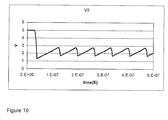
- 210 is off and V 2 equals to VDD as shown in FIG. 10
- inverter 212 's output V 3 is logic low as shown in FIG. 11
- Inverter 213 's output V 4 is logic high as shown in FIG. 12
- inverter 214 's output V 5 is logic low as shown in FIG. 13 , which keeps NMOS 204 off.
- I 1 starts charging capacitor 203
- voltage V 1 will rise linearly as shown in FIG. 9 because I 1 is a constant bias current to the first order.
- NMOS 210 is turned on and V 2 voltage starts decreasing as shown in FIG. 10 .
- V 2 Decreased V 2 changes inverter 212 's output V 3 to logic high, inverter 213 's output V 4 to logic low as shown in FIG. 12 , and inverter 214 's output to logic high.
- Inverter 214 's logic high output will turn on NMOS 204 and therefore discharge capacitor 203 .
- the voltage V 1 becomes low, which turns off NMOS 210 again and voltage V 2 become equal to VDD.
- This change also makes the output of NMOS 214 become logic zero and turns off NMOS 204 .
- I 1 starts charging capacitor 203 again. This process keeps repeating.
- the final oscillator clock can be taken from inverter 214 's output V 5 , or from register 215 's output ‘clock’ signal.
- V 2 has a very slow rising and falling slope as shown in FIG. 10 , which make inverter 212 spend more than necessary time in amplification mode, that means inverter 212 consume extra power, which is undesirable.
- V 3 signal has a very slow falling slope, making inverter 213 consume a lot power.
- V 5 has a square waveform according to FIG. 13 , and NMOS 204 is on when V 5 gives logic high. That means the bias current I 1 is directly injected into ground when V 5 is logic high, a waste of power.
- NMOS 210 should behave as close to a switch as possible, turned on and off. Also signal V 5 should have as low duty cycle as possible for low power consumption.
- FIG. 15 is an oscillator circuit in accordance with the present invention that includes a power saving feature.
- the circuit in FIG. 15 is the same as that in FIG. 8 except that there is one extra PMOS 216 introduced in FIG. 15 .
- PMOS 216 's gate is connected to the output of inverter 213 , its source is connected VDD and the drain is connected to the drain of PMOS 209 .
- NMOS 210 through inverter 212 , 213 and PMOS 216 form a close loop.
- NMOS 210 When NMOS 210 starts turning on, the drain voltage of NMOS 210 is still close to VDD and NMOS 210 is in active region. However, when NMOS 210 starts turning on, V 2 and V 4 start decreasing, which makes PMOS 216 try to hold voltage at V 2 close to logic high for more time than if there is no PMOS 216 and gate inverter 212 sees logic high input instead of an analog input.
- PMOS 216 injects extra current into NMOS 210 .
- PMOS 216 reduces NMOS 210 's turning on time with lower I bias current when compared with design having no PMOS 216 .
- Reduced turning-on time for NMOS 210 also finally reduces duty cycle for signal V 5 .
- PMOS 216 has two functions here: the first function is to achieve an oscillator with higher frequency at lower power consumption; the second function is to make NMOS 210 behave more like a switch. PMOS 216 only consume small dynamic transient current.
- FIG. 16 to FIG. 21 show waveforms of V 1 , V 2 , V 3 , V 4 , V 5 and output clock signal generated by circuit in FIG. 15 . It is clear that V 2 in FIG. 17 is more like a square waveform than that in FIG. 10 , which verifies that PMOS 216 makes NMOS 210 behave more like a switch.
- the size of NMOS 204 is large enough to make the discharging time constant negligible when compared with capacitor 203 's charging time.
- FIG. 22 shows one alternative way of implementation.
- there is no resistor 211 and the source of 210 is directly connected to ground.
- the drain of 208 and 210 are connected together. Therefore the compensation current is directly injected into the drain of 210 .
- FIG. 23 shows the optimum implementation of current invention.
- the device 204 and 210 are both implemented by NMOS transistors. They can also be implemented by N-type Junction-Gate-Field-Effect-Transistors (JFET), P-type JFET, or PMOS transistors.
- FIG. 24 shows the PMOS implementation of both device 204 and 210 .
- the source of PMOS 204 is connected to VDD and its drain is connected to the bottom plate of capacitor 203 .
- One end of resistor 211 is connected to VDD and the other end of this resistor is connected the source of PMOS 210 .
- the drain of PMOS 210 is connected to current source 14 .
- One end of the compensation current source 15 is connected to the source of PMOS 210 , while the other end of current source 15 is connected to ground.
- FIG. 25 shows the detailed implementation of FIG. 24 .
- the PMOS 201 in FIG. 15 is NMOS in FIG. 25 .
- the device 207 and 208 in FIG. 15 are removed in FIG. 25 .
- the compensation current is directly generated from the source of NMOS 205 .
- the summation node 404 in FIG. 15 is implemented by directly connecting I be and I ptat current together.
- the current in NMOS 201 and 221 are I bias current constant over the temperature to the first order.
- Besides 204 and 210 are PMOS, 216 are also PMOS.
- There is one more inverter 220 to keep the desired logic. When temperature increases, the threshold voltage of NMOS 205 is reduced.
- NMOS 205 over-driven voltage of NMOS 205 is increased, which results into an increased drain current in NMOS 205 .
- the current in 206 is constant. So, the increased current in NMOS 205 comes from resistor 211 as compensation current. Increased current in resistor 211 increases the source-bulk voltage of V SB for PMOS 210 to stabilize the threshold voltage of PMOS 210 .
Landscapes
- Engineering & Computer Science (AREA)
- Power Engineering (AREA)
- Logic Circuits (AREA)
- Inductance-Capacitance Distribution Constants And Capacitance-Resistance Oscillators (AREA)
Abstract
Description
V TH =V TH0+γ(√{square root over (|2ΦF +V SB|)}−√{square root over (|2ΦF|)}) (1)
V SB =I comp *R (2)
Where un is electron's mobility, COX is gate oxide capacitance, W and L are MOSFET's width and length respectively. VGS is the voltage between MOSFET's gate and source terminals, which is equal to Vbg or part of Vbg.
Claims (7)
Priority Applications (4)
| Application Number | Priority Date | Filing Date | Title |
|---|---|---|---|
| US12/553,931 US8044740B2 (en) | 2009-09-03 | 2009-09-03 | Temperature compensated RC oscillator for signal conditioning ASIC using source bulk voltage of MOSFET |
| JP2012528064A JP2013504263A (en) | 2009-09-03 | 2010-09-02 | Temperature compensated RC oscillator for signal processing ASIC using MOSFET source bulk voltage |
| PCT/US2010/047735 WO2011028946A1 (en) | 2009-09-03 | 2010-09-02 | A temperature compensated rc oscillator for signal conditioning asic using source bulk voltage of mosfet |
| EP10814523.6A EP2473891A4 (en) | 2009-09-03 | 2010-09-02 | A temperature compensated rc oscillator for signal conditioning asic using source bulk voltage of mosfet |
Applications Claiming Priority (1)
| Application Number | Priority Date | Filing Date | Title |
|---|---|---|---|
| US12/553,931 US8044740B2 (en) | 2009-09-03 | 2009-09-03 | Temperature compensated RC oscillator for signal conditioning ASIC using source bulk voltage of MOSFET |
Publications (2)
| Publication Number | Publication Date |
|---|---|
| US20110050353A1 US20110050353A1 (en) | 2011-03-03 |
| US8044740B2 true US8044740B2 (en) | 2011-10-25 |
Family
ID=43623960
Family Applications (1)
| Application Number | Title | Priority Date | Filing Date |
|---|---|---|---|
| US12/553,931 Expired - Fee Related US8044740B2 (en) | 2009-09-03 | 2009-09-03 | Temperature compensated RC oscillator for signal conditioning ASIC using source bulk voltage of MOSFET |
Country Status (4)
| Country | Link |
|---|---|
| US (1) | US8044740B2 (en) |
| EP (1) | EP2473891A4 (en) |
| JP (1) | JP2013504263A (en) |
| WO (1) | WO2011028946A1 (en) |
Cited By (3)
| Publication number | Priority date | Publication date | Assignee | Title |
|---|---|---|---|---|
| US9385649B2 (en) | 2014-05-29 | 2016-07-05 | Qualcomm Incorporated | RC oscillator based on delay-free comparator |
| US9473149B1 (en) | 2016-01-08 | 2016-10-18 | Qualcomm Incorporated | Temperature-compensated signal generator for supply voltage monitoring |
| US20230275545A1 (en) * | 2022-02-28 | 2023-08-31 | Texas Instruments Incorporated | Oscillator with reduced temperature sensitivity |
Families Citing this family (12)
| Publication number | Priority date | Publication date | Assignee | Title |
|---|---|---|---|---|
| JP6234008B2 (en) * | 2012-03-28 | 2017-11-22 | セイコーエプソン株式会社 | Oscillation circuit and electronic equipment |
| US9300302B2 (en) | 2012-04-20 | 2016-03-29 | Freescale Semiconductor, Inc. | Oscillator circuit, a semiconductor device and an apparatus |
| JP5974627B2 (en) * | 2012-05-21 | 2016-08-23 | セイコーエプソン株式会社 | Oscillation circuit and electronic equipment |
| US9484935B2 (en) | 2013-12-19 | 2016-11-01 | Analog Devices Global | Apparatus and methods for frequency lock enhancement of phase-locked loops |
| US9413366B2 (en) * | 2013-12-19 | 2016-08-09 | Analog Devices Global | Apparatus and methods for phase-locked loops with temperature compensated calibration voltage |
| CN105515550B (en) * | 2016-01-22 | 2017-12-29 | 英麦科(厦门)微电子科技有限公司 | A kind of super low-power consumption clock circuit with high stability |
| US10491155B2 (en) * | 2016-03-15 | 2019-11-26 | Texas Instruments Incorporated | Temperature compensated oscillator driver |
| FR3068189A1 (en) * | 2017-06-21 | 2018-12-28 | Stmicroelectronics (Rousset) Sas | RC OSCILLATOR |
| CN111404484B (en) * | 2020-04-26 | 2020-12-08 | 珠海迈巨微电子有限责任公司 | RC oscillators and electrical equipment |
| CN111769832B (en) * | 2020-06-28 | 2024-04-16 | 天津大学 | Self-adaptive ring oscillator |
| CN113381695B (en) * | 2021-05-07 | 2023-03-21 | 宁波市芯能微电子科技有限公司 | Clock oscillator circuit |
| CN113884209B (en) * | 2021-09-09 | 2023-10-10 | 芯原微电子(成都)有限公司 | Low-power consumption over-temperature detection circuit |
Citations (9)
| Publication number | Priority date | Publication date | Assignee | Title |
|---|---|---|---|---|
| JPS55115717A (en) * | 1979-03-01 | 1980-09-05 | Citizen Watch Co Ltd | Ring oscillator |
| US5870345A (en) | 1997-09-04 | 1999-02-09 | Siemens Aktiengesellschaft | Temperature independent oscillator |
| US6091286A (en) | 1994-02-14 | 2000-07-18 | Philips Electronics North America Corporation | Fully integrated reference circuit having controlled temperature dependence |
| US6377130B1 (en) | 2000-09-12 | 2002-04-23 | Rockwell Collins, Inc. | Temperature stabilized CMOS oscillator circuit |
| US20050134393A1 (en) | 2003-12-19 | 2005-06-23 | Kim Jung P. | Oscillator with temperature control |
| US20070233912A1 (en) | 2006-03-31 | 2007-10-04 | Silicon Laboratories Inc. | Precision oscillator having linbus capabilities |
| US20070241833A1 (en) | 2006-03-31 | 2007-10-18 | Silicon Laboratories Inc. | Precision oscillator having improved temperature coefficient control |
| US20090002084A1 (en) * | 2004-07-28 | 2009-01-01 | Akira Inoue | Oscillator |
| US20090153214A1 (en) | 2007-11-29 | 2009-06-18 | Nec Lcd Technologies, Ltd. | Delay element, variable delay line, and voltage controlled oscillator, as well as display device and system comprising the same |
Family Cites Families (2)
| Publication number | Priority date | Publication date | Assignee | Title |
|---|---|---|---|---|
| US6157270A (en) * | 1998-12-28 | 2000-12-05 | Exar Corporation | Programmable highly temperature and supply independent oscillator |
| DE10157292A1 (en) * | 2001-11-22 | 2003-06-05 | Infineon Technologies Ag | Temperature stabilized oscillator circuit |
-
2009
- 2009-09-03 US US12/553,931 patent/US8044740B2/en not_active Expired - Fee Related
-
2010
- 2010-09-02 JP JP2012528064A patent/JP2013504263A/en active Pending
- 2010-09-02 WO PCT/US2010/047735 patent/WO2011028946A1/en not_active Ceased
- 2010-09-02 EP EP10814523.6A patent/EP2473891A4/en not_active Withdrawn
Patent Citations (9)
| Publication number | Priority date | Publication date | Assignee | Title |
|---|---|---|---|---|
| JPS55115717A (en) * | 1979-03-01 | 1980-09-05 | Citizen Watch Co Ltd | Ring oscillator |
| US6091286A (en) | 1994-02-14 | 2000-07-18 | Philips Electronics North America Corporation | Fully integrated reference circuit having controlled temperature dependence |
| US5870345A (en) | 1997-09-04 | 1999-02-09 | Siemens Aktiengesellschaft | Temperature independent oscillator |
| US6377130B1 (en) | 2000-09-12 | 2002-04-23 | Rockwell Collins, Inc. | Temperature stabilized CMOS oscillator circuit |
| US20050134393A1 (en) | 2003-12-19 | 2005-06-23 | Kim Jung P. | Oscillator with temperature control |
| US20090002084A1 (en) * | 2004-07-28 | 2009-01-01 | Akira Inoue | Oscillator |
| US20070233912A1 (en) | 2006-03-31 | 2007-10-04 | Silicon Laboratories Inc. | Precision oscillator having linbus capabilities |
| US20070241833A1 (en) | 2006-03-31 | 2007-10-18 | Silicon Laboratories Inc. | Precision oscillator having improved temperature coefficient control |
| US20090153214A1 (en) | 2007-11-29 | 2009-06-18 | Nec Lcd Technologies, Ltd. | Delay element, variable delay line, and voltage controlled oscillator, as well as display device and system comprising the same |
Cited By (5)
| Publication number | Priority date | Publication date | Assignee | Title |
|---|---|---|---|---|
| US9385649B2 (en) | 2014-05-29 | 2016-07-05 | Qualcomm Incorporated | RC oscillator based on delay-free comparator |
| US9473149B1 (en) | 2016-01-08 | 2016-10-18 | Qualcomm Incorporated | Temperature-compensated signal generator for supply voltage monitoring |
| WO2017120244A1 (en) * | 2016-01-08 | 2017-07-13 | Qualcomm Incorporated | Temperature-compensated signal generator for supply voltage monitoring |
| US20230275545A1 (en) * | 2022-02-28 | 2023-08-31 | Texas Instruments Incorporated | Oscillator with reduced temperature sensitivity |
| US11799422B2 (en) * | 2022-02-28 | 2023-10-24 | Texas Instruments Incorporated | Oscillator with reduced temperature sensitivity |
Also Published As
| Publication number | Publication date |
|---|---|
| EP2473891A4 (en) | 2014-12-31 |
| JP2013504263A (en) | 2013-02-04 |
| WO2011028946A1 (en) | 2011-03-10 |
| US20110050353A1 (en) | 2011-03-03 |
| EP2473891A1 (en) | 2012-07-11 |
Similar Documents
| Publication | Publication Date | Title |
|---|---|---|
| US8044740B2 (en) | Temperature compensated RC oscillator for signal conditioning ASIC using source bulk voltage of MOSFET | |
| US8115559B2 (en) | Oscillator for providing a constant oscillation signal, and a signal processing device including the oscillator | |
| US8203392B2 (en) | Oscillator stabilized for temperature and power supply variations | |
| US7733191B2 (en) | Oscillator devices and methods thereof | |
| US7940135B2 (en) | Oscillation circuit | |
| US10747250B2 (en) | Integrated circuit with adaptability to a process-voltage-temperature (PVT) variation | |
| JP2007300623A (en) | Oscillation circuit with embedded power supply circuit | |
| Olmos | A temperature compensated fully trimmable on-chip IC oscillator | |
| US4383224A (en) | NMOS Crystal oscillator | |
| KR100753666B1 (en) | Ultra Low Power RC Oscillators | |
| US20060197610A1 (en) | Voltage controlled oscillator | |
| CN110601658B (en) | Automatic compensation of control voltage range of low voltage VCO | |
| CN110932670B (en) | Oscillator circuit and related oscillator device | |
| US6911869B2 (en) | Voltage controlled oscillator capable of linear operation at very low frequencies | |
| KR100520269B1 (en) | Voltage-current converter and self-oscillator using the same | |
| US6515537B2 (en) | Integrated circuit current source with switched capacitor feedback | |
| US11881817B2 (en) | Low power oscillator with variable duty cycle and method therefor | |
| US7321270B2 (en) | Current-controlled CMOS ring oscillator circuit | |
| KR19990076264A (en) | Charge-Discharge Oscillator Using Constant Current and Its Oscillation Method | |
| US7446597B2 (en) | Voltage-controlled current source and frequency scanner using the same | |
| US20250105826A1 (en) | Voltage mode relaxation oscillator | |
| US6154016A (en) | Voltage-to-current converting circuit which has a wide control range and which utilizes a depletion type field effect transistor | |
| JP3852924B2 (en) | Oscillator circuit | |
| US10658011B2 (en) | Voltage generating system, voltage generating circuit and associated method | |
| KR100557602B1 (en) | Temperature compensated oscillator |
Legal Events
| Date | Code | Title | Description |
|---|---|---|---|
| AS | Assignment |
Owner name: S3C, INC., CALIFORNIA Free format text: ASSIGNMENT OF ASSIGNORS INTEREST;ASSIGNOR:ZHU, ZHINENG;REEL/FRAME:023192/0778 Effective date: 20090831 |
|
| ZAAA | Notice of allowance and fees due |
Free format text: ORIGINAL CODE: NOA |
|
| ZAAB | Notice of allowance mailed |
Free format text: ORIGINAL CODE: MN/=. |
|
| STCF | Information on status: patent grant |
Free format text: PATENTED CASE |
|
| FPAY | Fee payment |
Year of fee payment: 4 |
|
| AS | Assignment |
Owner name: NAGANO KEIKI CO., LTD. (NKS), JAPAN Free format text: ASSIGNMENT OF ASSIGNORS INTEREST;ASSIGNOR:S3C INC. (S3C);REEL/FRAME:041837/0583 Effective date: 20170303 |
|
| FEPP | Fee payment procedure |
Free format text: ENTITY STATUS SET TO UNDISCOUNTED (ORIGINAL EVENT CODE: BIG.) |
|
| MAFP | Maintenance fee payment |
Free format text: PAYMENT OF MAINTENANCE FEE, 8TH YEAR, LARGE ENTITY (ORIGINAL EVENT CODE: M1552); ENTITY STATUS OF PATENT OWNER: LARGE ENTITY Year of fee payment: 8 |
|
| FEPP | Fee payment procedure |
Free format text: MAINTENANCE FEE REMINDER MAILED (ORIGINAL EVENT CODE: REM.); ENTITY STATUS OF PATENT OWNER: LARGE ENTITY |
|
| LAPS | Lapse for failure to pay maintenance fees |
Free format text: PATENT EXPIRED FOR FAILURE TO PAY MAINTENANCE FEES (ORIGINAL EVENT CODE: EXP.); ENTITY STATUS OF PATENT OWNER: LARGE ENTITY |
|
| STCH | Information on status: patent discontinuation |
Free format text: PATENT EXPIRED DUE TO NONPAYMENT OF MAINTENANCE FEES UNDER 37 CFR 1.362 |
|
| FP | Lapsed due to failure to pay maintenance fee |
Effective date: 20231025 |