US8044651B2 - Efficient PWM controller - Google Patents
Efficient PWM controller Download PDFInfo
- Publication number
- US8044651B2 US8044651B2 US12/331,529 US33152908A US8044651B2 US 8044651 B2 US8044651 B2 US 8044651B2 US 33152908 A US33152908 A US 33152908A US 8044651 B2 US8044651 B2 US 8044651B2
- Authority
- US
- United States
- Prior art keywords
- ramp
- current
- signal
- period
- saw
- Prior art date
- Legal status (The legal status is an assumption and is not a legal conclusion. Google has not performed a legal analysis and makes no representation as to the accuracy of the status listed.)
- Active, expires
Links
- 239000003990 capacitor Substances 0.000 claims abstract description 15
- 230000010354 integration Effects 0.000 claims abstract description 3
- 239000002131 composite material Substances 0.000 claims abstract 4
- 238000006243 chemical reaction Methods 0.000 description 10
- 238000010586 diagram Methods 0.000 description 9
- 238000012885 constant function Methods 0.000 description 2
- 238000013461 design Methods 0.000 description 2
- 238000000034 method Methods 0.000 description 2
- 238000012986 modification Methods 0.000 description 2
- 230000004048 modification Effects 0.000 description 2
- 230000000295 complement effect Effects 0.000 description 1
- 230000007274 generation of a signal involved in cell-cell signaling Effects 0.000 description 1
- 230000000737 periodic effect Effects 0.000 description 1
- 238000012552 review Methods 0.000 description 1
- 229920006395 saturated elastomer Polymers 0.000 description 1
- 238000012546 transfer Methods 0.000 description 1
- 230000009466 transformation Effects 0.000 description 1
- 239000002699 waste material Substances 0.000 description 1
Images


Classifications
-
- H—ELECTRICITY
- H02—GENERATION; CONVERSION OR DISTRIBUTION OF ELECTRIC POWER
- H02M—APPARATUS FOR CONVERSION BETWEEN AC AND AC, BETWEEN AC AND DC, OR BETWEEN DC AND DC, AND FOR USE WITH MAINS OR SIMILAR POWER SUPPLY SYSTEMS; CONVERSION OF DC OR AC INPUT POWER INTO SURGE OUTPUT POWER; CONTROL OR REGULATION THEREOF
- H02M3/00—Conversion of dc power input into dc power output
- H02M3/22—Conversion of dc power input into dc power output with intermediate conversion into ac
- H02M3/24—Conversion of dc power input into dc power output with intermediate conversion into ac by static converters
- H02M3/28—Conversion of dc power input into dc power output with intermediate conversion into ac by static converters using discharge tubes with control electrode or semiconductor devices with control electrode to produce the intermediate ac
- H02M3/325—Conversion of dc power input into dc power output with intermediate conversion into ac by static converters using discharge tubes with control electrode or semiconductor devices with control electrode to produce the intermediate ac using devices of a triode or a transistor type requiring continuous application of a control signal
- H02M3/335—Conversion of dc power input into dc power output with intermediate conversion into ac by static converters using discharge tubes with control electrode or semiconductor devices with control electrode to produce the intermediate ac using devices of a triode or a transistor type requiring continuous application of a control signal using semiconductor devices only
- H02M3/33507—Conversion of dc power input into dc power output with intermediate conversion into ac by static converters using discharge tubes with control electrode or semiconductor devices with control electrode to produce the intermediate ac using devices of a triode or a transistor type requiring continuous application of a control signal using semiconductor devices only with automatic control of the output voltage or current, e.g. flyback converters
-
- H—ELECTRICITY
- H03—ELECTRONIC CIRCUITRY
- H03K—PULSE TECHNIQUE
- H03K7/00—Modulating pulses with a continuously-variable modulating signal
- H03K7/08—Duration or width modulation ; Duty cycle modulation
-
- H—ELECTRICITY
- H02—GENERATION; CONVERSION OR DISTRIBUTION OF ELECTRIC POWER
- H02M—APPARATUS FOR CONVERSION BETWEEN AC AND AC, BETWEEN AC AND DC, OR BETWEEN DC AND DC, AND FOR USE WITH MAINS OR SIMILAR POWER SUPPLY SYSTEMS; CONVERSION OF DC OR AC INPUT POWER INTO SURGE OUTPUT POWER; CONTROL OR REGULATION THEREOF
- H02M1/00—Details of apparatus for conversion
- H02M1/0003—Details of control, feedback or regulation circuits
- H02M1/0032—Control circuits allowing low power mode operation, e.g. in standby mode
-
- Y—GENERAL TAGGING OF NEW TECHNOLOGICAL DEVELOPMENTS; GENERAL TAGGING OF CROSS-SECTIONAL TECHNOLOGIES SPANNING OVER SEVERAL SECTIONS OF THE IPC; TECHNICAL SUBJECTS COVERED BY FORMER USPC CROSS-REFERENCE ART COLLECTIONS [XRACs] AND DIGESTS
- Y02—TECHNOLOGIES OR APPLICATIONS FOR MITIGATION OR ADAPTATION AGAINST CLIMATE CHANGE
- Y02B—CLIMATE CHANGE MITIGATION TECHNOLOGIES RELATED TO BUILDINGS, e.g. HOUSING, HOUSE APPLIANCES OR RELATED END-USER APPLICATIONS
- Y02B70/00—Technologies for an efficient end-user side electric power management and consumption
- Y02B70/10—Technologies improving the efficiency by using switched-mode power supplies [SMPS], i.e. efficient power electronics conversion e.g. power factor correction or reduction of losses in power supplies or efficient standby modes
Definitions
- the present invention relates to a PWM (Pulse Width Modulation) controller, and more particularly to a PWM controller capable of performing power management in power conversion applications.
- PWM Pulse Width Modulation
- FIG. 1 shows the architecture of a typical application of PWM controller.
- the architecture realizing a fly-back type power converter at least includes: a PWM controller 100 , an input rectifier and filter 101 , a main transformer 102 , an output rectifier and filter 103 , a feedback network 104 , and an NMOS transistor 105 .
- the PWM controller 100 is used for generating a pulse signal S P in response to a feedback signal V FB .
- the input rectifier and filter 101 is used for generating a first DC voltage according to an AC input power source.
- the main transformer 102 and the output rectifier and filter 103 are used to transfer the first DC voltage to a DC output voltage V O .
- the feedback network 104 is used to generate the feedback signal V FB according to the DC output voltage V O .
- the NMOS transistor 105 is used to control the power transformation through the main transformer 102 in response to the pulse signal S P .
- FIG. 2 shows the circuit diagram of a prior art PWM controller.
- the prior art PWM controller at least includes: a saw-tooth signal generator 200 , a trigger generator 201 , a latch 202 , a NOT gate 203 , a NOT gate 204 , a reset generator 205 and an output stage 206 .
- the saw-tooth signal generator 200 is used for generating a saw-tooth signal V SAW in response to an ICKB signal and an ICK signal, and comprises a current source I UP , a switch SW UP , a capacitor C T , a switch SW DN and a current source I DN .
- the switch SW UP When the switch SW UP is on, the current source I UP flowing into the capacitor C T will cause the saw-tooth signal V SAW to ramp up; when the switch SW DN is on, the current source I DN flowing out from the capacitor C T will cause the saw-tooth signal V SAW to ramp down.
- the trigger generator 201 is used to generate a pair of trigger signals for the latch 202 according to the comparisons of the saw-tooth signal V SAW to a level V H and a level V L .
- the latch 202 is used for generating a CKB signal and a CK signal according to the pair of trigger signals, in which the CKB signal is a complement to the CK signal.
- the NOT gate 203 is used to generate the ICKB signal according to the CKB signal; the NOT gate 204 is used to generate the ICK signal according to the CK signal.
- the reset generator 205 is used for generating a RESET signal according to a ramp signal V S and a V + signal which is derived from the feedback signal V FB .
- the pulse signal S P of the output stage 206 will be pulled down to low logic level and the NMOS transistor 105 (shown in FIG. 1 ) will therefore be turned off.
- the output stage 206 is used to generate the pulse signal S P in response to the CK signal and the RESET signal.
- the timing relation among the saw-tooth signal V SAW , CKB signal, V + signal, ramp signal V S and pulse signal S P is shown in FIG. 3 .
- the ramp-up period and the ramp down period are fixed, so the period of the pulse signal S P is fixed.
- the NMOS transistor 105 shown in FIG. 1 ) will be switched at a fixed frequency regardless the loading condition of the fly-back type power converter. However, if the loading condition is in light load or in empty load, this design will waste much power and surely does not comply with the energy-saving requirement.
- an objective of the present invention is to provide a PWM controller having an efficient way of power management that can reduce the power consumption of a power conversion application when the loading is in light load or empty load.
- a still another objective of the present invention is to further provide an efficient PWM controller capable of operating in a first mode or a second mode according to a mode selecting signal.
- a still another objective of the present invention is to further provide an efficient PWM controller comprising a saw-tooth signal generator for generating a first saw-tooth signal of the first mode or a second saw-tooth signal of the second mode, wherein the first saw-tooth signal comprises a first ramp-up period and a first ramp-down period, and the second saw-tooth signal comprises a second ramp-up period and a second ramp-down period.
- the present novel means of saw-tooth signal generation providing a first saw-tooth signal of the first mode or a second saw-tooth signal of the second mode, can be utilized in a PWM controller to reduce the power consumption of related power conversion applications when the loading is in light load or empty load.
- the power conversion applications can be AC/DC, DC/DC, AC/AC or DC/AC.
- the efficient PWM controller capable of operating in the first mode, for example but not limited to a normal mode, or in the second mode, for example but not limited to a green mode, comprises a saw-tooth signal generator for generating a first saw-tooth signal of the normal mode or a second saw-tooth signal of the green mode, in response to a mode selecting signal.
- the first saw-tooth signal includes a first ramp-up period and a first ramp-down period;
- the second saw-tooth signal includes a second ramp-up period and a second ramp-down period; the second ramp-up period is longer than the first ramp-up period, and the second ramp-down period is longer than the first ramp-down period.
- the first ramp-up period plus the first ramp-down period results in a first switching period
- the second ramp-up period plus the second ramp-down period results in a second switching period.
- the second switching period corresponding to the green mode is longer than the first switching period corresponding to the normal mode due to the design that the second ramp-up period is longer than the first ramp-up period, and the second ramp-down period is longer than the first ramp-down period.
- FIG. 1 is the architecture of a typical application of PWM controller.
- FIG. 2 is a circuit diagram of a prior art PWM controller.
- FIG. 3 is a wave-form diagram for major signals in a prior art PWM controller.
- FIG. 4 shows the wave-form of one ramp-up period plus one ramp-down period of saw-tooth signals in the normal mode as well as in the green mode for a preferred embodiment of the present invention.
- FIG. 5 is a block diagram of PWM controller of a preferred embodiment of the present invention.
- FIG. 6 is a circuit diagram of a saw-tooth generator operating in the green mode for the PWM controller of a preferred embodiment of the present invention.
- FIG. 7 is a block diagram of a pulse width limiter of a preferred embodiment of the present invention.
- the dynamic power consumption of the switching circuit due to the energy-storing elements will be increased as the switching frequency goes up.
- the switching frequency designed for the normal load is much higher than that needed for the light load or empty load.
- the prior art PWM controller with fixed switching period regardless the loading condition will consume a lot of unnecessary power when operating in light load or empty load.
- the present invention grasps this point and offers a solution which will be disclosed in the following description.
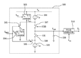
- FIG. 5 shows a block diagram of PWM controller of a preferred embodiment of the present invention.
- the PWM controller includes a saw-tooth signal generator 500 and a pulse generator 510 .
- the saw-tooth signal generator 500 is used for generating a corresponding saw-tooth signal V SAW in response to a mode selecting signal S MODE , and comprises: a constant current source 501 , a constant current source 502 , a voltage to current converter 503 , a voltage to current converter 504 , a switch 505 , a switch 506 , a switch 507 , a switch 508 and a capacitor 509 .
- the constant current source 501 is used to generate a constant current I UP .
- the constant current source 502 is used to generate a constant current I DN .
- the voltage to current converter 503 is used to generate a current I UPA in response to a feedback voltage V FB .
- the voltage to current converter 504 is used to generate a current I DNA in response to a feedback voltage V FB .
- the switch 505 is used to connect the constant current source 501 with the voltage to current converter 504 in response to the mode selecting signal S MODE .
- S MODE indicates the normal mode
- the switch 505 is off; when S MODE indicates the green mode, the switch 505 is on.
- the switch 506 is used to connect the constant current source 502 with the voltage to current converter 503 in response to the mode selecting signal S MODE .
- S MODE indicates the normal mode
- the switch 506 is off; when S MODE indicates the green mode, the switch 506 is on.
- the switch 507 is used to connect the constant current source 501 with the capacitor 509 in response to the ICKB signal.
- the switch 508 is used to connect the constant current source 502 with the capacitor 509 in response to the ICK signal.
- the capacitor 509 is used to build the saw-tooth signal V SAW by current integration.
- the pulse generator 510 is used to generate the pulse signal S P in response to the saw-tooth signal V SAW and the feedback voltage V FB .
- the voltage to current converter 503 generates the current I UPA according to a first function of the feedback voltage V FB
- the voltage to current converter 504 generates the current I DNA according to a second function of the feedback voltage V FB .
- the current I UPA is smaller than the current I DN and the current I DNA is smaller than the current I UP
- the first function and second function are preferably first order polynomials of the feedback voltage V FB .
- the saw-tooth signal generator includes: a PMOS transistor 601 , an NMOS transistor 602 , a PMOS transistor 603 , an NMOS transistor 604 , an NMOS transistor 605 , an OPA 606 , a resistor 607 , a PMOS transistor 608 , an NMOS transistor 609 , a PMOS transistor 610 , an NMOS transistor 611 , a switch 612 , a switch 613 and a capacitor 614 .
- the PMOS transistor 601 is used to duplicate the current I to other branches.
- the PMOS transistor 603 is used to mirror the current I from the PMOS transistor 601 .
- the NMOS transistor 605 is used to provide the current path for current I.
- the OPA 606 is used as a unit-gain buffer.
- the PMOS transistor 608 is used to mirror the current I from the PMOS transistor 601 .
- the NMOS transistor 609 is used to duplicate the current I to other branches.
- the PMOS transistor 610 is used to generate the current I UPA according to the current I.
- the NMOS transistor 611 is used to generate the current I DNA according to the current I.
- switch 612 The roles of switch 612 , switch 613 and capacitor 614 are the same with those of the switch 507 , switch 508 and capacitor 509 described in FIG. 5 .
- both the first function and second function can still be of other forms, for example but not limited to constant function.
- constant function the green mode switching period which is longer than the normal mode switching period is kept constant.
- FIG. 7 shows a block diagram of a pulse width limiter 700 .
- the pulse width limiter 700 includes a one-shot pulse generator 701 and an AND gate 702 .
- the one-shot pulse generator 701 is used to generate a single pulse S PL of a fixed pulse width in response to the pulse signal S P .
- the AND gate 702 is used to generate an output signal S OUT in response to the single pulse S PL and the pulse signal S P .
- the present invention herein enhances the performance than the conventional structure and further complies with the patent application requirements and is submitted to the Patent and Trademark Office for review and granting of the commensurate patent rights.
Abstract
Description
Claims (8)
Priority Applications (1)
| Application Number | Priority Date | Filing Date | Title |
|---|---|---|---|
| US12/331,529 US8044651B2 (en) | 2008-12-10 | 2008-12-10 | Efficient PWM controller |
Applications Claiming Priority (1)
| Application Number | Priority Date | Filing Date | Title |
|---|---|---|---|
| US12/331,529 US8044651B2 (en) | 2008-12-10 | 2008-12-10 | Efficient PWM controller |
Publications (2)
| Publication Number | Publication Date |
|---|---|
| US20100141033A1 US20100141033A1 (en) | 2010-06-10 |
| US8044651B2 true US8044651B2 (en) | 2011-10-25 |
Family
ID=42230269
Family Applications (1)
| Application Number | Title | Priority Date | Filing Date |
|---|---|---|---|
| US12/331,529 Active 2030-05-21 US8044651B2 (en) | 2008-12-10 | 2008-12-10 | Efficient PWM controller |
Country Status (1)
| Country | Link |
|---|---|
| US (1) | US8044651B2 (en) |
Cited By (2)
| Publication number | Priority date | Publication date | Assignee | Title |
|---|---|---|---|---|
| US20110228579A1 (en) * | 2010-03-16 | 2011-09-22 | Chin-Yen Lin | Adjustable Frequency Generator and Related Power Supply |
| CN106105034A (en) * | 2014-04-16 | 2016-11-09 | 密克罗奇普技术公司 | Slope generation module |
Citations (5)
| Publication number | Priority date | Publication date | Assignee | Title |
|---|---|---|---|---|
| US5760623A (en) * | 1995-10-13 | 1998-06-02 | Texas Instruments Incorporated | Ramp voltage generator for differential switching amplifiers |
| US6519165B2 (en) * | 2000-12-04 | 2003-02-11 | Sanken Electric Co., Ltd. | Dc-to-dc converter |
| US7106130B2 (en) * | 2003-09-05 | 2006-09-12 | Delta Electronics, Inc. | Variable frequency PWM controller circuit |
| US7800352B2 (en) * | 2007-05-16 | 2010-09-21 | Intersil Americas Inc. | Controller having comp node voltage shift cancellation for improved discontinuous conduction mode (DCM) regulator performance and related methods |
| US7928715B2 (en) * | 2008-04-22 | 2011-04-19 | Seiko Instruments Inc. | Switching regulator |
-
2008
- 2008-12-10 US US12/331,529 patent/US8044651B2/en active Active
Patent Citations (5)
| Publication number | Priority date | Publication date | Assignee | Title |
|---|---|---|---|---|
| US5760623A (en) * | 1995-10-13 | 1998-06-02 | Texas Instruments Incorporated | Ramp voltage generator for differential switching amplifiers |
| US6519165B2 (en) * | 2000-12-04 | 2003-02-11 | Sanken Electric Co., Ltd. | Dc-to-dc converter |
| US7106130B2 (en) * | 2003-09-05 | 2006-09-12 | Delta Electronics, Inc. | Variable frequency PWM controller circuit |
| US7800352B2 (en) * | 2007-05-16 | 2010-09-21 | Intersil Americas Inc. | Controller having comp node voltage shift cancellation for improved discontinuous conduction mode (DCM) regulator performance and related methods |
| US7928715B2 (en) * | 2008-04-22 | 2011-04-19 | Seiko Instruments Inc. | Switching regulator |
Cited By (3)
| Publication number | Priority date | Publication date | Assignee | Title |
|---|---|---|---|---|
| US20110228579A1 (en) * | 2010-03-16 | 2011-09-22 | Chin-Yen Lin | Adjustable Frequency Generator and Related Power Supply |
| CN106105034A (en) * | 2014-04-16 | 2016-11-09 | 密克罗奇普技术公司 | Slope generation module |
| CN106105034B (en) * | 2014-04-16 | 2020-10-27 | 密克罗奇普技术公司 | Slope generation module |
Also Published As
| Publication number | Publication date |
|---|---|
| US20100141033A1 (en) | 2010-06-10 |
Similar Documents
| Publication | Publication Date | Title |
|---|---|---|
| Chen et al. | A SIMO parallel-string driver IC for dimmable LED backlighting with local bus voltage optimization and single time-shared regulation loop | |
| JP5664327B2 (en) | Control device for DC-DC converter | |
| JP4246045B2 (en) | Power supply circuit and method for raising output voltage of power supply circuit | |
| US7397151B2 (en) | Power supply unit and portable apparatus using the same | |
| US7095638B2 (en) | Controller for complementary switches of a power converter and method of operation thereof | |
| JP4631916B2 (en) | Boost DC-DC converter | |
| US20080259646A1 (en) | Dynamic converter topology | |
| JP5474988B2 (en) | Fast recovery control circuit | |
| JP2006050894A (en) | Power feeding for multiple load by dc-dc converter | |
| JP2008043195A (en) | Switching regulator and method for operating the same | |
| JP2010268646A (en) | Power supply controller, power supply, and power supply control method | |
| JP2007095907A (en) | Driving circuit and electronic apparatus using the same | |
| US20070115703A1 (en) | Soft-transition controller, method of controlling a soft transition and a synchronous converter employing the same | |
| JP2011060696A (en) | Pwm light dimming circuit | |
| JP2008245419A (en) | Load detecting circuit, and switching power circuit | |
| US8884545B2 (en) | LED driving system and driving method thereof | |
| JP2008017663A (en) | Switching power supply device | |
| US8044651B2 (en) | Efficient PWM controller | |
| JP5630895B2 (en) | Switching power supply circuit | |
| JP2007236051A (en) | Switching regulator | |
| JP2010063231A (en) | Switching regulator | |
| JP2008061371A (en) | Self-excited resonant switching power supply | |
| JP2006238603A (en) | Switching regulator | |
| JP2014112996A (en) | Light load detection circuit, switching regulator, and method of controlling the same | |
| KR102031009B1 (en) | Dc-dc buck converter |
Legal Events
| Date | Code | Title | Description |
|---|---|---|---|
| AS | Assignment |
Owner name: GRENERGY OPTO., INC.,TAIWAN Free format text: ASSIGNMENT OF ASSIGNORS INTEREST;ASSIGNORS:WANG, YEN-HUI;LIN, CHIN-YEN;HUNG, CHIA-CHIEH;AND OTHERS;REEL/FRAME:021951/0680 Effective date: 20081205 Owner name: GRENERGY OPTO., INC., TAIWAN Free format text: ASSIGNMENT OF ASSIGNORS INTEREST;ASSIGNORS:WANG, YEN-HUI;LIN, CHIN-YEN;HUNG, CHIA-CHIEH;AND OTHERS;REEL/FRAME:021951/0680 Effective date: 20081205 |
|
| STCF | Information on status: patent grant |
Free format text: PATENTED CASE |
|
| FPAY | Fee payment |
Year of fee payment: 4 |
|
| AS | Assignment |
Owner name: NANJING GREENCHIP SEMICONDUCTOR CO., LTD., CHINA Free format text: ASSIGNMENT OF ASSIGNORS INTEREST;ASSIGNOR:GRENERGY OPTO, INC.;REEL/FRAME:042702/0162 Effective date: 20170607 |
|
| MAFP | Maintenance fee payment |
Free format text: PAYMENT OF MAINTENANCE FEE, 8TH YR, SMALL ENTITY (ORIGINAL EVENT CODE: M2552); ENTITY STATUS OF PATENT OWNER: SMALL ENTITY Year of fee payment: 8 |
|
| MAFP | Maintenance fee payment |
Free format text: PAYMENT OF MAINTENANCE FEE, 12TH YR, SMALL ENTITY (ORIGINAL EVENT CODE: M2553); ENTITY STATUS OF PATENT OWNER: SMALL ENTITY Year of fee payment: 12 |