US8044405B2 - Thin film transistor substrate and manufacturing method thereof - Google Patents
Thin film transistor substrate and manufacturing method thereof Download PDFInfo
- Publication number
- US8044405B2 US8044405B2 US12/429,388 US42938809A US8044405B2 US 8044405 B2 US8044405 B2 US 8044405B2 US 42938809 A US42938809 A US 42938809A US 8044405 B2 US8044405 B2 US 8044405B2
- Authority
- US
- United States
- Prior art keywords
- passivation layer
- gate
- data
- layer
- pad
- Prior art date
- Legal status (The legal status is an assumption and is not a legal conclusion. Google has not performed a legal analysis and makes no representation as to the accuracy of the status listed.)
- Active, expires
Links
Images


Classifications
-
- H—ELECTRICITY
- H10—SEMICONDUCTOR DEVICES; ELECTRIC SOLID-STATE DEVICES NOT OTHERWISE PROVIDED FOR
- H10D—INORGANIC ELECTRIC SEMICONDUCTOR DEVICES
- H10D86/00—Integrated devices formed in or on insulating or conducting substrates, e.g. formed in silicon-on-insulator [SOI] substrates or on stainless steel or glass substrates
-
- G—PHYSICS
- G02—OPTICS
- G02F—OPTICAL DEVICES OR ARRANGEMENTS FOR THE CONTROL OF LIGHT BY MODIFICATION OF THE OPTICAL PROPERTIES OF THE MEDIA OF THE ELEMENTS INVOLVED THEREIN; NON-LINEAR OPTICS; FREQUENCY-CHANGING OF LIGHT; OPTICAL LOGIC ELEMENTS; OPTICAL ANALOGUE/DIGITAL CONVERTERS
- G02F1/00—Devices or arrangements for the control of the intensity, colour, phase, polarisation or direction of light arriving from an independent light source, e.g. switching, gating or modulating; Non-linear optics
- G02F1/01—Devices or arrangements for the control of the intensity, colour, phase, polarisation or direction of light arriving from an independent light source, e.g. switching, gating or modulating; Non-linear optics for the control of the intensity, phase, polarisation or colour
- G02F1/13—Devices or arrangements for the control of the intensity, colour, phase, polarisation or direction of light arriving from an independent light source, e.g. switching, gating or modulating; Non-linear optics for the control of the intensity, phase, polarisation or colour based on liquid crystals, e.g. single liquid crystal display cells
- G02F1/133—Constructional arrangements; Operation of liquid crystal cells; Circuit arrangements
- G02F1/136—Liquid crystal cells structurally associated with a semi-conducting layer or substrate, e.g. cells forming part of an integrated circuit
- G02F1/1362—Active matrix addressed cells
- G02F1/136227—Through-hole connection of the pixel electrode to the active element through an insulation layer
-
- H—ELECTRICITY
- H10—SEMICONDUCTOR DEVICES; ELECTRIC SOLID-STATE DEVICES NOT OTHERWISE PROVIDED FOR
- H10D—INORGANIC ELECTRIC SEMICONDUCTOR DEVICES
- H10D86/00—Integrated devices formed in or on insulating or conducting substrates, e.g. formed in silicon-on-insulator [SOI] substrates or on stainless steel or glass substrates
- H10D86/01—Manufacture or treatment
- H10D86/021—Manufacture or treatment of multiple TFTs
- H10D86/0231—Manufacture or treatment of multiple TFTs using masks, e.g. half-tone masks
-
- H—ELECTRICITY
- H10—SEMICONDUCTOR DEVICES; ELECTRIC SOLID-STATE DEVICES NOT OTHERWISE PROVIDED FOR
- H10D—INORGANIC ELECTRIC SEMICONDUCTOR DEVICES
- H10D86/00—Integrated devices formed in or on insulating or conducting substrates, e.g. formed in silicon-on-insulator [SOI] substrates or on stainless steel or glass substrates
- H10D86/40—Integrated devices formed in or on insulating or conducting substrates, e.g. formed in silicon-on-insulator [SOI] substrates or on stainless steel or glass substrates characterised by multiple TFTs
- H10D86/451—Integrated devices formed in or on insulating or conducting substrates, e.g. formed in silicon-on-insulator [SOI] substrates or on stainless steel or glass substrates characterised by multiple TFTs characterised by the compositions or shapes of the interlayer dielectrics
-
- H—ELECTRICITY
- H10—SEMICONDUCTOR DEVICES; ELECTRIC SOLID-STATE DEVICES NOT OTHERWISE PROVIDED FOR
- H10D—INORGANIC ELECTRIC SEMICONDUCTOR DEVICES
- H10D86/00—Integrated devices formed in or on insulating or conducting substrates, e.g. formed in silicon-on-insulator [SOI] substrates or on stainless steel or glass substrates
- H10D86/40—Integrated devices formed in or on insulating or conducting substrates, e.g. formed in silicon-on-insulator [SOI] substrates or on stainless steel or glass substrates characterised by multiple TFTs
- H10D86/60—Integrated devices formed in or on insulating or conducting substrates, e.g. formed in silicon-on-insulator [SOI] substrates or on stainless steel or glass substrates characterised by multiple TFTs wherein the TFTs are in active matrices
Definitions
- the present invention relates to a thin film transistor (“TFT”) array substrate and a method of fabricating the same, and more particularly, to a TFT array substrate in which a driving margin may be increased and a sufficiently large contact area between conductive materials may be provided in a contact portion, and a method of fabricating the TFT array substrate.
- TFT thin film transistor
- a liquid crystal display includes two opposing display panels and a liquid crystal layer interposed therebetween.
- Each display panel may use a transparent insulating substrate as a supporting substrate.
- a plurality of thin film patterns may be formed on the insulating substrate.
- a thin film pattern formation includes a material deposition and a mask process.
- a photolithography process may include multiple steps, such as photoresist coating, mask arrangement, exposure, baking, development, and cleaning, thus increasing the entire processing time and the manufacturing cost.
- a lift-off method has been studied. More specifically, when a passivation film and a pixel electrode are formed on a TFT array substrate, the passivation film is patterned using a photoresist pattern, a conductive material is deposited on the entire surface of the TFT array substrate, and the photoresist pattern and the conductive material thereon are simultaneously removed using a photoresist stripper. The conductive material remaining on the substrate forms a pixel electrode.
- the photoresist stripper may contact the sides or bottom of the photoresist pattern to remove the photoresist pattern covered with the conductive material.
- the contact area of the photoresist pattern with the photoresist stripper should be sufficiently large.
- the passivation film under the photoresist pattern should form a sufficiently large undercut under the inner side of the photoresist pattern.
- an insulating film on a storage electrode may be over-etched and its thickness may become non-uniform, thus causing a reduction in a driving margin.
- a data interconnection line may be damaged by over-etching, and etching of the data interconnection line in a contact area may cause contact failure.
- This invention provides a TFT array substrate that increases a driving margin and provides a sufficiently large contact area between conductive materials in a contact portion.
- the present invention also provides a TFT array substrate that enables easy lift-off and prevents over-etching of a gate insulating layer and damage to a data interconnection line.
- the present invention discloses a thin film transistor (TFT) substrate including a gate interconnection line comprising a gate line and a gate electrode arranged on an insulating substrate, a gate insulating layer formed on the gate interconnection line, a semiconductor layer formed on the gate insulating layer, a data interconnection line comprising a data line, a source electrode, and a drain electrode formed on the semiconductor layer, a first passivation layer formed on the data interconnection line and exposing a portion of the drain electrode, a second passivation layer formed on the first passivation film, wherein the outer sidewalls of the second passivation film are positioned inside the outer sidewalls of the first passivation film and a pixel electrode connected to the drain electrode.
- TFT thin film transistor
- the present invention also discloses a method of fabricating a thin film transistor (TFT) substrate.
- the method includes forming a gate interconnection line on an insulating substrate, the gate interconnection line comprising a gate line and a gate electrode, forming a gate insulating layer on the gate interconnection line, forming a semiconductor layer and a data interconnection line on the semiconductor layer, the data interconnection line comprising a data line, a source electrode, and a drain electrode, sequentially forming a first passivation layer and a second passivation layer on the data interconnection line, the second passivation layer has more porous lattice structure than that of the first passivation layer, etching the second passivation layer and the first passivation layer, and exposing a drain electrode of a drain electrode-pixel electrode contact portion and forming a pixel electrode connected to the drain electrode, wherein etching the second passivation layer and the first passivation layer comprises forming the outer sidewalls of the second passivation layer inside the outer sidewall
- FIG. 1 is a layout of a TFT substrate according to an exemplary embodiment of the invention.
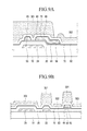
- FIG. 2A is a cross-sectional view taken along line A-A′ of FIG. 1 .
- FIG. 2B is a cross-sectional view taken along line B-B′ of FIG. 1 .
- FIG. 2C is a cross-sectional view taken along line C-C′ of FIG. 1 .
- FIGS. 3A , 4 A, 5 A, 6 A, 7 A, 8 A, 9 A, 10 A, 11 A and 12 A are cross-sectional views showing processing steps of the method of fabricating the TFT substrate shown in FIG. 2A according to an exemplary embodiment of the invention.
- FIGS. 3B , 4 B, 5 B, 6 B, 7 B, 8 B, 9 B, 10 B, 11 B and 12 B are cross-sectional views showing processing steps of the method of fabricating the TFT substrate shown in FIG. 2B according to an exemplary embodiment of the invention.
- FIGS. 3C , 4 C, 5 C, 6 C, 7 C, 8 C, 9 C, 10 C, 11 C and 12 C are cross-sectional views showing processing steps of the method of fabricating the TFT substrate in FIG. 2C according to an exemplary embodiment of the invention.
- FIGS. 13A to 14C are cross-sectional views showing processing steps of the method of fabricating the TFT substrate according to another exemplary embodiment of the invention
- FIG. 1 is a layout of a TFT substrate according to an exemplary embodiment of the invention
- FIG. 2A , FIG. 2B , and FIG. 2C are cross-sectional views taken along lines A-A′, B-B′, and C-C′, respectively, of FIG. 1 .
- a TFT substrate includes a TFT formed on an insulating substrate, a first passivation layer covering the TFT, and a second passivation layer formed on the first passivation layer.
- the TFT is a three-terminal device including a control terminal, an input terminal, and an output terminal and may include a gate electrode, a source electrode, a drain electrode, and a semiconductor layer.
- the gate electrode may be the control terminal
- the source electrode may be the input terminal
- the drain electrode may be the output terminal.
- the semiconductor layer may form a channel region of the TFT.
- an insulating substrate 10 supports a TFT and may be formed of, for example, transparent glass or plastic.
- a gate line 22 , a gate pad 27 and a gate electrode 24 are formed on the insulating substrate 10 .
- the gate line 22 for transmitting gate signal is disposed on the insulating substrate 10 .
- the gate lines 22 are spaced apart from each other and extend parallel with each other in a first direction, such as a row direction shown in FIG. 1 .
- a gate pad 27 having an expanded width is connected to an end of each gate line 22 .
- the gate pad 27 may be formed at two opposite terminals of the gate line 22 , or may be omitted.
- the gate electrode 24 is connected to the gate line 22 .
- Each gate electrode 24 may extend from the gate line 22 .
- the gate electrode 24 , the gate line 22 , and the gate pad 27 may be formed directly on the insulating substrate 10 .
- the gate electrode 24 , the gate line 22 , and the gate pad 27 are referred to as a gate interconnection line for the convenience of explanation.
- the storage electrode 28 which may be formed of the same material as the gate interconnection line, may be formed directly on the insulating substrate 10 .
- the storage electrode 28 is formed between the gate lines 22 and extends in the first direction parallel to the gate line 22 .
- a storage electrode pad (not shown), which may be similar to the gate pad 27 , may be made at one terminal of the storage electrode 28 .
- the shape of the storage electrode 28 may vary and the invention is not limited to the shape shown in FIG. 1 .
- the gate interconnection line and the storage electrode 28 may be formed as a single layer such as aluminum (Al), copper (Cu), silver (Ag), molybdenum (Mo), chrome (Cr), titanium (Ti), tantalum (Ta), or alloys thereof, or as a multi-layered structure including combinations of these materials, but the invention is not limited thereto.
- the gate insulation layer 30 may be formed of silicon nitride (SiNx) and may be formed on the gate interconnection line and the storage electrode 28 . However, the gate insulation layer 30 may not be formed on the gate interconnection line in a gate contact portion 76 where the gate pad 27 contacts an auxiliary gate pad 96 .
- a semiconductor layer 44 and ohmic contact layers 52 , 55 and 56 which may be formed of silicide or n+ hydrogenated amorphous silicon doped with n-type impurities, are formed on the gate insulating layer 30 .
- the semiconductor layer 44 has substantially the same pattern as data interconnection lines, which will be described in further detail below, except for the channel region.
- a channel region of a thin film transistor corresponds to where the semiconductor layer 44 overlaps with the gate electrode 24 .
- the data line 62 , the data pad 67 , the source electrode 65 , and the drain electrode 66 are formed on the semiconductor layer 44 and on the ohmic contact layers 52 , 55 and 56 .
- the data lines 62 are spaced apart from each other and extend parallel with each other in a second direction, such as a column direction shown in FIG. 1 .
- the data lines 62 cross with the gate lines 22 .
- a data pad 67 having an expanded width is connected to an end of each data line 62 .
- the data pad 67 may be formed at two opposite terminals of the data line 62 , or may be omitted.
- the source electrode 65 is connected to the data line 62 .
- Each source electrode 62 is opposite to and faces a drain electrode 66 .
- the semiconductor layer 44 may be exposed between the source electrode 65 and the drain electrode 66 .
- the data line 62 , the data pad 67 , the source electrode 62 , and the drain electrode 66 are referred to as a data interconnection line for the convenience of explanation.
- the data interconnection line may be formed as a single layer of Al, Cu, Ag, Mo, Cr, Ti, Ta, or alloys thereof, or as a multi-layered structure including combinations of these materials, but the invention is not limited thereto.
- a first passivation layer 70 is arranged on the data interconnection line except in an area where the drain electrode 66 contacts the pixel electrode 90 , referred to as a drain electrode-pixel electrode contact portion 101 , and except in an area where the data pad 67 contacts an auxiliary data pad 97 , referred to as a data contact portion 77 .
- the first passivation layer 70 is also formed on the channel region of the thin film transistor.
- the first passivation layer 70 is formed on the gate interconnection line except for the gate contact portion 76 . Specifically, in an area where the gate interconnection line does not overlap with the data interconnection line, the first passivation layer 70 is formed on the gate insulating layer 30 in a region corresponding to the gate interconnection line.
- the first passivation layer 70 is formed on the corresponding data interconnection line. In the space between the source electrode 65 and the drain electrode 66 , which overlaps with the gate electrode 24 , the first passivation layer 70 is formed on the semiconductor layer 44 .
- the first passivation layer 70 may be formed of silicon nitride (SiNx) which is the same material as the gate insulating layer 30 .
- the first passivation layer 70 is characterized that it has a dense lattice structure.
- the first passivation layer 70 may have a thickness in a range of about 50 ⁇ to about 500 ⁇ , or in a range of about 100 ⁇ to about 300 ⁇ .
- a second passivation layer 80 is formed on the first passivation layer 70 .
- the second passivation layer 80 may overlap with the first passivation layer 70 .
- the outer sidewall of the second passivation layer 80 is positioned inside the outer sidewall of the first passivation layer 70 . In other words, the sidewall of the first passivation layer 70 extends beyond the sidewall of the second passivation layer 80 .
- the second passivation layer 80 may be formed of silicon nitride (SiNx) which is the same material as the first passivation layer 70 . However the second passivation layer 80 has a porous lattice structure compared to the lattice structure of the first passivation layer 70 .
- the second passivation layer 80 may have a thickness in a range of about 1,000 ⁇ to about 3,000 ⁇ , or in a range of about 1,500 ⁇ to about 2,500 ⁇ .
- the first passivation layer 70 and the second passivation layer 80 may protect lower structures such as the data interconnection line, the semiconductor layer 44 , and the gate interconnection line.
- the gate contact portion 76 is formed through the gate insulating layer 30 , the first passivation layer 70 and the second passivation layer 80 .
- the data contact portion 77 is formed through the first passivation layer 70 and the second passivation layer 80 .
- the pixel electrode 90 may be made of a transparent conductive material such as indium tin oxide (ITO) or indium zinc oxide (IZO) in the pixel area.
- ITO indium tin oxide
- IZO indium zinc oxide
- the pixel electrode 90 extends to the drain electrode-pixel electrode contact portion 101 and is connected to the drain electrode 66 at the drain electrode-pixel electrode contact portion 101 .
- the auxiliary gate pad 96 connects to the gate pad 27 in the formation area of the gate pad 27
- the auxiliary data pad 97 connects to the data pad 67 in the formation area of the data pad 67 .
- the auxiliary gate pad 96 and the auxiliary data pad 97 may be formed of the same material, which may be the same material as the pixel electrode 90 .
- FIGS. 3A to 11C are cross-sectional views showing processing steps of the method of fabricating the TFT substrate shown in FIG. 2A to FIG. 2C .
- the gate interconnection line and the storage electrode 28 are formed on the insulating substrate 10 . More specifically, a gate conductive layer is deposited on the insulating substrate 10 using, for example, sputtering, and is then photo-etched to form the gate line 22 , the gate pad 27 , the gate electrode 24 and the storage electrode 28 .
- a gate insulating layer 30 , a first amorphous silicon layer 40 , which may be made of hydrogenated amorphous silicon, and a second amorphous silicon layer 50 , which may be made of silicide or n+ hydrogenated amorphous silicon doped with high concentration n-type impurities, are deposited on the gate interconnection line and the storage electrode 28 .
- the gate insulating layer 30 , the first amorphous silicon layer 40 , and the second amorphous silicon layer 50 may be deposited using, for example, chemical vapor deposition (CVD).
- a data conductive layer 60 is deposited on the second amorphous silicon layer 50 using, for example, sputtering.
- a photoresist pattern 201 and 202 is formed on the data conductive layer 60 .
- the photoresist pattern includes a first region 201 and a second region 202 having a smaller thickness than the first region 201 .
- the first region 201 covers a formation area of a data line 62 , a data pad 67 , a source electrode 65 , and a drain electrode 66 shown in FIG. 2A , FIG. 2B , and FIG. 2C .
- the second region 202 covers a space between the source electrode 65 and the drain electrode 66 .
- the size of the photoresist pattern 201 and 202 for each region is selected considering that it may be reduced in its size during subsequent etching and ashing processes.
- the photoresist pattern 201 and 202 may be formed using a slit mask or a half-tone mask, which can also be applied to other photoresist patterns to be described below.
- the exposed data conductive layer 60 is etched using the photoresist pattern 201 and 202 as an etching mask.
- the data conductive layer 60 may be etched using one of various methods depending on the required type and thickness of the data conductive layer 60 , but may be etched using wet etching.
- patterns of the data line 62 and the data pad 67 are formed.
- patterns of the source electrode 65 and the drain electrode 66 are not yet formed and the data conductive layer 64 remains integrated in the channel region.
- the second amorphous silicon layer 50 is exposed and the exposed second amorphous silicon layer 50 and the first amorphous silicon layer 40 are etched.
- the second amorphous silicon layer 50 and the first amorphous silicon layer 40 may be etched using, for example, dry etching.
- a semiconductor layer 44 is formed.
- the gate insulating layer 30 may be exposed.
- the photoresist pattern is used as an etching mask and is partially etched and thus is reduced in size. Patterns 52 and 54 of the etched second amorphous silicon layer and the completed semiconductor layer 44 are substantially the same as those of the data line 62 , the data pad 67 , and the data conductive layer 64 that is not separated in the channel region.
- the data conductive layer 64 is exposed by removing the second region 202 of the photoresist pattern by an ashing process using oxygen (O2).
- O2 oxygen
- the ashing process may be skipped once the second region 202 is already removed in the above-described dry etching step.
- a region of the exposed data conductive layer 64 corresponding to the channel region is etched using the first region 211 as an etching mask.
- patterns of the source electrode 65 and the drain electrode 66 are formed and the second amorphous silicon layer 54 is exposed through the space between the source electrode 65 and the drain electrode 66 .
- the exposed second amorphous silicon layer 54 is etched to be separated.
- ohmic contact layers 52 , 55 , and 56 are formed.
- the semiconductor layer 44 is exposed in an area where the second amorphous silicon layer 54 is etched.
- a first passivation layer 70 and a second passivation layer 80 are sequentially deposited on the TFT array substrate obtained by performing the processing steps illustrated in FIG. 8A , FIG. 8B , and FIG. 8C .
- the first passivation layer 70 and the second passivation layer 80 may be formed of silicon nitride (SiNx) of which reactant gases are silane (SiH4), ammonia (NH3) and nitrogen (N2).
- reactant gases are silane (SiH4), ammonia (NH3) and nitrogen (N2).
- activities of the reactant gases are varied depending on the reacting temperature inside the CVD chamber, for example as the reacting temperature increases, the activity of the reactant gas increases resulting in active reactions. This creates a dense lattice structure when the reacting temperature is high. In contrast a porous lattice structure is created when the activity of the reacting gases are slow at a low reacting temperature.
- the first passivation layer 70 is formed at a higher temperature than the second passivation layer 80 .
- the first passivation layer 70 may be formed at above 300° C. while the second passivation layer 80 may be formed at below 300° C. so that the lattice structure of the first passivation layer 70 may be denser than that of the second passivation layer 80 .
- the first passivation layer 70 is less etched than the second passivation layer 80 such that the outer sidewall of the second passivation layer 80 is positioned inside the outer sidewall of the first passivation layer 70 during the subsequent etching process.
- the photoresist pattern includes a first region 301 and a second region 302 having a smaller thickness than the first region 301 .
- the first region 301 covers a formation area of the gate interconnection line, a formation area of a data interconnection line and a formation area of the semiconductor layer 44 .
- the second passivation layer 80 remains exposed in a formation area of a drain electrode-pixel electrode contact portion 101 , an area of the gate pad 27 , and an area of the data pad 67 .
- the second region 302 covers a formation area of the storage electrode 28 and a formation area of the pixel electrode 90 .
- the exposed second passivation layer 80 and the first passivation layer 70 are etched using the photoresist pattern 301 as an etching mask.
- the second passivation layer 80 and the first passivation layer 70 may be etched using, for example, dry etching.
- the etching may be anisotropic etching or isotropic etching. In order to secure a lift-off margin due to an undercut, isotropic etching may be used.
- the etching rate of the second passivation layer 80 is faster than the etching rate of the first passivation layer 70 when using the same etching gas.
- the second passivation layer 80 can be over-etched inside of the photoresist pattern 301 sufficiently, thereby securing an undercut having a large width while the first passivation layer 70 is etched through the photoresist pattern 301 , 302 .
- the outer sidewall of the first passivation layer 70 protrudes from the outer sidewall of the second passivation layer 80 .
- the first passivation layer 70 covering structures such as the data pad 67 and the drain electrode 66 protects them from etching. Since the data pad 67 and the drain electrode 66 are not over-etched during the etching process, a sufficiently large contact area between conductive materials can be achieved in the drain electrode-pixel electrode contact portion 101 and in the data contact portion 77 .
- the semiconductor layer 44 is protected by the first passivation layer 70 during over-etching of the second passivation layer 80 , thereby preventing undercut of the semiconductor layer 44 .
- the drain electrode 66 is exposed and the gate pad 27 and the data pad 67 are also exposed, thereby forming a drain electrode-pixel electrode contact portion 101 , a gate contact portion 76 and the data contact portion 77 , respectively.
- the second region 302 of the photoresist pattern may be removed using an ashing process.
- the first region 301 of the photoresist pattern may be reduced in size.
- the second passivation layer 80 is exposed in a pixel region. This ashing process may be skipped once the second region 302 is already removed during the above etching step of the second passivation layer 80 and the first passivation layer 70 .
- a pixel electrode conductive material 90 is deposited on the entire surface of the insulating substrate 10 using, for example, sputtering. A portion of the pixel electrode conductive material 90 is deposited on the photoresist pattern 311 and the remaining pixel electrode conductive material 90 is deposited on the exposed structure.
- the photoresist pattern 311 and the pixel electrode conductive material 90 thereon may be removed using a lift-off process. More specifically, if a photoresist stripper including an amine group and a glycol group contacts the photoresist pattern 311 by spraying or dipping, it may remove the photoresist pattern 311 from the second passivation film 82 by dissolving the photoresist pattern 311 .
- a removal rate of the photoresist pattern 311 and the pixel electrode conductive material 90 thereon is dependant on the contact time and contact area of the photoresist stripper on the photoresist pattern 311 .
- FIGS. 13A and 14A are cross-sectional views showing processing steps of the method of fabricating the TFT substrate shown in FIG. 2A
- FIGS. 22B and 23B are cross-sectional views showing processing steps of the method of fabricating the TFT substrate shown in FIG. 17B
- FIGS. 22C and 23C are cross-sectional views showing processing steps of the method of fabricating the TFT substrate shown in FIG. 17C .
- the method according to this exemplary embodiment of the invention is substantially similar to the method according to the first exemplary embodiment of the invention until forming the source electrode 65 and the drain electrode 66 , and the ohmic contact layers 52 , 55 and 56 , and exposing the semiconductor layer 44 .
- the photoresist pattern 401 having a uniform thickness is deposited on the second passivation layer 80 and the first passivation layer 70 .
- the exposed second passivation layer 80 , the first passivation layer 70 and the gate insulating layer 30 are etched using the photoresist pattern 601 as an etching mask.
- the drain electrode 66 of the drain electrode-pixel electrode contact portion 101 , the gate pad 27 of the gate contact portion 76 and the data pad 67 of the data contact portion 77 are exposed.
- the drain electrode 66 and the data pad 67 under the first passivation layer 70 are protected from an etching gas until the first passivation layer 70 is etched and removed.
- the drain electrode 66 and the data pad 67 under the first passivation layer 70 are prevented from damage.
- the photoresist pattern 401 is removed and the pixel electrode conductive material is deposited and is patterned using a photolithography process, thereby the pixel electrode 92 , the auxiliary gate pad 96 , and the auxiliary data pad 97 are formed as shown in FIG. 2A , FIG. 2B and FIG. 2C .
Landscapes
- Physics & Mathematics (AREA)
- Nonlinear Science (AREA)
- Engineering & Computer Science (AREA)
- Microelectronics & Electronic Packaging (AREA)
- Mathematical Physics (AREA)
- Chemical & Material Sciences (AREA)
- Crystallography & Structural Chemistry (AREA)
- General Physics & Mathematics (AREA)
- Optics & Photonics (AREA)
- Thin Film Transistor (AREA)
Abstract
Description
Claims (5)
Priority Applications (1)
| Application Number | Priority Date | Filing Date | Title |
|---|---|---|---|
| US13/231,225 US8450129B2 (en) | 2008-12-17 | 2011-09-13 | Thin film transistor substrate and manufacturing method thereof |
Applications Claiming Priority (2)
| Application Number | Priority Date | Filing Date | Title |
|---|---|---|---|
| KR1020080128494A KR20100069935A (en) | 2008-12-17 | 2008-12-17 | Thin film transistor array substrate and method for fabricating the same |
| KR10-2008-0128494 | 2008-12-17 |
Related Child Applications (1)
| Application Number | Title | Priority Date | Filing Date |
|---|---|---|---|
| US13/231,225 Division US8450129B2 (en) | 2008-12-17 | 2011-09-13 | Thin film transistor substrate and manufacturing method thereof |
Publications (2)
| Publication Number | Publication Date |
|---|---|
| US20100148182A1 US20100148182A1 (en) | 2010-06-17 |
| US8044405B2 true US8044405B2 (en) | 2011-10-25 |
Family
ID=42239437
Family Applications (2)
| Application Number | Title | Priority Date | Filing Date |
|---|---|---|---|
| US12/429,388 Active 2029-10-14 US8044405B2 (en) | 2008-12-17 | 2009-04-24 | Thin film transistor substrate and manufacturing method thereof |
| US13/231,225 Active US8450129B2 (en) | 2008-12-17 | 2011-09-13 | Thin film transistor substrate and manufacturing method thereof |
Family Applications After (1)
| Application Number | Title | Priority Date | Filing Date |
|---|---|---|---|
| US13/231,225 Active US8450129B2 (en) | 2008-12-17 | 2011-09-13 | Thin film transistor substrate and manufacturing method thereof |
Country Status (2)
| Country | Link |
|---|---|
| US (2) | US8044405B2 (en) |
| KR (1) | KR20100069935A (en) |
Families Citing this family (3)
| Publication number | Priority date | Publication date | Assignee | Title |
|---|---|---|---|---|
| KR101569766B1 (en) * | 2009-01-29 | 2015-11-17 | 삼성디스플레이 주식회사 | Thin film transistor array panel and method for manufacturing the same |
| TWI553837B (en) | 2014-06-17 | 2016-10-11 | 友達光電股份有限公司 | Method of making a display panel |
| KR102497789B1 (en) | 2018-06-25 | 2023-02-08 | 아우토리브 디벨롭먼트 아베 | Installation fixing structure of damper unit in steering wheel and steering wheel |
Citations (12)
| Publication number | Priority date | Publication date | Assignee | Title |
|---|---|---|---|---|
| KR970030393A (en) | 1995-11-24 | 1997-06-26 | 김주용 | Manufacturing Method of Semiconductor Device |
| KR19990015670A (en) | 1997-08-08 | 1999-03-05 | 윤종용 | Method for manufacturing semiconductor device |
| KR19990048962A (en) | 1997-12-11 | 1999-07-05 | 김영환 | Manufacturing method of liquid crystal display device |
| KR20010008892A (en) | 1999-07-05 | 2001-02-05 | 구본준 | TFT-LCD array substrate for short or open testing of electric line and a method for fabricating the same |
| KR20010011858A (en) | 1999-07-30 | 2001-02-15 | 김영환 | method for manufacturing TFT- LCD |
| KR20010053873A (en) | 1999-12-02 | 2001-07-02 | 윤종용 | method for manufacturing semiconductor devices |
| KR20030042282A (en) | 2001-11-22 | 2003-05-28 | 엘지.필립스 엘시디 주식회사 | Method for Manufacturing Liquid crystal display panel |
| JP2005222732A (en) | 2004-02-03 | 2005-08-18 | Shimadzu Corp | Organic electroluminescence device and method for producing the same |
| KR20060069173A (en) | 2004-12-17 | 2006-06-21 | 삼성전자주식회사 | Method of manufacturing thin film transistor array panel |
| KR20060072409A (en) | 2004-12-23 | 2006-06-28 | 동부일렉트로닉스 주식회사 | Wiring Formation Method of Semiconductor Device |
| KR20060134470A (en) | 2005-06-22 | 2006-12-28 | 삼성에스디아이 주식회사 | Organic light emitting display device and manufacturing method |
| US20080042133A1 (en) * | 2006-06-30 | 2008-02-21 | Samsung Electronics Co., Ltd. | Thin film transistor array substrate and method of fabricating the same |
Family Cites Families (1)
| Publication number | Priority date | Publication date | Assignee | Title |
|---|---|---|---|---|
| KR101052960B1 (en) * | 2004-04-29 | 2011-07-29 | 엘지디스플레이 주식회사 | Semi-transmissive polysilicon liquid crystal display device manufacturing method |
-
2008
- 2008-12-17 KR KR1020080128494A patent/KR20100069935A/en not_active Ceased
-
2009
- 2009-04-24 US US12/429,388 patent/US8044405B2/en active Active
-
2011
- 2011-09-13 US US13/231,225 patent/US8450129B2/en active Active
Patent Citations (12)
| Publication number | Priority date | Publication date | Assignee | Title |
|---|---|---|---|---|
| KR970030393A (en) | 1995-11-24 | 1997-06-26 | 김주용 | Manufacturing Method of Semiconductor Device |
| KR19990015670A (en) | 1997-08-08 | 1999-03-05 | 윤종용 | Method for manufacturing semiconductor device |
| KR19990048962A (en) | 1997-12-11 | 1999-07-05 | 김영환 | Manufacturing method of liquid crystal display device |
| KR20010008892A (en) | 1999-07-05 | 2001-02-05 | 구본준 | TFT-LCD array substrate for short or open testing of electric line and a method for fabricating the same |
| KR20010011858A (en) | 1999-07-30 | 2001-02-15 | 김영환 | method for manufacturing TFT- LCD |
| KR20010053873A (en) | 1999-12-02 | 2001-07-02 | 윤종용 | method for manufacturing semiconductor devices |
| KR20030042282A (en) | 2001-11-22 | 2003-05-28 | 엘지.필립스 엘시디 주식회사 | Method for Manufacturing Liquid crystal display panel |
| JP2005222732A (en) | 2004-02-03 | 2005-08-18 | Shimadzu Corp | Organic electroluminescence device and method for producing the same |
| KR20060069173A (en) | 2004-12-17 | 2006-06-21 | 삼성전자주식회사 | Method of manufacturing thin film transistor array panel |
| KR20060072409A (en) | 2004-12-23 | 2006-06-28 | 동부일렉트로닉스 주식회사 | Wiring Formation Method of Semiconductor Device |
| KR20060134470A (en) | 2005-06-22 | 2006-12-28 | 삼성에스디아이 주식회사 | Organic light emitting display device and manufacturing method |
| US20080042133A1 (en) * | 2006-06-30 | 2008-02-21 | Samsung Electronics Co., Ltd. | Thin film transistor array substrate and method of fabricating the same |
Also Published As
| Publication number | Publication date |
|---|---|
| US20120003768A1 (en) | 2012-01-05 |
| US8450129B2 (en) | 2013-05-28 |
| KR20100069935A (en) | 2010-06-25 |
| US20100148182A1 (en) | 2010-06-17 |
Similar Documents
| Publication | Publication Date | Title |
|---|---|---|
| US8586990B2 (en) | Method of fabricating a thin film transistor array substrate | |
| US20080042133A1 (en) | Thin film transistor array substrate and method of fabricating the same | |
| US7615784B2 (en) | Thin film transistor array panel and manufacturing method thereof | |
| JP4376979B2 (en) | Method for manufacturing semiconductor device | |
| US8040452B2 (en) | Manufacturing method for a thin film transistor-liquid crystal display having an insulating layer exposing portions of a gate island | |
| JP4580890B2 (en) | Thin film transistor, array substrate for flat panel display, method for manufacturing thin film transistor, and method for manufacturing array substrate for flat panel display | |
| US8415666B2 (en) | Thin film transistor substrate having thin film transistors with improved etching characteristics, method of manufacturing the same, and display apparatus having the same | |
| US20090002587A1 (en) | Thin film transistor array panel and a manufacturing method thereof | |
| US8357570B2 (en) | Pixel structure and method for fabricating the same | |
| US7910414B2 (en) | Method of fabricating array substrate | |
| US7968385B2 (en) | Thin film transistor panel and fabricating method thereof | |
| US20120100652A1 (en) | Fabrication method of active device array substrate | |
| US8501552B2 (en) | Pixel structure and method of fabricating the same | |
| US8450129B2 (en) | Thin film transistor substrate and manufacturing method thereof | |
| US8178879B2 (en) | Array substrate for display device and method of fabricating the same | |
| US10497724B2 (en) | Manufacturing method of a thin film transistor and manufacturing method of an array substrate | |
| US7541225B2 (en) | Method of manufacturing a thin film transistor array panel that includes using chemical mechanical polishing of a conductive film to form a pixel electrode connected to a drain electrode | |
| US7808569B2 (en) | Method for manufacturing pixel structure |
Legal Events
| Date | Code | Title | Description |
|---|---|---|---|
| AS | Assignment |
Owner name: SAMSUNG ELECTRONICS CO., LTD.,KOREA, REPUBLIC OF Free format text: ASSIGNMENT OF ASSIGNORS INTEREST;ASSIGNORS:CHIN, HONG-KEE;KIM, SANG-GAB;KIM, WOONG-KWON;AND OTHERS;REEL/FRAME:022593/0051 Effective date: 20090415 Owner name: SAMSUNG ELECTRONICS CO., LTD., KOREA, REPUBLIC OF Free format text: ASSIGNMENT OF ASSIGNORS INTEREST;ASSIGNORS:CHIN, HONG-KEE;KIM, SANG-GAB;KIM, WOONG-KWON;AND OTHERS;REEL/FRAME:022593/0051 Effective date: 20090415 |
|
| STCF | Information on status: patent grant |
Free format text: PATENTED CASE |
|
| FEPP | Fee payment procedure |
Free format text: PAYOR NUMBER ASSIGNED (ORIGINAL EVENT CODE: ASPN); ENTITY STATUS OF PATENT OWNER: LARGE ENTITY |
|
| AS | Assignment |
Owner name: SAMSUNG DISPLAY CO., LTD., KOREA, REPUBLIC OF Free format text: ASSIGNMENT OF ASSIGNORS INTEREST;ASSIGNOR:SAMSUNG ELECTRONICS CO., LTD.;REEL/FRAME:029093/0177 Effective date: 20120904 |
|
| FPAY | Fee payment |
Year of fee payment: 4 |
|
| MAFP | Maintenance fee payment |
Free format text: PAYMENT OF MAINTENANCE FEE, 8TH YEAR, LARGE ENTITY (ORIGINAL EVENT CODE: M1552); ENTITY STATUS OF PATENT OWNER: LARGE ENTITY Year of fee payment: 8 |
|
| MAFP | Maintenance fee payment |
Free format text: PAYMENT OF MAINTENANCE FEE, 12TH YEAR, LARGE ENTITY (ORIGINAL EVENT CODE: M1553); ENTITY STATUS OF PATENT OWNER: LARGE ENTITY Year of fee payment: 12 |