US8043980B2 - Methods for making and using halosilylgermanes - Google Patents
Methods for making and using halosilylgermanes Download PDFInfo
- Publication number
- US8043980B2 US8043980B2 US12/594,250 US59425008A US8043980B2 US 8043980 B2 US8043980 B2 US 8043980B2 US 59425008 A US59425008 A US 59425008A US 8043980 B2 US8043980 B2 US 8043980B2
- Authority
- US
- United States
- Prior art keywords
- geh
- silane
- compound
- formula
- another embodiment
- Prior art date
- Legal status (The legal status is an assumption and is not a legal conclusion. Google has not performed a legal analysis and makes no representation as to the accuracy of the status listed.)
- Expired - Fee Related, expires
Links
- 238000000034 method Methods 0.000 title claims abstract description 758
- 150000001875 compounds Chemical class 0.000 claims abstract description 266
- 239000000758 substrate Substances 0.000 claims abstract description 88
- 229910052710 silicon Inorganic materials 0.000 claims abstract description 76
- 229910052736 halogen Inorganic materials 0.000 claims abstract description 45
- 230000008021 deposition Effects 0.000 claims abstract description 30
- 229910020750 SixGey Inorganic materials 0.000 claims abstract description 29
- 238000002360 preparation method Methods 0.000 claims abstract description 22
- XUIMIQQOPSSXEZ-UHFFFAOYSA-N Silicon Chemical compound [Si] XUIMIQQOPSSXEZ-UHFFFAOYSA-N 0.000 claims abstract description 21
- 239000010703 silicon Substances 0.000 claims abstract description 20
- 125000005843 halogen group Chemical group 0.000 claims abstract description 9
- 239000010410 layer Substances 0.000 claims description 105
- 229910052732 germanium Inorganic materials 0.000 claims description 64
- 239000000126 substance Substances 0.000 claims description 63
- 125000004429 atom Chemical group 0.000 claims description 50
- 239000000203 mixture Substances 0.000 claims description 46
- 238000006243 chemical reaction Methods 0.000 claims description 38
- 150000002367 halogens Chemical class 0.000 claims description 38
- 239000002344 surface layer Substances 0.000 claims description 37
- 239000004065 semiconductor Substances 0.000 claims description 36
- 238000000151 deposition Methods 0.000 claims description 33
- FAQYAMRNWDIXMY-UHFFFAOYSA-N trichloroborane Chemical group ClB(Cl)Cl FAQYAMRNWDIXMY-UHFFFAOYSA-N 0.000 claims description 32
- 229910015844 BCl3 Inorganic materials 0.000 claims description 29
- 125000006273 (C1-C3) alkyl group Chemical group 0.000 claims description 24
- 125000001997 phenyl group Chemical group [H]C1=C([H])C([H])=C(*)C([H])=C1[H] 0.000 claims description 20
- VYPSYNLAJGMNEJ-UHFFFAOYSA-N Silicium dioxide Chemical compound O=[Si]=O VYPSYNLAJGMNEJ-UHFFFAOYSA-N 0.000 claims description 19
- 239000007789 gas Substances 0.000 claims description 19
- VVQSDWXZOFPUID-UHFFFAOYSA-N Cl[SiH2][GeH3] Chemical compound Cl[SiH2][GeH3] VVQSDWXZOFPUID-UHFFFAOYSA-N 0.000 claims description 17
- 125000000217 alkyl group Chemical group 0.000 claims description 17
- 150000004767 nitrides Chemical class 0.000 claims description 17
- QDAINMVWOCZPTC-UHFFFAOYSA-N Cl[SiH](Cl)[GeH3] Chemical compound Cl[SiH](Cl)[GeH3] QDAINMVWOCZPTC-UHFFFAOYSA-N 0.000 claims description 15
- 125000006274 (C1-C3)alkoxy group Chemical group 0.000 claims description 14
- 238000000623 plasma-assisted chemical vapour deposition Methods 0.000 claims description 14
- PZJFQAYZNIVSEO-UHFFFAOYSA-N Cl[SiH]([GeH3])[GeH3] Chemical compound Cl[SiH]([GeH3])[GeH3] PZJFQAYZNIVSEO-UHFFFAOYSA-N 0.000 claims description 12
- GFIADHXILDIQKJ-UHFFFAOYSA-N Cl[Si](Cl)([GeH3])[GeH3] Chemical compound Cl[Si](Cl)([GeH3])[GeH3] GFIADHXILDIQKJ-UHFFFAOYSA-N 0.000 claims description 12
- AJBGCXQGTXZNSK-UHFFFAOYSA-N Cl[Si]([GeH3])([GeH3])[GeH3] Chemical compound Cl[Si]([GeH3])([GeH3])[GeH3] AJBGCXQGTXZNSK-UHFFFAOYSA-N 0.000 claims description 12
- DGCMZJKMTDFOPK-UHFFFAOYSA-N Cl[SiH]([GeH3])[SiH2][GeH3] Chemical compound Cl[SiH]([GeH3])[SiH2][GeH3] DGCMZJKMTDFOPK-UHFFFAOYSA-N 0.000 claims description 11
- MPQVYAHMDOXHBU-UHFFFAOYSA-N Cl[SiH]([GeH3])[SiH](Cl)[GeH3] Chemical compound Cl[SiH]([GeH3])[SiH](Cl)[GeH3] MPQVYAHMDOXHBU-UHFFFAOYSA-N 0.000 claims description 11
- KLMIGFNHTALSPC-UHFFFAOYSA-N Cl[Si](Cl)([GeH3])[SiH2][GeH3] Chemical compound Cl[Si](Cl)([GeH3])[SiH2][GeH3] KLMIGFNHTALSPC-UHFFFAOYSA-N 0.000 claims description 11
- 125000001188 haloalkyl group Chemical group 0.000 claims description 11
- 229910052751 metal Inorganic materials 0.000 claims description 9
- 239000002184 metal Substances 0.000 claims description 9
- 125000004169 (C1-C6) alkyl group Chemical group 0.000 claims description 7
- 125000000171 (C1-C6) haloalkyl group Chemical group 0.000 claims description 7
- YPJQEPXDBTWXCB-UHFFFAOYSA-N Cl[GeH2][SiH](Cl)Cl Chemical compound Cl[GeH2][SiH](Cl)Cl YPJQEPXDBTWXCB-UHFFFAOYSA-N 0.000 claims description 7
- YQSWVIOTVYRTIF-UHFFFAOYSA-N Cl[SiH2][GeH2]Cl Chemical compound Cl[SiH2][GeH2]Cl YQSWVIOTVYRTIF-UHFFFAOYSA-N 0.000 claims description 7
- ZGPLKTPKDQBPPB-UHFFFAOYSA-N Cl[SiH2][GeH](Cl)Cl Chemical compound Cl[SiH2][GeH](Cl)Cl ZGPLKTPKDQBPPB-UHFFFAOYSA-N 0.000 claims description 7
- ASGPIIVUDMGMPN-UHFFFAOYSA-N Cl[SiH](Cl)[GeH](Cl)Cl Chemical compound Cl[SiH](Cl)[GeH](Cl)Cl ASGPIIVUDMGMPN-UHFFFAOYSA-N 0.000 claims description 7
- 238000005229 chemical vapour deposition Methods 0.000 claims description 7
- 125000004093 cyano group Chemical group *C#N 0.000 claims description 7
- 125000000449 nitro group Chemical group [O-][N+](*)=O 0.000 claims description 7
- 238000000171 gas-source molecular beam epitaxy Methods 0.000 claims description 6
- XSXHWVKGUXMUQE-UHFFFAOYSA-N osmium dioxide Inorganic materials O=[Os]=O XSXHWVKGUXMUQE-UHFFFAOYSA-N 0.000 claims description 6
- 229910052814 silicon oxide Inorganic materials 0.000 claims description 5
- 229910052581 Si3N4 Inorganic materials 0.000 claims description 4
- 239000012159 carrier gas Substances 0.000 claims description 4
- 239000012320 chlorinating reagent Substances 0.000 claims description 4
- 125000004178 (C1-C4) alkyl group Chemical group 0.000 claims description 3
- 229910021420 polycrystalline silicon Inorganic materials 0.000 claims description 3
- 229920005591 polysilicon Polymers 0.000 claims description 3
- 125000004765 (C1-C4) haloalkyl group Chemical group 0.000 claims description 2
- CHKLMXNIFONKJV-UHFFFAOYSA-N Cl[SiH](Cl)[SiH2][GeH3] Chemical compound Cl[SiH](Cl)[SiH2][GeH3] CHKLMXNIFONKJV-UHFFFAOYSA-N 0.000 claims description 2
- IZDBTSLPUHKHHH-UHFFFAOYSA-N Cl[SiH](Cl)[SiH2][SiH2][GeH3] Chemical compound Cl[SiH](Cl)[SiH2][SiH2][GeH3] IZDBTSLPUHKHHH-UHFFFAOYSA-N 0.000 claims description 2
- WRINZCUUNXQUAC-UHFFFAOYSA-N Cl[SiH](Cl)[SiH2][SiH2][SiH2][GeH3] Chemical compound Cl[SiH](Cl)[SiH2][SiH2][SiH2][GeH3] WRINZCUUNXQUAC-UHFFFAOYSA-N 0.000 claims description 2
- YLXAWWRRUVEPLS-UHFFFAOYSA-N F[SiH2][GeH2]F Chemical compound F[SiH2][GeH2]F YLXAWWRRUVEPLS-UHFFFAOYSA-N 0.000 claims description 2
- LDKOQXBRXKJGMG-UHFFFAOYSA-N F[SiH2][GeH3] Chemical compound F[SiH2][GeH3] LDKOQXBRXKJGMG-UHFFFAOYSA-N 0.000 claims description 2
- XIXYHIVRFZRAOJ-UHFFFAOYSA-N F[SiH](F)[GeH3] Chemical compound F[SiH](F)[GeH3] XIXYHIVRFZRAOJ-UHFFFAOYSA-N 0.000 claims description 2
- YYRHSWGJUOBTEA-UHFFFAOYSA-N F[SiH](F)[GeH](F)F Chemical compound F[SiH](F)[GeH](F)F YYRHSWGJUOBTEA-UHFFFAOYSA-N 0.000 claims description 2
- NARZADHSQIWCGO-UHFFFAOYSA-N F[SiH](F)[Si](F)(F)[GeH3] Chemical compound F[SiH](F)[Si](F)(F)[GeH3] NARZADHSQIWCGO-UHFFFAOYSA-N 0.000 claims description 2
- FGEPTZNZODNPEJ-UHFFFAOYSA-N F[SiH](F)[Si](F)(F)[Si](F)(F)[GeH3] Chemical compound F[SiH](F)[Si](F)(F)[Si](F)(F)[GeH3] FGEPTZNZODNPEJ-UHFFFAOYSA-N 0.000 claims description 2
- ZOQKHTOOLBWJSM-UHFFFAOYSA-N [GeH3][SiH2]Br Chemical compound [GeH3][SiH2]Br ZOQKHTOOLBWJSM-UHFFFAOYSA-N 0.000 claims description 2
- HQVNEWCFYHHQES-UHFFFAOYSA-N silicon nitride Chemical compound N12[Si]34N5[Si]62N3[Si]51N64 HQVNEWCFYHHQES-UHFFFAOYSA-N 0.000 claims 1
- WHYHZFHCWGGCOP-UHFFFAOYSA-N germyl Chemical compound [GeH3] WHYHZFHCWGGCOP-UHFFFAOYSA-N 0.000 description 186
- 239000000460 chlorine Substances 0.000 description 176
- 125000001309 chloro group Chemical group Cl* 0.000 description 68
- 239000010408 film Substances 0.000 description 66
- 229910003828 SiH3 Inorganic materials 0.000 description 60
- XMIJDTGORVPYLW-UHFFFAOYSA-N [SiH2] Chemical compound [SiH2] XMIJDTGORVPYLW-UHFFFAOYSA-N 0.000 description 54
- 229910008310 Si—Ge Inorganic materials 0.000 description 52
- OLRJXMHANKMLTD-UHFFFAOYSA-N silyl Chemical compound [SiH3] OLRJXMHANKMLTD-UHFFFAOYSA-N 0.000 description 43
- 239000000463 material Substances 0.000 description 41
- UHOVQNZJYSORNB-MZWXYZOWSA-N benzene-d6 Chemical compound [2H]C1=C([2H])C([2H])=C([2H])C([2H])=C1[2H] UHOVQNZJYSORNB-MZWXYZOWSA-N 0.000 description 26
- 125000001246 bromo group Chemical group Br* 0.000 description 22
- 239000000956 alloy Substances 0.000 description 18
- 229910000577 Silicon-germanium Inorganic materials 0.000 description 17
- 229910045601 alloy Inorganic materials 0.000 description 17
- 230000015572 biosynthetic process Effects 0.000 description 17
- 125000001590 germanediyl group Chemical group [H][Ge]([H])(*)* 0.000 description 17
- 238000005660 chlorination reaction Methods 0.000 description 16
- 238000001228 spectrum Methods 0.000 description 16
- 239000011435 rock Substances 0.000 description 15
- 239000002243 precursor Substances 0.000 description 14
- 229910052799 carbon Inorganic materials 0.000 description 13
- 238000005001 rutherford backscattering spectroscopy Methods 0.000 description 13
- 238000005160 1H NMR spectroscopy Methods 0.000 description 12
- 239000002019 doping agent Substances 0.000 description 12
- 229910052757 nitrogen Inorganic materials 0.000 description 12
- 125000001339 silanediyl group Chemical group [H][Si]([H])(*)* 0.000 description 12
- 239000007858 starting material Substances 0.000 description 12
- 229910052796 boron Inorganic materials 0.000 description 11
- 238000005755 formation reaction Methods 0.000 description 11
- 229910052739 hydrogen Inorganic materials 0.000 description 11
- 239000007788 liquid Substances 0.000 description 11
- 230000008569 process Effects 0.000 description 11
- 241000894007 species Species 0.000 description 11
- AIYUHDOJVYHVIT-UHFFFAOYSA-M caesium chloride Chemical compound [Cl-].[Cs+] AIYUHDOJVYHVIT-UHFFFAOYSA-M 0.000 description 10
- 239000000047 product Substances 0.000 description 10
- 229910004469 SiHx Inorganic materials 0.000 description 9
- -1 but not limited n Chemical class 0.000 description 9
- 235000012431 wafers Nutrition 0.000 description 9
- 238000004566 IR spectroscopy Methods 0.000 description 8
- 230000007547 defect Effects 0.000 description 8
- 230000008901 benefit Effects 0.000 description 7
- 229910052681 coesite Inorganic materials 0.000 description 7
- 229910052906 cristobalite Inorganic materials 0.000 description 7
- GNPVGFCGXDBREM-UHFFFAOYSA-N germanium atom Chemical compound [Ge] GNPVGFCGXDBREM-UHFFFAOYSA-N 0.000 description 7
- 238000010348 incorporation Methods 0.000 description 7
- 238000001000 micrograph Methods 0.000 description 7
- 239000000377 silicon dioxide Substances 0.000 description 7
- 229910052682 stishovite Inorganic materials 0.000 description 7
- 230000009897 systematic effect Effects 0.000 description 7
- 229910052905 tridymite Inorganic materials 0.000 description 7
- 239000003039 volatile agent Substances 0.000 description 7
- OKTJSMMVPCPJKN-UHFFFAOYSA-N Carbon Chemical compound [C] OKTJSMMVPCPJKN-UHFFFAOYSA-N 0.000 description 6
- MCMNRKCIXSYSNV-UHFFFAOYSA-N Zirconium dioxide Chemical compound O=[Zr]=O MCMNRKCIXSYSNV-UHFFFAOYSA-N 0.000 description 6
- 235000017168 chlorine Nutrition 0.000 description 6
- 238000000354 decomposition reaction Methods 0.000 description 6
- 238000005516 engineering process Methods 0.000 description 6
- YBMRDBCBODYGJE-UHFFFAOYSA-N germanium dioxide Chemical compound O=[Ge]=O YBMRDBCBODYGJE-UHFFFAOYSA-N 0.000 description 6
- 230000035484 reaction time Effects 0.000 description 6
- 238000003786 synthesis reaction Methods 0.000 description 6
- KZBUYRJDOAKODT-UHFFFAOYSA-N Chlorine Chemical compound ClCl KZBUYRJDOAKODT-UHFFFAOYSA-N 0.000 description 5
- 229910000927 Ge alloy Inorganic materials 0.000 description 5
- 229910008314 Si—H2 Inorganic materials 0.000 description 5
- ATJFFYVFTNAWJD-UHFFFAOYSA-N Tin Chemical compound [Sn] ATJFFYVFTNAWJD-UHFFFAOYSA-N 0.000 description 5
- 238000002441 X-ray diffraction Methods 0.000 description 5
- 238000013459 approach Methods 0.000 description 5
- 238000004630 atomic force microscopy Methods 0.000 description 5
- 239000006227 byproduct Substances 0.000 description 5
- 229910052801 chlorine Inorganic materials 0.000 description 5
- 238000005100 correlation spectroscopy Methods 0.000 description 5
- 230000008878 coupling Effects 0.000 description 5
- 238000010168 coupling process Methods 0.000 description 5
- 238000005859 coupling reaction Methods 0.000 description 5
- 238000002474 experimental method Methods 0.000 description 5
- 238000002329 infrared spectrum Methods 0.000 description 5
- 230000003287 optical effect Effects 0.000 description 5
- 239000007787 solid Substances 0.000 description 5
- 238000010561 standard procedure Methods 0.000 description 5
- 238000006467 substitution reaction Methods 0.000 description 5
- 229910052718 tin Inorganic materials 0.000 description 5
- 238000003868 zero point energy Methods 0.000 description 5
- XKRFYHLGVUSROY-UHFFFAOYSA-N Argon Chemical compound [Ar] XKRFYHLGVUSROY-UHFFFAOYSA-N 0.000 description 4
- ZOXJGFHDIHLPTG-UHFFFAOYSA-N Boron Chemical compound [B] ZOXJGFHDIHLPTG-UHFFFAOYSA-N 0.000 description 4
- 229910001339 C alloy Inorganic materials 0.000 description 4
- 229910006111 GeCl2 Inorganic materials 0.000 description 4
- 229910001128 Sn alloy Inorganic materials 0.000 description 4
- GWEVSGVZZGPLCZ-UHFFFAOYSA-N Titan oxide Chemical compound O=[Ti]=O GWEVSGVZZGPLCZ-UHFFFAOYSA-N 0.000 description 4
- ILAHWRKJUDSMFH-UHFFFAOYSA-N boron tribromide Chemical compound BrB(Br)Br ILAHWRKJUDSMFH-UHFFFAOYSA-N 0.000 description 4
- 238000012512 characterization method Methods 0.000 description 4
- 239000002131 composite material Substances 0.000 description 4
- 230000000694 effects Effects 0.000 description 4
- QUZPNFFHZPRKJD-UHFFFAOYSA-N germane Chemical compound [GeH4] QUZPNFFHZPRKJD-UHFFFAOYSA-N 0.000 description 4
- 229910052986 germanium hydride Inorganic materials 0.000 description 4
- 125000003800 germyl group Chemical group [H][Ge]([H])([H])[*] 0.000 description 4
- 230000005283 ground state Effects 0.000 description 4
- 238000003929 heteronuclear multiple quantum coherence Methods 0.000 description 4
- 150000004678 hydrides Chemical class 0.000 description 4
- 239000012212 insulator Substances 0.000 description 4
- 230000010354 integration Effects 0.000 description 4
- 229910052740 iodine Inorganic materials 0.000 description 4
- 238000001819 mass spectrum Methods 0.000 description 4
- 230000036961 partial effect Effects 0.000 description 4
- 239000010453 quartz Substances 0.000 description 4
- 239000010980 sapphire Substances 0.000 description 4
- 229910052594 sapphire Inorganic materials 0.000 description 4
- 239000002904 solvent Substances 0.000 description 4
- ZAMOUSCENKQFHK-UHFFFAOYSA-N Chlorine atom Chemical compound [Cl] ZAMOUSCENKQFHK-UHFFFAOYSA-N 0.000 description 3
- 239000005046 Chlorosilane Substances 0.000 description 3
- 229920006385 Geon Polymers 0.000 description 3
- 238000005481 NMR spectroscopy Methods 0.000 description 3
- 102000001708 Protein Isoforms Human genes 0.000 description 3
- 108010029485 Protein Isoforms Proteins 0.000 description 3
- 238000001069 Raman spectroscopy Methods 0.000 description 3
- 238000010521 absorption reaction Methods 0.000 description 3
- 238000004458 analytical method Methods 0.000 description 3
- 238000000231 atomic layer deposition Methods 0.000 description 3
- 238000005284 basis set Methods 0.000 description 3
- 238000004364 calculation method Methods 0.000 description 3
- KOPOQZFJUQMUML-UHFFFAOYSA-N chlorosilane Chemical class Cl[SiH3] KOPOQZFJUQMUML-UHFFFAOYSA-N 0.000 description 3
- SLLGVCUQYRMELA-UHFFFAOYSA-N chlorosilicon Chemical group Cl[Si] SLLGVCUQYRMELA-UHFFFAOYSA-N 0.000 description 3
- 229940126214 compound 3 Drugs 0.000 description 3
- 230000007423 decrease Effects 0.000 description 3
- 238000004821 distillation Methods 0.000 description 3
- 229910000078 germane Inorganic materials 0.000 description 3
- 238000002017 high-resolution X-ray diffraction Methods 0.000 description 3
- 230000000155 isotopic effect Effects 0.000 description 3
- 238000001182 laser chemical vapour deposition Methods 0.000 description 3
- 238000004518 low pressure chemical vapour deposition Methods 0.000 description 3
- 238000004519 manufacturing process Methods 0.000 description 3
- 239000002086 nanomaterial Substances 0.000 description 3
- 238000000425 proton nuclear magnetic resonance spectrum Methods 0.000 description 3
- 239000000376 reactant Substances 0.000 description 3
- 230000009467 reduction Effects 0.000 description 3
- 230000002829 reductive effect Effects 0.000 description 3
- 238000005204 segregation Methods 0.000 description 3
- 238000004088 simulation Methods 0.000 description 3
- 239000010935 stainless steel Substances 0.000 description 3
- 229910001220 stainless steel Inorganic materials 0.000 description 3
- 238000005133 29Si NMR spectroscopy Methods 0.000 description 2
- IJGRMHOSHXDMSA-UHFFFAOYSA-N Atomic nitrogen Chemical compound N#N IJGRMHOSHXDMSA-UHFFFAOYSA-N 0.000 description 2
- 229910015845 BBr3 Inorganic materials 0.000 description 2
- 238000004057 DFT-B3LYP calculation Methods 0.000 description 2
- XTHFKEDIFFGKHM-UHFFFAOYSA-N Dimethoxyethane Chemical compound COCCOC XTHFKEDIFFGKHM-UHFFFAOYSA-N 0.000 description 2
- 229910005987 Ge3N4 Inorganic materials 0.000 description 2
- 229910003251 Na K Inorganic materials 0.000 description 2
- 239000004642 Polyimide Substances 0.000 description 2
- 238000001530 Raman microscopy Methods 0.000 description 2
- 229910008045 Si-Si Inorganic materials 0.000 description 2
- 229910006411 Si—Si Inorganic materials 0.000 description 2
- 239000004809 Teflon Substances 0.000 description 2
- 229920006362 Teflon® Polymers 0.000 description 2
- JIMODRYHNQDMSX-UHFFFAOYSA-N [GeH2].[Si] Chemical class [GeH2].[Si] JIMODRYHNQDMSX-UHFFFAOYSA-N 0.000 description 2
- RVCMBMMZVYGRNH-UHFFFAOYSA-N [SiH3][GeH2-] Chemical compound [SiH3][GeH2-] RVCMBMMZVYGRNH-UHFFFAOYSA-N 0.000 description 2
- 125000003545 alkoxy group Chemical group 0.000 description 2
- 229910052787 antimony Inorganic materials 0.000 description 2
- WATWJIUSRGPENY-UHFFFAOYSA-N antimony atom Chemical compound [Sb] WATWJIUSRGPENY-UHFFFAOYSA-N 0.000 description 2
- 229910052786 argon Inorganic materials 0.000 description 2
- 229910052785 arsenic Inorganic materials 0.000 description 2
- RQNWIZPPADIBDY-UHFFFAOYSA-N arsenic atom Chemical compound [As] RQNWIZPPADIBDY-UHFFFAOYSA-N 0.000 description 2
- 238000009835 boiling Methods 0.000 description 2
- 239000001273 butane Substances 0.000 description 2
- 230000008859 change Effects 0.000 description 2
- 230000005465 channeling Effects 0.000 description 2
- DIOQZVSQGTUSAI-UHFFFAOYSA-N decane Chemical compound CCCCCCCCCC DIOQZVSQGTUSAI-UHFFFAOYSA-N 0.000 description 2
- 238000003795 desorption Methods 0.000 description 2
- BUMGIEFFCMBQDG-UHFFFAOYSA-N dichlorosilicon Chemical compound Cl[Si]Cl BUMGIEFFCMBQDG-UHFFFAOYSA-N 0.000 description 2
- 238000009792 diffusion process Methods 0.000 description 2
- 238000001493 electron microscopy Methods 0.000 description 2
- 238000005194 fractionation Methods 0.000 description 2
- BHEPBYXIRTUNPN-UHFFFAOYSA-N hydridophosphorus(.) (triplet) Chemical compound [PH] BHEPBYXIRTUNPN-UHFFFAOYSA-N 0.000 description 2
- 125000004435 hydrogen atom Chemical group [H]* 0.000 description 2
- 239000012535 impurity Substances 0.000 description 2
- 238000011065 in-situ storage Methods 0.000 description 2
- 239000011261 inert gas Substances 0.000 description 2
- 230000003993 interaction Effects 0.000 description 2
- 238000005259 measurement Methods 0.000 description 2
- 238000004377 microelectronic Methods 0.000 description 2
- 238000001451 molecular beam epitaxy Methods 0.000 description 2
- 238000006452 multicomponent reaction Methods 0.000 description 2
- IJDNQMDRQITEOD-UHFFFAOYSA-N n-butane Chemical compound CCCC IJDNQMDRQITEOD-UHFFFAOYSA-N 0.000 description 2
- OFBQJSOFQDEBGM-UHFFFAOYSA-N n-pentane Natural products CCCCC OFBQJSOFQDEBGM-UHFFFAOYSA-N 0.000 description 2
- 238000000655 nuclear magnetic resonance spectrum Methods 0.000 description 2
- 238000005457 optimization Methods 0.000 description 2
- 125000005010 perfluoroalkyl group Chemical group 0.000 description 2
- PARWUHTVGZSQPD-UHFFFAOYSA-N phenylsilane Chemical compound [SiH3]C1=CC=CC=C1 PARWUHTVGZSQPD-UHFFFAOYSA-N 0.000 description 2
- 239000005054 phenyltrichlorosilane Substances 0.000 description 2
- 229920001721 polyimide Polymers 0.000 description 2
- 229920006254 polymer film Polymers 0.000 description 2
- 229910052700 potassium Inorganic materials 0.000 description 2
- 230000009257 reactivity Effects 0.000 description 2
- 230000000717 retained effect Effects 0.000 description 2
- 230000035945 sensitivity Effects 0.000 description 2
- 150000004756 silanes Chemical class 0.000 description 2
- 125000003808 silyl group Chemical group [H][Si]([H])([H])[*] 0.000 description 2
- 238000003756 stirring Methods 0.000 description 2
- 230000003746 surface roughness Effects 0.000 description 2
- PBCFLUZVCVVTBY-UHFFFAOYSA-N tantalum pentoxide Inorganic materials O=[Ta](=O)O[Ta](=O)=O PBCFLUZVCVVTBY-UHFFFAOYSA-N 0.000 description 2
- FYSNRJHAOHDILO-UHFFFAOYSA-N thionyl chloride Chemical compound ClS(Cl)=O FYSNRJHAOHDILO-UHFFFAOYSA-N 0.000 description 2
- YXFVVABEGXRONW-JGUCLWPXSA-N toluene-d8 Chemical compound [2H]C1=C([2H])C([2H])=C(C([2H])([2H])[2H])C([2H])=C1[2H] YXFVVABEGXRONW-JGUCLWPXSA-N 0.000 description 2
- 230000007704 transition Effects 0.000 description 2
- ORVMIVQULIKXCP-UHFFFAOYSA-N trichloro(phenyl)silane Chemical compound Cl[Si](Cl)(Cl)C1=CC=CC=C1 ORVMIVQULIKXCP-UHFFFAOYSA-N 0.000 description 2
- 229910052721 tungsten Inorganic materials 0.000 description 2
- 238000001845 vibrational spectrum Methods 0.000 description 2
- 125000004777 2-fluoroethyl group Chemical group [H]C([H])(F)C([H])([H])* 0.000 description 1
- 238000005084 2D-nuclear magnetic resonance Methods 0.000 description 1
- 241001344923 Aulorhynchidae Species 0.000 description 1
- 102000052666 B-Cell Lymphoma 3 Human genes 0.000 description 1
- 108700009171 B-Cell Lymphoma 3 Proteins 0.000 description 1
- UXVMQQNJUSDDNG-UHFFFAOYSA-L Calcium chloride Chemical compound [Cl-].[Cl-].[Ca+2] UXVMQQNJUSDDNG-UHFFFAOYSA-L 0.000 description 1
- 239000004215 Carbon black (E152) Substances 0.000 description 1
- 238000003775 Density Functional Theory Methods 0.000 description 1
- URFLAQIMIYSVFF-UHFFFAOYSA-N FC(F)(F)S(=O)(=O)O[SiH2][GeH3] Chemical compound FC(F)(F)S(=O)(=O)O[SiH2][GeH3] URFLAQIMIYSVFF-UHFFFAOYSA-N 0.000 description 1
- 229910005898 GeSn Inorganic materials 0.000 description 1
- 229910003855 HfAlO Inorganic materials 0.000 description 1
- 241001441571 Hiodontidae Species 0.000 description 1
- 229910010084 LiAlH4 Inorganic materials 0.000 description 1
- 229910005883 NiSi Inorganic materials 0.000 description 1
- YGYAWVDWMABLBF-UHFFFAOYSA-N Phosgene Chemical compound ClC(Cl)=O YGYAWVDWMABLBF-UHFFFAOYSA-N 0.000 description 1
- 238000001237 Raman spectrum Methods 0.000 description 1
- 229910006124 SOCl2 Inorganic materials 0.000 description 1
- 229910006992 Si1-xCx Inorganic materials 0.000 description 1
- 229910003811 SiGeC Inorganic materials 0.000 description 1
- 229910003818 SiH2Cl2 Inorganic materials 0.000 description 1
- BLRPTPMANUNPDV-UHFFFAOYSA-N Silane Chemical compound [SiH4] BLRPTPMANUNPDV-UHFFFAOYSA-N 0.000 description 1
- 229910021607 Silver chloride Inorganic materials 0.000 description 1
- 229910008482 TiSiN Inorganic materials 0.000 description 1
- IWIUYGJZUGEBDG-UHFFFAOYSA-N [GeH3][SiH2]c1ccccc1 Chemical compound [GeH3][SiH2]c1ccccc1 IWIUYGJZUGEBDG-UHFFFAOYSA-N 0.000 description 1
- VJFOQKOUHKDIGD-UHFFFAOYSA-N [GeH3][SiH3] Chemical compound [GeH3][SiH3] VJFOQKOUHKDIGD-UHFFFAOYSA-N 0.000 description 1
- LEVVHYCKPQWKOP-UHFFFAOYSA-N [Si].[Ge] Chemical compound [Si].[Ge] LEVVHYCKPQWKOP-UHFFFAOYSA-N 0.000 description 1
- 230000001154 acute effect Effects 0.000 description 1
- PNEYBMLMFCGWSK-UHFFFAOYSA-N aluminium oxide Inorganic materials [O-2].[O-2].[O-2].[Al+3].[Al+3] PNEYBMLMFCGWSK-UHFFFAOYSA-N 0.000 description 1
- 238000000137 annealing Methods 0.000 description 1
- 230000003190 augmentative effect Effects 0.000 description 1
- GDTBXPJZTBHREO-UHFFFAOYSA-N bromine Chemical compound BrBr GDTBXPJZTBHREO-UHFFFAOYSA-N 0.000 description 1
- 239000013590 bulk material Substances 0.000 description 1
- 239000001110 calcium chloride Substances 0.000 description 1
- 229910001628 calcium chloride Inorganic materials 0.000 description 1
- 125000004432 carbon atom Chemical group C* 0.000 description 1
- 239000007795 chemical reaction product Substances 0.000 description 1
- 239000013626 chemical specie Substances 0.000 description 1
- NBWIIOQJUKRLKW-UHFFFAOYSA-N chloro(phenyl)silane Chemical compound Cl[SiH2]C1=CC=CC=C1 NBWIIOQJUKRLKW-UHFFFAOYSA-N 0.000 description 1
- 125000004218 chloromethyl group Chemical group [H]C([H])(Cl)* 0.000 description 1
- 239000012459 cleaning agent Substances 0.000 description 1
- 238000010960 commercial process Methods 0.000 description 1
- 230000000052 comparative effect Effects 0.000 description 1
- 229940125904 compound 1 Drugs 0.000 description 1
- 229940125782 compound 2 Drugs 0.000 description 1
- 238000004590 computer program Methods 0.000 description 1
- 239000000356 contaminant Substances 0.000 description 1
- 229910052593 corundum Inorganic materials 0.000 description 1
- 239000013078 crystal Substances 0.000 description 1
- 239000002178 crystalline material Substances 0.000 description 1
- 238000002447 crystallographic data Methods 0.000 description 1
- 230000003247 decreasing effect Effects 0.000 description 1
- 230000002950 deficient Effects 0.000 description 1
- 238000005137 deposition process Methods 0.000 description 1
- AASUFOVSZUIILF-UHFFFAOYSA-N diphenylmethanone;sodium Chemical compound [Na].C=1C=CC=CC=1C(=O)C1=CC=CC=C1 AASUFOVSZUIILF-UHFFFAOYSA-N 0.000 description 1
- 125000001495 ethyl group Chemical group [H]C([H])([H])C([H])([H])* 0.000 description 1
- 230000001747 exhibiting effect Effects 0.000 description 1
- 238000011049 filling Methods 0.000 description 1
- 229910052731 fluorine Inorganic materials 0.000 description 1
- 230000004907 flux Effects 0.000 description 1
- HLAZMVAILNXLKL-UHFFFAOYSA-N germanium potassium Chemical compound [K].[Ge] HLAZMVAILNXLKL-UHFFFAOYSA-N 0.000 description 1
- 239000011521 glass Substances 0.000 description 1
- CJNBYAVZURUTKZ-UHFFFAOYSA-N hafnium(IV) oxide Inorganic materials O=[Hf]=O CJNBYAVZURUTKZ-UHFFFAOYSA-N 0.000 description 1
- 238000001534 heteroepitaxy Methods 0.000 description 1
- 125000003707 hexyloxy group Chemical group [H]C([H])([H])C([H])([H])C([H])([H])C([H])([H])C([H])([H])C([H])([H])O* 0.000 description 1
- 229930195733 hydrocarbon Natural products 0.000 description 1
- 150000002430 hydrocarbons Chemical class 0.000 description 1
- 238000003780 insertion Methods 0.000 description 1
- 230000037431 insertion Effects 0.000 description 1
- 239000011872 intimate mixture Substances 0.000 description 1
- 238000011835 investigation Methods 0.000 description 1
- 229910052741 iridium Inorganic materials 0.000 description 1
- HTXDPTMKBJXEOW-UHFFFAOYSA-N iridium(IV) oxide Inorganic materials O=[Ir]=O HTXDPTMKBJXEOW-UHFFFAOYSA-N 0.000 description 1
- 125000000959 isobutyl group Chemical group [H]C([H])([H])C([H])(C([H])([H])[H])C([H])([H])* 0.000 description 1
- 238000002955 isolation Methods 0.000 description 1
- QRXWMOHMRWLFEY-UHFFFAOYSA-N isoniazide Chemical compound NNC(=O)C1=CC=NC=C1 QRXWMOHMRWLFEY-UHFFFAOYSA-N 0.000 description 1
- 125000001972 isopentyl group Chemical group [H]C([H])([H])C([H])(C([H])([H])[H])C([H])([H])C([H])([H])* 0.000 description 1
- 125000001449 isopropyl group Chemical group [H]C([H])([H])C([H])(*)C([H])([H])[H] 0.000 description 1
- MRELNEQAGSRDBK-UHFFFAOYSA-N lanthanum oxide Inorganic materials [O-2].[O-2].[O-2].[La+3].[La+3] MRELNEQAGSRDBK-UHFFFAOYSA-N 0.000 description 1
- 239000003446 ligand Substances 0.000 description 1
- 230000000670 limiting effect Effects 0.000 description 1
- 239000012280 lithium aluminium hydride Substances 0.000 description 1
- 229920002521 macromolecule Polymers 0.000 description 1
- 238000004949 mass spectrometry Methods 0.000 description 1
- 230000007246 mechanism Effects 0.000 description 1
- 150000005309 metal halides Chemical group 0.000 description 1
- 150000004681 metal hydrides Chemical group 0.000 description 1
- 150000002739 metals Chemical class 0.000 description 1
- 125000002496 methyl group Chemical group [H]C([H])([H])* 0.000 description 1
- 238000012986 modification Methods 0.000 description 1
- 230000004048 modification Effects 0.000 description 1
- 229910052750 molybdenum Inorganic materials 0.000 description 1
- 239000000178 monomer Substances 0.000 description 1
- 230000000877 morphologic effect Effects 0.000 description 1
- 125000004108 n-butyl group Chemical group [H]C([H])([H])C([H])([H])C([H])([H])C([H])([H])* 0.000 description 1
- 125000001280 n-hexyl group Chemical group C(CCCCC)* 0.000 description 1
- 125000000740 n-pentyl group Chemical group [H]C([H])([H])C([H])([H])C([H])([H])C([H])([H])C([H])([H])* 0.000 description 1
- 125000004123 n-propyl group Chemical group [H]C([H])([H])C([H])([H])C([H])([H])* 0.000 description 1
- 125000001971 neopentyl group Chemical group [H]C([*])([H])C(C([H])([H])[H])(C([H])([H])[H])C([H])([H])[H] 0.000 description 1
- 238000001683 neutron diffraction Methods 0.000 description 1
- 238000000399 optical microscopy Methods 0.000 description 1
- 230000005693 optoelectronics Effects 0.000 description 1
- KTUFCUMIWABKDW-UHFFFAOYSA-N oxo(oxolanthaniooxy)lanthanum Chemical compound O=[La]O[La]=O KTUFCUMIWABKDW-UHFFFAOYSA-N 0.000 description 1
- 125000004430 oxygen atom Chemical group O* 0.000 description 1
- 230000037361 pathway Effects 0.000 description 1
- 230000000149 penetrating effect Effects 0.000 description 1
- 125000006340 pentafluoro ethyl group Chemical group FC(F)(F)C(F)(F)* 0.000 description 1
- 230000000704 physical effect Effects 0.000 description 1
- BITYAPCSNKJESK-UHFFFAOYSA-N potassiosodium Chemical compound [Na].[K] BITYAPCSNKJESK-UHFFFAOYSA-N 0.000 description 1
- 239000011591 potassium Substances 0.000 description 1
- 239000000843 powder Substances 0.000 description 1
- 230000000750 progressive effect Effects 0.000 description 1
- 230000002035 prolonged effect Effects 0.000 description 1
- 238000000746 purification Methods 0.000 description 1
- 238000004445 quantitative analysis Methods 0.000 description 1
- 239000002096 quantum dot Substances 0.000 description 1
- 239000012429 reaction media Substances 0.000 description 1
- 238000011160 research Methods 0.000 description 1
- 239000013557 residual solvent Substances 0.000 description 1
- 238000013341 scale-up Methods 0.000 description 1
- 125000002914 sec-butyl group Chemical group [H]C([H])([H])C([H])([H])C([H])(*)C([H])([H])[H] 0.000 description 1
- 238000000926 separation method Methods 0.000 description 1
- ADZWSOLPGZMUMY-UHFFFAOYSA-M silver bromide Chemical compound [Ag]Br ADZWSOLPGZMUMY-UHFFFAOYSA-M 0.000 description 1
- HKZLPVFGJNLROG-UHFFFAOYSA-M silver monochloride Chemical compound [Cl-].[Ag+] HKZLPVFGJNLROG-UHFFFAOYSA-M 0.000 description 1
- 125000006850 spacer group Chemical group 0.000 description 1
- 230000003595 spectral effect Effects 0.000 description 1
- 238000004611 spectroscopical analysis Methods 0.000 description 1
- 238000003860 storage Methods 0.000 description 1
- 229910052715 tantalum Inorganic materials 0.000 description 1
- 125000000999 tert-butyl group Chemical group [H]C([H])([H])C(*)(C([H])([H])[H])C([H])([H])[H] 0.000 description 1
- 238000012360 testing method Methods 0.000 description 1
- 239000010409 thin film Substances 0.000 description 1
- 150000003613 toluenes Chemical class 0.000 description 1
- PPDADIYYMSXQJK-UHFFFAOYSA-N trichlorosilicon Chemical compound Cl[Si](Cl)Cl PPDADIYYMSXQJK-UHFFFAOYSA-N 0.000 description 1
- ITMCEJHCFYSIIV-UHFFFAOYSA-N triflic acid Chemical compound OS(=O)(=O)C(F)(F)F ITMCEJHCFYSIIV-UHFFFAOYSA-N 0.000 description 1
- 125000002023 trifluoromethyl group Chemical group FC(F)(F)* 0.000 description 1
- VEDJZFSRVVQBIL-UHFFFAOYSA-N trisilane Chemical compound [SiH3][SiH2][SiH3] VEDJZFSRVVQBIL-UHFFFAOYSA-N 0.000 description 1
- 238000007740 vapor deposition Methods 0.000 description 1
- 229910001845 yogo sapphire Inorganic materials 0.000 description 1
Images


Classifications
-
- H—ELECTRICITY
- H01—ELECTRIC ELEMENTS
- H01L—SEMICONDUCTOR DEVICES NOT COVERED BY CLASS H10
- H01L21/00—Processes or apparatus adapted for the manufacture or treatment of semiconductor or solid state devices or of parts thereof
- H01L21/02—Manufacture or treatment of semiconductor devices or of parts thereof
- H01L21/02104—Forming layers
- H01L21/02365—Forming inorganic semiconducting materials on a substrate
- H01L21/02612—Formation types
- H01L21/02617—Deposition types
- H01L21/0262—Reduction or decomposition of gaseous compounds, e.g. CVD
-
- C—CHEMISTRY; METALLURGY
- C01—INORGANIC CHEMISTRY
- C01B—NON-METALLIC ELEMENTS; COMPOUNDS THEREOF; METALLOIDS OR COMPOUNDS THEREOF NOT COVERED BY SUBCLASS C01C
- C01B33/00—Silicon; Compounds thereof
- C01B33/08—Compounds containing halogen
-
- C—CHEMISTRY; METALLURGY
- C01—INORGANIC CHEMISTRY
- C01B—NON-METALLIC ELEMENTS; COMPOUNDS THEREOF; METALLOIDS OR COMPOUNDS THEREOF NOT COVERED BY SUBCLASS C01C
- C01B33/00—Silicon; Compounds thereof
- C01B33/08—Compounds containing halogen
- C01B33/107—Halogenated silanes
-
- C—CHEMISTRY; METALLURGY
- C23—COATING METALLIC MATERIAL; COATING MATERIAL WITH METALLIC MATERIAL; CHEMICAL SURFACE TREATMENT; DIFFUSION TREATMENT OF METALLIC MATERIAL; COATING BY VACUUM EVAPORATION, BY SPUTTERING, BY ION IMPLANTATION OR BY CHEMICAL VAPOUR DEPOSITION, IN GENERAL; INHIBITING CORROSION OF METALLIC MATERIAL OR INCRUSTATION IN GENERAL
- C23C—COATING METALLIC MATERIAL; COATING MATERIAL WITH METALLIC MATERIAL; SURFACE TREATMENT OF METALLIC MATERIAL BY DIFFUSION INTO THE SURFACE, BY CHEMICAL CONVERSION OR SUBSTITUTION; COATING BY VACUUM EVAPORATION, BY SPUTTERING, BY ION IMPLANTATION OR BY CHEMICAL VAPOUR DEPOSITION, IN GENERAL
- C23C16/00—Chemical coating by decomposition of gaseous compounds, without leaving reaction products of surface material in the coating, i.e. chemical vapour deposition [CVD] processes
- C23C16/22—Chemical coating by decomposition of gaseous compounds, without leaving reaction products of surface material in the coating, i.e. chemical vapour deposition [CVD] processes characterised by the deposition of inorganic material, other than metallic material
- C23C16/30—Deposition of compounds, mixtures or solid solutions, e.g. borides, carbides, nitrides
- C23C16/42—Silicides
-
- H—ELECTRICITY
- H01—ELECTRIC ELEMENTS
- H01L—SEMICONDUCTOR DEVICES NOT COVERED BY CLASS H10
- H01L21/00—Processes or apparatus adapted for the manufacture or treatment of semiconductor or solid state devices or of parts thereof
- H01L21/02—Manufacture or treatment of semiconductor devices or of parts thereof
- H01L21/02104—Forming layers
- H01L21/02365—Forming inorganic semiconducting materials on a substrate
- H01L21/02367—Substrates
- H01L21/0237—Materials
- H01L21/02373—Group 14 semiconducting materials
- H01L21/02381—Silicon, silicon germanium, germanium
-
- H—ELECTRICITY
- H01—ELECTRIC ELEMENTS
- H01L—SEMICONDUCTOR DEVICES NOT COVERED BY CLASS H10
- H01L21/00—Processes or apparatus adapted for the manufacture or treatment of semiconductor or solid state devices or of parts thereof
- H01L21/02—Manufacture or treatment of semiconductor devices or of parts thereof
- H01L21/02104—Forming layers
- H01L21/02365—Forming inorganic semiconducting materials on a substrate
- H01L21/02518—Deposited layers
- H01L21/02521—Materials
- H01L21/02524—Group 14 semiconducting materials
- H01L21/02532—Silicon, silicon germanium, germanium
-
- H—ELECTRICITY
- H01—ELECTRIC ELEMENTS
- H01L—SEMICONDUCTOR DEVICES NOT COVERED BY CLASS H10
- H01L21/00—Processes or apparatus adapted for the manufacture or treatment of semiconductor or solid state devices or of parts thereof
- H01L21/02—Manufacture or treatment of semiconductor devices or of parts thereof
- H01L21/02104—Forming layers
- H01L21/02365—Forming inorganic semiconducting materials on a substrate
- H01L21/02612—Formation types
- H01L21/02617—Deposition types
- H01L21/02636—Selective deposition, e.g. simultaneous growth of mono- and non-monocrystalline semiconductor materials
-
- Y—GENERAL TAGGING OF NEW TECHNOLOGICAL DEVELOPMENTS; GENERAL TAGGING OF CROSS-SECTIONAL TECHNOLOGIES SPANNING OVER SEVERAL SECTIONS OF THE IPC; TECHNICAL SUBJECTS COVERED BY FORMER USPC CROSS-REFERENCE ART COLLECTIONS [XRACs] AND DIGESTS
- Y10—TECHNICAL SUBJECTS COVERED BY FORMER USPC
- Y10S—TECHNICAL SUBJECTS COVERED BY FORMER USPC CROSS-REFERENCE ART COLLECTIONS [XRACs] AND DIGESTS
- Y10S438/00—Semiconductor device manufacturing: process
- Y10S438/933—Germanium or silicon or Ge-Si on III-V
Definitions
- the present application relates generally to the fields of chemistry, optoelectronics, silicon-germanium alloys, semiconductor structures, and related methods and devices.
- Heteroepitaxial Ge 1-x Si x layers on Si(100) with high Ge contents are of interest due to many applications in key technologies such as solar cells, MEMS, quantum cascade lasers and Si-based photonics (see, Mooney, P. M.; Chu, J. O. Annu. Rev. Mater. Sci. 2000, 30, 335; and Tromp, R. M.; Ross, F. M. Annu. Rev. Mater. Sci. 2000, 30, 431), including high speed modulators and photodetectors (see, Kuo et al., Nature 2005, 437, 1334).
- these materials are much less developed in spite of this high impact potential in IR optical devices.
- Ge-rich films can enable higher speeds in microprocessors, lower power consumption in cell phones, silicon-based photonics, and more efficient solar cells (see, Mooney and Chu, supra; and Tromp and Ross, supra).
- the technology utilizes previously unknown designer Si—Ge hydride precursors to precisely control the chemical composition, morphology, and microstructure of the corresponding films, circumventing the need for thick graded layers and lift off techniques (see, Currie et al., supra).
- Si d Ge 1-d alloys can be deposited selectively in, for example, the source and drain regions of a transistor architecture.
- Conventional selective growth of Si d Ge 1-d alloys is achieved using high temperature reactions of chlorosilanes, germane and elemental Cl 2 which typically do not yield films with suitable morphology and microstructure in the high Ge concentration range.
- selective growth of Si d Ge 1-d alloys has been achieved using high temperature reactions of chlorosilanes, germane and elemental Cl 2 .
- the complexity of the associated multicomponent reactions and the presence of corrosive Cl 2 call for alternative approaches to selective growth.
- the invention provides methods for the preparation of compounds of the molecular formula Si x Ge y H z-a X a , wherein X is halogen, and x, y, z, and a are defined herein.
- the invention further provides compounds of the molecular formula Si x Ge y H z-a X a , wherein X is halogen, and x, y, z, and a are defined herein.
- the invention provides the substantially pure compounds prepared according to the methods of the invention.
- the invention also provides methods for the preparation of semiconductor structures through the deposition of high-Ge content Si d Ge 1-d films on substrates using the compounds of the invention.
- the invention also provides methods for the selective deposition of a Si d Ge 1-d layer comprising contacting a substrate having a surface layer comprising at least two portions, wherein a first portion of the surface layer comprises a semiconductor surface layer and a second portion of the surface layer comprises an oxide, nitride, or oxynitride surface layer, wherein the Si d Ge 1-d layer is formed only on the first portion of the substrate.
- the key building blocks of the new technology are the entire halo(germyl)silane sequence of molecules Si x Ge y H z-a X a , where X is a halogen and the remaining variables are defined herein, which are obtained in viable high-purity yields via synthetic methodologies described herein.
- the inherent incorporation of the Si x Ge y molecular core into the films provides unprecedented control of morphology, composition, and strain. Work in this area addresses a critical need for precursors and processes that deposit such films under low temperature CMOS compatible conditions with throughput rates that are significantly higher than those offered by existing processes.
- FIG. 1 is a ball and stick structural representations of the H 3 Si—GeH 3 , ClH 2 Si—GeH 3 , Cl 2 HSi—GeH 3 and Cl 3 Si—GeH 3 molecules.
- FIG. 2 is a calculated low frequency (100-1100 cm ⁇ 1 ) infrared spectra of the H 3 Si—GeH 3 , ClH 2 Si—GeH 3 , Cl 2 HSi—GeH 3 and Cl 3 Si—GeH 3 molecules.
- FIG. 3 is a calculated high frequency (900-2500 cm ⁇ 1 ) infrared spectra of the H 3 Si—GeH 3 , ClH 2 Si—GeH 3 , Cl 2 HSi—GeH 3 and Cl 3 Si—GeH 3 molecules.
- FIG. 4 shows comparative calculated and observed infrared spectra of the ClH 2 SiGeH 3 molecule. Frequency scale factors of 0.989 and 0.979 were applied to the calculated low- and high-frequency spectra, shown in part (a) and (b), respectively.
- FIG. 5 shows simulated rotational band contours A-, B- and C-type bands obtained using the rotational constants for ClH 2 SiGeH 3 given in Table 3.
- FIG. 6 shows (top) a bright field micrograph of a Si 0.50 Ge 0.50 film grown via decomposition of ClH 2 SiGeH 3 at 400° C.; (bottom left) a high resolution image of the Si/SiGe interface in ⁇ 110> projection, showing a commensurate, defect-free interface; and (bottom right) a RBS random and channeled spectra indicate a Si 0.50 Ge 0.50 composition and high degree epitaxial alignment, respectively.
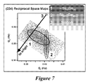
- FIG. 7 is a (224) reciprocal space maps of the 10 nm thick sample and the Si substrate, showing peaks [1] and [2] for the two layer structure.
- FIG. 8 shows an (Top) XTEM micrograph of the entire film thickness showing flat surface and bulk region devoid of defects; and (Bottom) a high resolution micrograph of the interface region showing perfect pseudomorphic growth.
- FIG. 9 shows (a) an XTEM micrograph of SiGe film (dark narrow band) grown selectively in the recessed “source” and “drain” areas of a device via deposition of Cl 2 Si(GeH 3 ) 2 at 420° C.
- the arrow indicates the height of the recess extending from the bottom of the trench up to the gate/channel interface (dotted line);
- FIG. 10 is a high-resolution XRD 2-D reciprocal space map of the (224) reflection of Si 0.33 Ge 0.67 in reciprocal lattice units (rlu) relative to the Si peak.
- the invention provides a method for the preparation of compounds of the molecular Formula (I), Si x Ge y H z-a X a (I) wherein x is 1, 2, 3, or 4; y is 1, 2, 3, or 4; z is 2(x+y+1); a is 1 to 3x; and X is halogen, provided that (i) each X is bonded only to Si; and (ii) the sum of x and y is less than or equal to 5, comprising the step of, treating a compound of the molecular Formula (II), Si x Ge y H z (II) with a compound of the formula BX 3 , AlX 3 , or a metal chlorinating agent, at a temperature of about ⁇ 80° C. to about 25° C.; such a method is referred to hereafter as Method A.
- compounds according to Formula (I) can be used, for example, in controlled depositions to produce stoichiometric Si d Ge 1-d films possessing desired properties for semiconductor applications including perfectly crystalline and epitaxial microstructures, smooth morphologies, and uniformly strain-relaxed states.
- the compounds of Formula (I) are herein demonstrated to be remarkably stable over extended periods of time, and thus represent viable molecular sources for potential industrial applications.
- Compounds according to this aspect of the invention include any conformational form of the compound, including but not limited n, g, and iso-forms of the compounds, and combinations thereof.
- Exemplary silicon-germanium hydrides starting materials of Formula (II) for the methods according to this aspect of the invention comprise or consist of those compounds listed in Table 1. All Si and Ge atoms in the compounds are tetravalent. In the isobutane- and isopentane-like isomers, the Si and Ge atoms inside the brackets are directly bound to the Si or Ge to the left of the brackets; the Si or Ge in parenthesis outside of the brackets at the far right in some of the compounds are directly bound to the last Si or Ge inside of the brackets.
- the invention provides the method of Method A, wherein for the compound of Formula (I), x, y, z, and a are according to one of the following (Table 2),
- X is chloro or bromo. In a preferred embodiment, X is chloro.
- a is 1. In another embodiment of Method A, a is 3x.
- x is 1 and a is 3. In another embodiment of Method A, x is 1 and a is 1. In another embodiment of Method A, x is 1 and a is 2.
- x is 2 and a is 6. In another embodiment of Method A, x is 2 and a is 1.
- x is 3 and a is 9. In another embodiment of Method A, x is 3 and a is 1.
- x is 4 and a is 12. In another embodiment of Method A, x is 4 and a is 1.
- the sum of x and y is less than or equal to 4. In another embodiment of Method A, the sum of x and y is less than or equal to 3. In another embodiment of Method A, the sum of x and y is 2.
- the compound of molecular Formula (I) is of formula (III), SiGe y H z-a X a (III) wherein y is 1, 2, 3, or 4; z is 2(y+2); a is 1 to 3; and X is halogen, provided that each X is bonded only to Si; such a method is referred to hereafter as Method B.
- X is chloro or bromo. In a preferred embodiment, X is chloro.
- y is 1. In another embodiment of Method B, y is 2. In another embodiment of Method B, y is 3. In another embodiment of Method B, y is 4.
- Method B a is 1. In another embodiment of Method B, a is 2. In another embodiment of Method B, a is 3.
- y is 1 and a is 1. In another preferred embodiment of Method B, y is 1 and a is 2. In another preferred embodiment of Method B, y is 1 and a is 3.
- the compound of formula (II) is H 3 SiGeH 3 , H 2 Si(GeH 3 ) 2 , or HSi(GeH 3 ) 3 .
- the compound of formula (II) is H 3 GeSiH 2 SiH 2 GeH 3 .
- the compound of formula (II) is H 3 SiGeH 3 , H 2 Si(GeH 3 ) 2 , or HSi(GeH 3 ) 3 and a is 1.
- the compound of formula (II) is H 3 SiGeH 3 or H 2 Si(GeH 3 ) 2 , and a is 2.
- the compound of formula (II) is H 3 GeSiH 2 SiH 2 GeH 3 and a is 1 or 2.
- the compound of molecular Formula (I) is of formula (IV), SiGe y H z-a Cl a (IV) wherein y is 1, 2, 3, or 4; z is 2(y+2); a is 1 to 3; and provided that each Cl is bonded only to Si; such a method is referred to hereafter as Method C.
- y is 1. In another embodiment of Method C, y is 2. In another embodiment of Method C, y is 3. In another embodiment of Method C, y is 4.
- a is 1. In another embodiment of Method C, a is 2. In another embodiment of Method C, a is 3.
- y is 1 and a is 1. In another preferred embodiment of Method C, y is 1 and a is 2. In another preferred embodiment of Method C, y is 1 and a is 3.
- the compound of formula (II) is H 3 SiGeH 3 , H 2 Si(GeH 3 ) 2 , or HSi(GeH 3 ) 3 .
- the compound of formula (II) is H 3 GeSiH 2 SiH 2 GeH 3 .
- the compound of formula (II) is H 3 SiGeH 3 , H 2 Si(GeH 3 ) 2 , or HSi(GeH 3 ) 3 and a is 1.
- the compound of formula (II) is H 3 SiGeH 3 or H 2 Si(GeH 3 ) 2 , and a is 2.
- the compound of formula (II) is H 3 GeSiH 2 SiH 2 GeH 3 and a is 1 or 2.
- the compound of molecular Formula (I) is of formula (V), SiGeH 6-a Cl a (V) wherein a is 1 to 3, provided that each Cl is bonded only to Si; such a method is referred to hereafter as Method D.
- the compound of molecular Formula (I) is of formula (VI), Si x GeH z-a X a (VI) wherein x is 1, 2, 3, or 4; z is 2(x+2); a is 1 to 3x; and X is halogen, provided that each X is bonded only to Si; such a method is referred to hereafter as Method E.
- X is chloro or bromo. In a preferred embodiment, X is chloro.
- x is 1. In another embodiment of Method E, x is 2. In another embodiment of Method E, x is 3. In another embodiment of Method E, x is 4.
- Method E In one embodiment of Method E, a is 1. In another embodiment of Method E, a is 2. In another embodiment of Method E, a is 3.
- x is 2 and a is 1. In another preferred embodiment of Method E, x is 3 and a is 1. In another preferred embodiment of Method E, x is 4 and a is 1.
- x is 2 and a is 2. In another preferred embodiment of Method E, x is 3 and a is 2. In another preferred embodiment of Method E, x is 4 and a is 2.
- the compound of molecular Formula (I) is of formula (VII), Si x GeH z-a Cl a (VII) wherein x is 1, 2, 3, or 4; z is 2(x+2); a is 1 to 3x; and provided that each Cl is bonded only to Si; such a method is referred to hereafter as Method F.
- x is 1. In another embodiment of Method F, x is 2. In another embodiment of Method F, x is 3. In another embodiment of Method F, x is 4.
- Method F In one embodiment of Method F, a is 1. In another embodiment of Method F, a is 2. In another embodiment of Method F, a is 3.
- x is 1 and a is 1. In another preferred embodiment of Method F, x is 2 and a is 1. In another preferred embodiment of Method F, x is 3 and a is 1. In another preferred embodiment of Method F, x is 4 and a is 1.
- x is 1 and a is 2. In another preferred embodiment of Method F, x is 2 and a is 2. In another preferred embodiment of Method F, x is 3 and a is 2. In another preferred embodiment of Method F, x is 4 and a is 2.
- the invention provides the method of any one of Methods A-F, further comprising the step of
- step (ii) fractionally distilling the product of step (i).
- the invention provides the method of any one of Methods A-F, the compound of molecular Formula (I) is treated with a compound of the formula BX 3 .
- the compound is BCl 3 or BBr 3 . More preferably, the compound is BCl 3 .
- the invention provides the method of any one of Methods A-F, wherein the reaction temperature is about ⁇ 60° C. to about 10° C. In a preferred embodiment of the first aspect, the invention provides the method of any one of Methods A-F, wherein the reaction temperature is about ⁇ 25° C. to about 5° C.
- the invention provides the method of any one of Methods A-F, wherein the compound of Formula (I) is
- the invention provides a method for the preparation of compounds of the molecular formula (XII), Si x Ge y H z-1 X (XII) wherein x is 1, 2, 3, or 4; y is 1, 2, 3, or 4; z is 2(x+y+1); a is 1 to 3x; and X is halogen, provided that (i) X is bonded only to Si; and (ii) the sum of x and y is less than or equal to 5, comprising the steps of,
- Method G a method of the formula CsX at a temperature of about ⁇ 50° C. to about 40° C.
- x is 1. In another embodiment of Method G, x is 1 and y is 1. In another embodiment of Method G, x is 1 and y is 2. In another embodiment of Method G, x is 1 and y is 3. In another embodiment of Method G, x is 1 and y is 4.
- X is chloro
- the invention provides a method for the preparation of compounds of formula (XIV), SiGe y H z-1 X (XIV) wherein y is 1, 2, 3, or 4; z is 2(y+2); and X is halogen, provided that X is bonded only to Si; comprising the steps of,
- y is 1. In another embodiment of Method H, y is 2. In another embodiment of Method H, y is 3. In another embodiment of Method H, y is 4.
- X is chloro
- the invention provides a method for the preparation of ClH 2 SiGeH 3 , comprising the steps of,
- y is 1. In another embodiment of Method I, y is 2. In another embodiment of Method I, y is 3. In another embodiment of Method I, y is 4.
- the invention provides a method for the preparation of compounds of formula (XVI), SiGe y H z-1 Cl (XVI) wherein y is 1, 2, 3, or 4; z is 2(y+2); and provided that Cl is bonded only to Si; comprising the steps of,
- y is 1. In another embodiment of Method J, y is 2. In another embodiment of Method J, y is 3. In another embodiment of Method J, y is 4.
- the invention provides a method for the preparation of the compound, ClH 2 SiGeH, comprising the steps of, (i) contacting a compound of the formula YH 2 SiGeH 3 , wherein Y is —OSO 2 R 1 , wherein R 1 is C 1 -C 6 haloalkyl, C 1 -C 6 alkyl, or phenyl, wherein the alkyl and phenyl are optionally substituted with 1 to 4 groups which are each independently halogen, C 1 -C 2 haloalkyl, C 1 -C 3 alkyl, cyano, nitro, C 1 -C 3 alkoxy, —C(O)C 1 -C 3 alkoxy, —C(O)C 1 -C 3 alkyl, —S(O)C 1 -C 3 alkyl, or —S(O) 2 C 1 -C 3 alkyl, provided that Y is bonded only to Si; with
- R 1 is C 1 -C 6 haloalkyl, C 1 -C 6 alkyl, or phenyl, wherein phenyl are optionally substituted with halogen, C 1 -C 2 haloalkyl, C 1 -C 3 alkyl, cyano, nitro, C 1 -C 3 alkoxy, —C(O)C 1 -C 3 alkoxy, —C(O)C 1 -C 3 alkyl, —S(O)C 1 -C 3 alkyl, or —S(O) 2 C 1 -C 3 alkyl.
- R 1 is C 1 -C 4 haloalkyl, C 1 -C 4 alkyl, or phenyl, wherein phenyl is optionally substituted with halogen, C 1 -C 2 haloalkyl, or C 1 -C 3 alkyl.
- R 1 is C 1 -C 4 perfluoroalkyl, C 1 -C 4 alkyl, or phenyl, wherein phenyl is optionally substituted with halogen, C 1 -C 2 perfluoroalkyl, or C 1 -C 3 alkyl.
- the invention provides the method of any one of Methods G-K, wherein the reaction temperature is about ⁇ 25° C. to about 25° C.
- the invention provides the method of any one of Methods G-K, further comprising the step of
- the invention provides a method for the preparation of compounds of the molecular Formula (XVII), Si x Ge y H z-a X a (XVII) wherein x is 1, 2, 3, or 4; y is 1, 2, 3, or 4; z is 2(x+y+1); a is 1 to z; and X is halogen, provided that the sum of x and y is less than or equal to 5, comprising the step of, treating a compound of the molecular Formula (LX), Si x Ge y H z (LX) with a compound of the formula BX 3 or AlX 3 at a temperature of about ⁇ 80° C. to about 25° C.; such a method is referred to hereafter as Method A1.
- compounds according to Formula (XVII) can be used, for example, in controlled depositions to produce stoichiometric Si d Ge 1-d films possessing desired properties for semiconductor applications including perfectly crystalline and epitaxial microstructures, smooth morphologies, and uniformly strain-relaxed states.
- the compounds of Formula (XVII) are herein demonstrated to be remarkably stable over extended periods of time, and thus represent viable molecular sources for potential industrial applications.
- Compounds according to this aspect of the invention include any conformational form of the compound, including but not limited n, g, and iso-forms of the compounds, and combinations thereof.
- Exemplary silicon-germanium hydrides starting materials of Formula (LX) for the methods according to this aspect of the invention comprise or consist of those compounds listed in Table 1.
- the invention provides the method of Method A1, wherein for the compound of Formula (I), x, y, z, and a are according to listed in Table 2 or one of the following (Table 3),
- X is chloro or bromo. In a preferred embodiment, X is chloro.
- a is 1. In another embodiment of Method A1, a is 1 to 2(x+y). In another embodiment of Method A1, a is 2(x+y).
- the sum of x and y is less than or equal to 4. In another embodiment of Method A1, the sum of x and y is less than or equal to 3. In another embodiment of Method A1, the sum of x and y is 2.
- each Si and Ge atom has no more than two X bonded thereto.
- a is 1 to 2(x+y) and each Si and Ge atom has no more than two X bonded thereto.
- the compound of molecular Formula (XVII) is of formula (XVIII), SiGe y H z-a X a (XVIII) wherein y is 1, 2, 3, or 4; z is 2(y+2); a is 1 to z; and X is halogen, such a method is referred to hereafter as Method B1.
- X is chloro or bromo. In a preferred embodiment, X is chloro.
- Method B1 a is 1. In another embodiment of Method B1, a is 1 to 2(1+y). In another embodiment of Method B1, a is 2(1+y).
- y is 1, 2, or 3. In another embodiment of Method B1, y is 1 or 2. In another embodiment of Method B1, y is 1.
- each Si and Ge atom has no more than two X bonded thereto.
- a is 1 to 2(1+y) and each Si and Ge atom has no more than two X bonded thereto.
- the compound of formula (LX) is H 3 SiGeH 3 , H 2 Si(GeH 3 ) 2 , or HSi(GeH 3 ) 3 .
- the compound of formula (LX) is H 3 GeSiH 2 SiH 2 GeH 3 .
- the compound of formula (LX) is H 3 SiGeH 3 , H 2 Si(GeH 3 ) 2 , or HSi(GeH 3 ) 3 and a is 1.
- the compound of formula (LX) is H 3 SiGeH 3 , H 2 Si(GeH 3 ) 2 , or HSi(GeH 3 ) 3 , and a is 2 or 3.
- the compound of formula (LX) is H 3 GeSiH 2 SiH 2 GeH 3 and a is 1 or 2.
- the compound of molecular Formula (XVII) is of formula (XIX), SiGe y H z-a Cl a (XIX) wherein y is 1, 2, 3, or 4; z is 2(y+2); a is 1 to z; such a method is referred to hereafter as Method Cl.
- a is 1. In another embodiment of Method C1, a is 1 to 2(1+y). In another embodiment of Method C1, a is 2(1+y).
- y is 1, 2, or 3. In another embodiment of Method C1, y is 1 or 2. In another embodiment of Method C1, y is 1.
- each Si and Ge atom has no more than two X bonded thereto.
- a is 1 to 2(1+y) and each Si and Ge atom has no more than two X bonded thereto.
- the compound of formula (LX) is H 3 SiGeH 3 , H 2 Si(GeH 3 ) 2 , or HSi(GeH 3 ) 3 .
- the compound of formula (LX) is H 3 GeSiH 2 SiH 2 GeH 3 .
- the compound of formula (LX) is H 3 SiGeH 3 , H 2 Si(GeH 3 ) 2 , or HSi(GeH 3 ) 3 and a is 1.
- the compound of formula (LX) is H 3 SiGeH 3 , H 2 Si(GeH 3 ) 2 , or HSi(GeH 3 ) 3 , and a is 2, 3, or 4.
- the compound of formula (LX) is H 3 GeSiH 2 SiH 2 GeH 3 and a is 1, 2, 3, or 4.
- the compound of molecular Formula (XVII) is of formula (XX), SiGeH 6-a Cl a (XX) wherein a is 1 to z; such a method is referred to hereafter as Method D1.
- Method D1 In one embodiment of Method D1, a is 1 to 4. In another embodiment of Method D1, a is 2. In another embodiment of Method D1, a is 1. In another embodiment of Method D1, a is 4.
- each Si and Ge atom has no more than two X bonded thereto.
- a is 1 to 4 and each Si and Ge atom has no more than two X bonded thereto.
- the compound of molecular Formula (XVII) is of formula (XXI), Si x GeH z-a X a (XXI) wherein x is 1, 2, 3, or 4; z is 2(x+2); a is 1 to z; and X is halogen; such a method is referred to hereafter as Method E1.
- X is chloro or bromo. In a preferred embodiment, X is chloro.
- a is 1. In another embodiment of Method E1, a is 1 to 2(x+1). In another embodiment of Method E1, a is 2(x+1).
- x is 1, 2, or 3. In another embodiment of Method E1, x is 1 or 2. In another embodiment of Method E1, x is 1.
- each Si and Ge atom has no more than two X bonded thereto.
- a is 1 to 2(x+1) and each Si and Ge atom has no more than two X bonded thereto.
- the compound of molecular Formula (XVII) is of formula (XXII), Si x GeH z-a Cl a (XXII) wherein x is 1, 2, 3, or 4; z is 2(x+2); a is 1 to 3x; and provided that each C1 is bonded only to Si; such a method is referred to hereafter as Method F1.
- Method F1 In one embodiment of Method F1, a is 1. In another embodiment of Method F1, a is 1 to 2(x+1). In another embodiment of Method F1, a is 2(x+1).
- x is 1, 2, or 3. In another embodiment of Method F1, x is 1 or 2. In another embodiment of Method F1, x is 1.
- each Si and Ge atom has no more than two X bonded thereto.
- a is 1 to 2(x+1) and each Si and Ge atom has no more than two X bonded thereto.
- the invention provides the method of any one of Methods A1-F1, further comprising the step of
- step (ii) fractionally distilling the product of step (i).
- the invention provides the method of any one of Methods A1-F1, the compound of any of molecular Formulas (XVII)-(XXII) is treated with a compound of the formula BX 3 .
- the compound is BCl 3 or BBr 3 . More preferably, the compound is BCl 3 .
- the invention provides the method of any one of Methods A1-F1, wherein the reaction temperature is about ⁇ 60° C. to about 10° C. In a preferred embodiment of the third aspect, the invention provides the method of any one of Methods A1-F1, wherein the reaction temperature is about ⁇ 25° C. to about 5° C.
- the invention provides the method of any one of Methods A1-F1, wherein the compound of Formula (XVII) is
- the invention provides the compounds of any of Formulas (I)-(XXII) prepared according to any of the preceding embodiments of the first, second, and third aspects.
- the invention provides the substantially pure compound of any of Formulas (I)-(XXII) prepared according to any embodiment of any of the preceding aspects of the invention.
- the invention provides the substantially pure compound of formula (III) or (XVIII) prepared according to any of the preceding embodiments.
- the invention provides the substantially pure compound of formula (XIV) prepared according to any of the preceding embodiments.
- the invention provides the substantially pure compound of formula (IV) or (XIX) prepared according to any of the preceding embodiments.
- the invention provides the substantially pure compound of formula (XVI) prepared according to any of the preceding embodiments.
- the invention provides the substantially pure compound of formula (V) or (XX) prepared according to any of the preceding embodiments.
- the invention provides the substantially pure compound of formula (VI) or (XXI) prepared according to any of the preceding embodiments.
- the invention provides the substantially pure compound of formula (VII) or (XXII) prepared according to any of the preceding embodiments.
- the invention provides the substantially pure compound which is chloro(germyl)silane or dichloro(germyl)silane, prepared according to any of the preceding embodiments.
- the invention provides a method for preparing a layer of the formula, Si d Ge 1-d , wherein d is greater than 0 and less than 1, on a substrate, comprising:
- Method L contacting the substrate with a chemical vapor comprising a compound of the molecular formula, Si x Ge y H z-a X a (I) wherein x is 1, 2, 3, or 4; y is 1, 2, 3, or 4; z is 2(x+y+1); a is Ito 3x; and X is halogen, provided that (i) each X is bonded only to Si; and (ii) the sum of x and y is less than or equal to 5; such method is referred to hereafter as Method L.
- X is chloro or bromo. In a preferred embodiment, X is chloro.
- Method L In one embodiment of Method L, a is 1. In another embodiment of Method L, a is 3x.
- x is 1 and a is 3. In another embodiment of Method L, x is 1 and a is 1. In another embodiment of Method L, x is 1 and a is 2.
- x is 2 and a is 6. In another embodiment of Method L, x is 2 and a is 1. In another embodiment of Method L, x is 2 and a is 2.
- Method L In another embodiment of Method L, In another embodiment of Method L, x is 2, y is 1, and a is 1. In another embodiment of Method L, x is 2, y is 1, and a is 2. In another embodiment of Method L, x is 2, y is 1, and a is 3. In another embodiment of Method L, x is 2, y is 1, and a is 4.
- Method L In another embodiment of Method L, In another embodiment of Method L, x is 2, y is 2, and a is 1. In another embodiment of Method L, x is 2, y is 2, and a is 2. In another embodiment of Method L, x is 2, y is 2, and a is 3. In another embodiment of Method L, x is 2, y is 2, and a is 4.
- x is 3 and a is 9. In another embodiment of Method L, x is 3 and a is 1. In another embodiment of Method L, x is 3 and a is 2. In another embodiment of Method L, x is 3 and a is 3.
- x is 3 and y is 2. In another embodiment of Method L, x is 3, y is 2, and a is 1. In another embodiment of Method L, x is 3, y is 2 and a is 2. In another embodiment of Method L, x is 3, y is 2, and a is 3, 4, 5, or 6.
- x is 4 and a is 12. In another embodiment of Method L, x is 4 and a is 1. In another embodiment of Method L, x is 4 and a is 2. In another embodiment of Method L, x is 4 and a is 3. In another embodiment of Method L, x is 4 and a is 4.
- the sum of x and y is less than or equal to 4. In another embodiment of Method L, the sum of x and y is less than or equal to 3. In another embodiment of Method L, the sum of x and y is 2.
- the chemical vapor comprises a compound of the formula (III), SiGe y H z-a X a (III) wherein y is 1, 2, 3, or 4; z is 2(y+2); a is 1 to 3; and X is halogen, provided that each X is bonded only to Si; such method is referred to hereafter as Method M.
- X is chloro or bromo. In a preferred embodiment, X is chloro.
- y is 1. In another embodiment of Method M, y is 2. In another embodiment of Method M, y is 3. In another embodiment of Method M, y is 4.
- Method M In one embodiment of Method M, a is 1. In another embodiment of Method M, a is 2. In another embodiment of Method M, a is 3.
- y is 1 and a is 1. In another preferred embodiment of Method M, y is 1 and a is 2. In another preferred embodiment of Method M, y is 1 and a is 3.
- y is 2 and a is 1. In another preferred embodiment of Method M, y is 2 and a is 2.
- y is 3 and a is 1.
- the chemical vapor comprises a compound of formula (IV), SiGe y H z-a Cl a (IV) wherein y is 1, 2, 3, or 4; z is 2(y+2); a is 1 to 3; and provided that each C1 is bonded only to Si, such a method is referred to hereafter as Method N.
- y is 1. In another embodiment of Method N, y is 2. In another embodiment of Method N, y is 3. In another embodiment of Method N, y is 4.
- Method N a is 1. In another embodiment of Method N, a is 2. In another embodiment of Method N, a is 3.
- y is 1 and a is 1. In another preferred embodiment of Method N, y is 1 and a is 2. In another preferred embodiment of Method N, y is 1 and a is 3.
- y is 2 and a is 1. In another preferred embodiment of Method N, y is 2 and a is 2.
- y is 3 and a is 1.
- the chemical vapor comprises a compound of formula (V), SiGeH 6-a Cl a (V) wherein a is 1 to 3; and provided that each Cl is bonded only to Si, such a method is referred to hereafter as Method O.
- the chemical vapor comprises a compound of the formula (VI), Si x GeH z-a X a (VI) wherein x is 1, 2, 3, or 4; z is 2(x+2); a is 1 to 3x; and X is halogen, provided that each X is bonded only to Si; such method is referred to hereafter as Method P.
- X is chloro or bromo. In a preferred embodiment, X is chloro.
- x is 1. In another embodiment of Method P, x is 2. In another embodiment of Method P, x is 3. In another embodiment of Method P, x is 4.
- Method P In one embodiment of Method P, a is 1. In another embodiment of Method P, a is 2. In another embodiment of Method P, a is 3.
- x is 2 and a is 1. In another preferred embodiment of Method P, x is 3 and a is 1. In another preferred embodiment of Method P, x is 4 and a is 1.
- x is 2 and a is 2. In another preferred embodiment of Method P, x is 3 and a is 2. In another preferred embodiment of Method P, x is 4 and a is 2.
- the chemical vapor comprises a compound of formula (VII), Si x GeH z-a Cl a (VII) wherein x is 1, 2, 3, or 4; z is 2(x+2); a is 1 to 3x; and provided that each Cl is bonded only to Si, such a method is referred to hereafter as Method Q.
- x is 1. In another embodiment of Method Q, x is 2. In another embodiment of Method Q, x is 3. In another embodiment of Method Q, x is 4.
- Method Q a is 1. In another embodiment of Method Q, a is 2. In another embodiment of Method Q, a is 3.
- x is 1 and a is 1. In another preferred embodiment of Method Q, x is 2 and a is 1. In another preferred embodiment of Method Q, x is 3 and a is 1. In another preferred embodiment of Method Q, x is 4 and a is 1.
- x is 1 and a is 2. In another preferred embodiment of Method Q, x is 2 and a is 2. In another preferred embodiment of Method Q, x is 3 and a is 2. In another preferred embodiment of Method Q, x is 4 and a is 2.
- the chemical vapor comprises a compound which is
- the invention provides a method for preparing a substantially crystalline layer of the formula, Si d Ge 1-d , wherein d is greater than 0 and less than 1, on a substrate, comprising:
- Method L1 a chemical vapor comprising a compound of the molecular formula, Si x Ge y H z-a X a (XVII) wherein x is 1, 2, 3, or 4; y is 1, 2, 3, or 4; z is 2(x+y+1); a is 1 to z; and X is halogen, provided that the sum of x and y is less than or equal to 5; such method is referred to hereafter as Method L1.
- X is chloro or bromo. In a preferred embodiment, X is chloro.
- Method L1 In one embodiment of Method L1, a is 1. In another embodiment of Method L1, a is 1 to 2(x+y). In another embodiment of Method L1, a is 2(x+y).
- the sum of x and y is less than or equal to 4. In another embodiment of Method L1, the sum of x and y is less than or equal to 3. In another embodiment of Method L1, the sum of x and y is 2.
- each Si and Ge atom has no more than two X bonded thereto.
- a is 1 to 2(x+y) and each Si and Ge atom has no more than two X bonded thereto.
- the chemical vapor comprises a compound of the formula (XVIII), SiGe y H z-a X a (XVIII) wherein y is 1, 2, 3, or 4; z is 2(y+2); a is 1 to 3; and X is halogen, provided that each X is bonded only to Si; such method is referred to hereafter as Method M1.
- X is chloro or bromo. In a preferred embodiment, X is chloro.
- Method M1 In one embodiment of Method M1, a is 1. In another embodiment of Method M1, a is 1 to 2(1+y). In another embodiment of Method M1, a is 2(1+y).
- y is 1, 2, or 3. In another embodiment of Method M1, y is 1 or 2. In another embodiment of Method M1, y is 1. In another embodiment of Method M1, y is 2.
- Method M1 y is 1 and a is 1. In another embodiment of Method M1, y is 1 and a is 2. In another embodiment of Method M1, y is 2. In another embodiment of Method M1, y is 2 and a is 1. In another embodiment of Method M1, y is 2 and a is 2.
- each Si and Ge atom has no more than two X bonded thereto.
- a is 1 to 2(1+y) and each Si and Ge atom has no more than two X bonded thereto.
- the chemical vapor comprises a compound of formula (XIX), SiGe y H z-a Cl a (XIX) wherein y is 1, 2, 3, or 4; z is 2(y+2); a is 1 to 3; and provided that each Cl is bonded only to Si, such a method is referred to hereafter as Method N1.
- Method N1 a is 1. In another embodiment of Method N1, a is 1 to 2(1+y). In another embodiment of Method N1, a is 2(1+y).
- y is 1, 2, or 3. In another embodiment of Method N1, y is 1 or 2. In another embodiment of Method N1, y is 1. In another embodiment of Method N1, y is 2.
- y is 1 and a is 1. In another embodiment of Method N1, y is 1 and a is 2. In another embodiment of Method N1, y is 2. In another embodiment of Method N1, y is 2 and a is 1. In another embodiment of Method N1, y is 2 and a is 2.
- each Si and Ge atom has no more than two X bonded thereto.
- a is 1 to 2(1+y) and each Si and Ge atom has no more than two X bonded thereto.
- the chemical vapor comprises a compound of formula (XX), SiGeH 6-a Cl a (XX) wherein a is 1 to 3; and provided that each Cl is bonded only to Si, such a method is referred to hereafter as Method O1.
- a is 1. In another embodiment of Method O1, a is 1 to 4. In another embodiment of Method O1, a is 4.
- each Si and Ge atom has no more than two X bonded thereto.
- a is 1 to 4 and each Si and Ge atom has no more than two X bonded thereto.
- the chemical vapor comprises a compound of the formula (XXI), Si x GeH z-a X a (XXI) wherein x is 1, 2, 3, or 4; z is 2(x+2); a is 1 to 3x; and X is halogen, provided that each X is bonded only to Si; such method is referred to hereafter as Method P1.
- X is chloro or bromo. In a preferred embodiment, X is chloro.
- a is 1. In another embodiment of Method P1, a is 1 to 2(x+1). In another embodiment of Method P1, a is 2(x+1).
- x is 1, 2, or 3. In another embodiment of Method P1, x is 1 or 2. In another embodiment of Method P1, x is 1.
- each Si and Ge atom has no more than two X bonded thereto.
- a is 1 to 2(x+1) and each Si and Ge atom has no more than two X bonded thereto.
- the chemical vapor comprises a compound of formula (XXII), Si x GeH z-a Cl a (XXII) wherein x is 1, 2, 3, or 4; z is 2(x+2); a is 1 to 3x; and provided that each Cl is bonded only to Si, such a method is referred to hereafter as Method Q1.
- Method Q1 In one embodiment of Method Q1, a is 1. In another embodiment of Method Q1, a is 1 to 2(x+1). In another embodiment of Method Q1, a is 2(x+1).
- x is 1, 2, or 3. In another embodiment of Method Q1, x is 1 or 2. In another embodiment of Method Q1, x is 1.
- each Si and Ge atom has no more than two X bonded thereto.
- a is 1 to 2(x+1) and each Si and Ge atom has no more than two X bonded thereto.
- d is about 0.2 to about 0.5. In a preferred embodiment of any one of Methods L-N or L1-N1 and preferred embodiments thereof, d is about 0.2. In a preferred embodiment of any one of Methods L-N or L1-N1 and preferred embodiments thereof, d is about 0.25. In a preferred embodiment any one of Methods L-N or L1-N1 and preferred embodiments thereof, d is about 0.33. In a preferred embodiment of Methods any one of Methods L-Q or L1-Q1 and preferred embodiments thereof, d is about 0.50.
- the deposited layer of the formula Si d Ge 1-d has the same empirical formula for silicon and germanium as the compound of Formula (I) or (XVII), e.g. wherein the layer is deposited using a compound of Formula (I), Si x Ge y H z-a X a , the deposited layer has an empirical formula of Si x Ge y .
- the deposited layer when the layer is deposited using a compound of formula (III) or (XVIII), SiGe y H z-a X a , the deposited layer has an empirical formula of SiGe y .
- the deposited layer when the layer is deposited using a compound of formula (IV) or (XIX), SiGe y H z-a Cl a , the deposited layer has an empirical formula of SiGe y . In a preferred embodiment, when the layer is deposited using a compound of formula (V) or (XX), SiGeH 6-a Cl a , the deposited layer has an empirical formula of SiGe. In a preferred embodiment, when the layer is deposited using a compound of formula (VI) or (XXI), Si x GeH z-a X a , the deposited layer has an empirical formula of Si x Ge. In a preferred embodiment, when the layer is deposited using a compound of formula (VII) or (XXII), Si x GeH z-a Cl a , the deposited layer has an empirical formula of Si x Ge.
- the chemical vapor comprises a compound which is
- the deposited layer has an empirical formula of SiGe.
- the temperature is from about 200° C. to about 600° C. More preferably, the temperature is about 350° C. to about 450° C. Even more preferably, the temperature is about 400° C. to about 450° C.
- the layer is substantially crystalline.
- the layer is substantially crystalline and the temperature is from about 200° C. to about 600° C. More preferably, the layer is substantially crystalline and the temperature is about 350° C. to about 450° C. Even more preferably, the layer is substantially crystalline and the temperature is about 400° C. to about 450° C.
- the substrate comprises any substrate suitable for semiconductor or flat panel display use, including but not limited to silicon, germanium, silicon on insulator, Ge:Sn alloys, SiO 2 , sapphire, quartz, Si:Ge alloys, Si:C alloys, stainless steel, polyimide or other polymer films such as those used in the fabrication of flexible displays.
- the substrate comprises silicon.
- the substrate comprises Si(100).
- the compound of any one of Formulas (I)-(XXII) can be deposited by any suitable technique, including but not limited to gas source molecular beam epitaxy, chemical vapor deposition, plasma enhanced chemical vapor deposition, laser assisted chemical vapor deposition, and atomic layer deposition.
- the compound of any one of Formulas (I)-(XXII) is introduced at a partial pressure between about 10 ⁇ 8 Torr and 760 Torr.
- the chemical vapor is introduced at between 10 ⁇ 8 Torr and 10 ⁇ 5 Torr (corresponding to UHV vertical furnace technology).
- the chemical vapor is introduced at between 10 ⁇ 8 Torr and 100 Torr, corresponding to LPCVD conditions.
- the chemical vapor is introduced at between 10 ⁇ 3 Torr and 760 Torr.
- the compound of any one of Formulas (I)-(XXII) can be deposited under plasma-enhanced chemical vapor deposition (PECVD) conditions.
- PECVD plasma-enhanced chemical vapor deposition
- PECVD is a process to deposit thin films from a gas state (vapor) to a solid state on a substrate.
- the reactive chemical species involved in the process are generated by the creation of a plasma from the reacting gases.
- the plasma is generally created by RF (AC) frequency or DC discharge between two electrodes.
- PECVD process parameters include flow rate, F, in standard cubic centimeters per minute (sccm), applied power, W, in Watts (W), resonant frequency in kilohertz (kHz), pressure in milliTorr (mTorr), substrate temperature in Celsius degrees (° C.) and geometrical factors such as size of chamber, electrode size, electrode orientation and distance from substrate, etc.
- the composite parameter, W/FM, or energy per unit mass of monomer was also used in this study. This composite parameter, expressed in MJ/kg, is calculated from the following expression
- W / FM ⁇ ( MJ / kg ) W ⁇ ( Watt ) F ⁇ ( sccm ) ⁇ M ⁇ ( g ⁇ / ⁇ mol ) ⁇ 1340 whereby M is the molecular weight of the precursor in g/mol.
- the substrate temperature is about 20° C. to about 600° C. More preferably, the temperature is about 20° C. to about 300° C. Even more preferably, the temperature is about 20° C. to about 250° C.
- the composite plasma parameter W/FM is ⁇ about 200 MJ/kg; more preferably ⁇ 100 MJ/kg, and even more preferably ⁇ 30 MJ/kg.
- the Si—Ge material is formed on the substrate as a partially to fully strain-relaxed layer having a planar surface; the composition of the Si—Ge material is substantially uniform; and/or the entire Si and Ge framework of the chemical vapor is incorporated into the Si—Ge material or epitaxial Si—Ge.
- the Si—Ge material is formed on the substrate as fully strained layer having a planar surface; the composition of the Si—Ge material is substantially uniform; and/or the entire Si and Ge framework of the chemical vapor is incorporated into the Si—Ge material or epitaxial Si—Ge.
- the substantially crystalline Si—Ge material is formed on the substrate has a substantially single crystalline domain.
- the invention provides a compound according to formula (XXIV), Si x Ge y H z-a X a (XXIV) wherein x is 1, 2, 3, or 4; y is 1, 2, 3, or 4; z is 2(x+y+1); a is 1 to 2(x+y), and X is halogen, provided that (i) the sum of x and y is less than or equal to 5; (ii) each Si and Ge atom has no more than two X groups bonded thereto; and (iii) the compound is not
- the invention provides the compound of formula (XXIV), wherein a is 1. In another embodiment the invention provides the compound of formula (XXIV), wherein a is 2(x+y).
- the invention provides the compound of formula (XXIV), wherein X is chloro or bromo. In a preferred embodiment, X is chloro.
- the invention provides the compound of formula (XXIV), wherein the sum of x and y is less than or equal to 4. In another embodiment the invention provides the compound of formula (XXIV), wherein the sum of x and y is less than or equal to 3. In another embodiment the invention provides the compound of formula (XXIV), wherein the sum of x and y is 2.
- the compound of Formula (XXIV) is of molecular formula (XXV), SiGe y H z-a X a (XXV) wherein y is 1, 2, 3, or 4; z is 2(y+2); a is 1 to 2(1+y); and X is halogen.
- X is chloro or bromo. In a preferred embodiment, X is chloro.
- a is 1. In another embodiment of Formula (XXV), a is 2(1+y).
- Formula (XXV) y is 1, 2, or 3. In another embodiment of Formula (XXV), y is 1 or 2. In another embodiment of Formula (XXV), y is 1.
- the compound of molecular Formula (XXV) is of formula (XXVI), SiGe y H z-a Cl a (XXVI) wherein y is 1, 2, 3, or 4; z is 2(y+2); a is Ito 2(1+y).
- a is 1. In another embodiment formula (XXVI), a is 2(1+y).
- formula (XXVI) y is 1, 2, or 3. In another embodiment of formula (XXVI), y is 1 or 2. In another embodiment of formula (XXVI), y is 1.
- the compound of molecular Formula (XXVI) is of formula (XXVII), SiGeH 6-a Cl a (XXVII) wherein a is 1 to 4.
- a is 1. In another embodiment of formula (XXVII), a is 4.
- the compound is of formula (XXVIII), Si x GeH z-a X a (XXVIII) wherein x is 1, 2, 3, or 4; z is 2(x+2); a is 1 to 2(x+1); and X is halogen.
- X is chloro or bromo. In a preferred embodiment, X is chloro.
- a is 1. In another embodiment of formula (XXVIII), a is 2(x+1).
- x is 1, 2, or 3. In another embodiment of formula (XXVIII), x is 1 or 2. In another embodiment of formula (XXVIII), x is 1.
- the compound of molecular Formula (XXVIII) is of formula (XXIX), Si x GeH z-a Cl a (XXIX) wherein x is 1, 2, 3, or 4; z is 2(x+2); a is Ito 2(x+1).
- a is 1. In another embodiment of formula (XXIX), a is 2(x+1).
- x is 1, 2, or 3. In another embodiment of formula (XXIX), x is 1 or 2. In another embodiment of formula (XXIX), x is 1.
- the invention provides the compound according to formula (XXIV) which is,
- the invention provides a substantially pure compound according to formula (XXIII), SiGe y H z-a Cl a (XXIII) wherein y is 1, 2, 3, or 4; z is 2(y+2); and a is 1 to 2(y+1), provided that each Si and Ge atom has no more than two X groups bonded thereto.
- the invention provides the substantially pure compound of formula (XXIII), wherein a is 1. In a preferred embodiment, the invention provides the substantially pure compound of formula (XXIII), wherein a is 2.
- the invention provides the substantially pure compound of formula (XXIII), wherein y is 1. In a preferred embodiment, the invention provides the substantially pure compound of formula (XXIII), wherein y is 2. In a preferred embodiment, the invention provides the substantially pure compound of formula (XXIII), wherein y is 3. In a preferred embodiment, the invention provides the substantially pure compound of formula (XXIII), wherein y is 4.
- the invention provides the substantially pure compound according to formula (XXIII), wherein y is 1 and a is 1. In a more preferred embodiment, the invention provides the substantially pure compound according to formula (XXIII), wherein y is 2 and a is 1. In a more preferred embodiment, the invention provides the substantially pure compound according to formula (XXIII), wherein y is 3 and a is 1. In a more preferred embodiment, the invention provides the substantially pure compound according to formula (XXIII), wherein y is 4 and a is 1.
- the invention provides the substantially pure compound according to formula (XXIII), wherein y is 1 and a is 2. In a more preferred embodiment, the invention provides the substantially pure compound according to formula (XXIII), wherein y is 2 and a is 2. In a more preferred embodiment, the invention provides the substantially pure compound according to formula (XXIII), wherein y is 3 and a is 2. In a more preferred embodiment, the invention provides the substantially pure compound according to formula (XXIII), wherein y is 4 and a is 2.
- the invention provides the substantially pure compound according to formula (XXIII), which is chloro(germyl)silane or dichloro(germyl)silane.
- the halosilylgermane compounds of any of Formulas (I)-(XXIV) are especially useful for fabricating Si d Ge 1-d semiconductor alloys at unprecedented low temperatures that display homogeneous compositional and strain profiles, low threading dislocation densities and atomically planar surfaces.
- Controlled depositions have produced stoichiometric Si d Ge 1-d films reflecting the Si/Ge content of the precursor, and possessing the desired properties for semiconductor applications including perfectly crystalline and epitaxial microstructures, smooth morphologies, and uniformly strain-relaxed states.
- Controlled depositions have also produced stoichiometric Si d Ge 1-d films reflecting the Si/Ge content of the precursor, and possessing perfectly crystalline and epitaxial microstructures, smooth morphologies, and fully strained states.
- the semiconductor substrates of this aspect of the invention have a deposited Si d Ge 1-d layer which comprises a Si d Ge 1-d film having a thickness of less than one micron, more preferably a thickness in a range from 50 nm to 500 nm.
- the semiconductor substrates of this second aspect have an Si d Ge 1-d layer comprising an Si d Ge 1-d film having a density of threading defects of 10 6 /cm 2 or less.
- the semiconductor substrates of this aspect of the invention comprise an Si d Ge 1-d film having a substantially atomically planar surface morphology.
- the chemical vapor comprises or consists of one or more of the compounds listed in Table 2, each in n or g forms, and stereoisomers thereof.
- the semiconductor structure may further comprise other features as desired, including but not limited to the inclusion of dopants, such as boron, phosphorous, arsenic, and antimony. These embodiments are especially preferred for semiconductor substrates used as active devices. Inclusion of such dopants into the semiconductor substrates can be carried out by standard methods in the art.
- dopants such as boron, phosphorous, arsenic, and antimony.
- the semiconductor structure may further comprise varying quantities if carbon or tin, as desired for a given application.
- Inclusion of carbon or tin into the semiconductor substrates can be carried out by standard methods in the art.
- the carbon can be used to reduce the mobility of the dopants in the structure and more specifically boron.
- Incorporation of Sn can yield materials with novel optical properties such as direct emission and absorption leading to the formation of Si-based lasers and high sensitivity infrared photodetectors.
- the invention provides a chemical vapor, comprising one or more compounds according to any of Formulas (I)-(XXIV) and a second gas.
- second gases include, but are not limited to, H 2 , He, N 2 , argon, and mixtures thereof; preferably, the second gas comprises H 2 .
- Preferred embodiments are as described above.
- the semiconductor substrate will comprise an Si—Ge layer comprising or consisting of a backbone of the compounds of the invention.
- the resulting Si—Ge layer comprises highly defined and uniform bonding arrangements and strain compensated Si—Ge atomic patterns, as opposed to the random nature of prior Si—Ge films in which the Si and Ge atoms can exist as an intimate mixture of several (or multi) atom Si and Ge clusters leading to inhomogeneous bonding and locally stressed configurations.
- the incorporation of the entire Si/Ge framework of the chemical vapor into the lattice is particularly important in the formations of Si d Ge 1-d nanoscale systems (quantum dots and wires) because it allows precise control of morphology, tunable composition, and structure that cannot be accomplished by vapor deposition of separate silanes and germanes, or by molecular beam epitaxy of solid Si and Ge sources.
- the precise control of composition and corresponding morphology, both of which ultimately determine the physical properties of these nanoscale materials is a crucial issue. Any compositional variations that exist within and among individual nanostructures will have a significant impact on the optical and electronic properties and on the performance of devices. In the MBE case an average concentration is assigned on the basis of the flux ratio utilized to grow the materials.
- Such highly defined patterns can be determined using standard methods in the art, such as neutron diffraction.
- the invention provides semiconductor structures, comprising a substrate and an Si—Ge layer comprising or consisting of a backbone of one or more compounds according to any one of the formulas (I)-(XXIV). Preferred embodiments are as described above.
- the invention provides methods for the selective deposition of a Si d Ge 1-d layer comprising contacting a substrate having a surface layer comprising at least two portions, wherein a first portion of the surface layer comprises a semiconductor surface layer and a second portion of the surface layer comprises an oxide, nitride, or oxynitride surface layer, with a chemical vapor comprising or consisting of a compound of formula (I), as defined above, under conditions sufficient to selectively deposit a Si d Ge 1-d layer, having a predetermined thickness and at a predetermined rate, over only the first portion of the surface.
- the Si d Ge 1-d layer can be selectively deposited by any method known to those skilled in the art utilizing a gas source comprising a compound of formula (I), as defined above.
- the Si d Ge 1-d layer is selectively deposited. More preferably, d is less than 0.55, for example, about 0.05-0.55. In certain embodiments, d is about 0.45-0.55. In certain other embodiments, d is about 0.20-0.30.
- present invention provides methods for selectively depositing a Si d Ge 1-d material on a substrate in a reaction chamber, comprising introducing into the chamber a chemical vapor comprising or consisting of one or more compounds according to formula (I), under conditions whereby a layer comprising a Si d Ge 1-d material is selectively formed on the substrate.
- the present invention provides methods for selectively depositing an epitaxial Si d Ge 1-d layer on a substrate, comprising introducing near a surface of the substrate a chemical vapor comprising or consisting of one or more compounds according to formula (I), and dehydrogenating and/or dehalogenating the precursor under conditions whereby epitaxial Si d Ge 1-d is selectively formed on only the first portion of the substrate surface.
- the substrate can be any substrate suitable for semiconductor or flat panel display use, having a surface layer comprising at least two portions, wherein at least a first portion of the surface layer comprises a semiconductor surface layer and a second portion of the surface layer comprises an oxide, nitride, or oxynitride surface layer. It has been unexpectedly been discovered that upon exposure of such substrates to a chemical vapor comprising a compound of formula (I), that the Si d Ge 1-d layer formed thereon selectively deposits only on the first portion of the substrate, wherein the second portion of the substrate is essentially free of the Si d Ge 1-d alloy. “Essentially free” as used herein means that the alloy is not detectable on the second portion of the substrate as measured by microraman spectroscopy at a resolution of 1 ⁇ m, according to methods known to those skilled in the art.
- a “semiconductor surface layer” means a layer of an elemental or alloy material having semiconducting properties that is part of or formed on top of a substrate. Examples of materials having semiconducting properties include, but are not limited to, Si, Ge, SiGe GeSn, SiGeSn, SiGeC, Si 1-x C x ,
- an “oxide, nitride, or oxynitride surface layer” means a layer of an oxide, nitride, or oxynitride chemical compound (i.e., not a semiconductor surface layer as defined herein) that is part of or formed on top of a substrate.
- oxide, nitride, or oxynitride chemical compounds can be conducting, semiconducting, or insulating.
- oxide, nitride, or oxynitride chemical compounds include, but are not limited to, SiO 2 , GeO 2 , Si 3 N 4 , SiON, and GeON.
- the first portion of the substrate layer can comprise silicon, germanium, silicon on insulator, Ge:Sn alloys, Si:Ge alloys, Si:C alloys, elemental Si, or elemental Ge.
- the second portion of the substrate surface can comprise oxide, nitride, or oxynitride surface layer, for example, SiO 2 , sapphire, quartz, GeO 2 , Si 3 N 4 , SiON, Ge 3 N 4 , GeON, Ta 2 O 5 , ZrO 2 , and TiO 2 .
- the first portion of the substrate comprises Si(100) or Si(111). More preferably, the first portion of the substrate comprises Si(100), such as, but not limited to, n-doped or p-doped Si(100).
- the methods may further comprise adding a dopant on the substrate, including but not limited to the inclusion of dopants, such as boron, phosphorous, arsenic, and antimony.
- dopants such as boron, phosphorous, arsenic, and antimony.
- dopants such as boron, phosphorous, arsenic, and antimony.
- dopants such as boron, phosphorous, arsenic, and antimony.
- dopants such as boron, phosphorous, arsenic, and antimony.
- Doping refers to the process of intentionally introducing impurities into an intrinsic semiconductors in order to change its electrical properties. Low doping levels are typically on the order of 1 dopant atom for about every 10 8-9 atoms; high doping levels are typically on the order of 1 dopant atom in 10 4 atoms.
- the methods comprise adding varying quantities if carbon or tin to the semiconductor substrate or semiconductor surface layer.
- Inclusion of carbon or tin into the semiconductor substrates can be carried out by standard methods in the art.
- the carbon can be used to reduce the mobility of the dopants in the structure and more specifically boron.
- Incorporation of Sn can yield materials with novel optical properties such as direct emission and absorption leading to the formation of Si-based lasers and high sensitivity infrared photodetectors.
- halosilylgermanes can be used to deposit device quality layers on substrates that display homogeneous compositional and strain profiles, low threading dislocation densities and atomically planar (i.e., flat) surfaces.
- the chemical vapor can be introduced in substantially pure form. In a further preferred embodiment, the chemical vapor can be introduced as a single gas source.
- the chemical vapor can be introduced intermixed with an inert carrier gas.
- the inert gas can be, for example, H 2 , He, N 2 , argon, or mixtures thereof.
- the inert gas is H 2 or N 2 .
- the chemical vapor can be deposited by any suitable technique, including but not limited to gas source molecular beam epitaxy, chemical vapor deposition, plasma enhanced chemical vapor deposition, laser assisted chemical vapor deposition, and atomic layer deposition.
- the selective depositing is performed at a predetermined rate of greater than about 2.0 nm/min.
- the predetermined rate is about 2.0-10.0 nm/min.
- Such layers preferably have a predetermined thickness is about 25-300 nm.
- Halosilylgermanes that are useful according to the invention include any conformational form of the compound, including but not limited n, g, and iso-forms of the compounds, and combinations thereof, as described previously with respect to the previous aspects of the invention.
- the invention provides the method wherein the chemical vapor comprises a compound of the molecular formula, Si x Ge y H z-a X a (I) wherein x is 1, 2, 3, or 4; y is 1, 2, 3, or 4; z is 2(x+y+1); a is 1 to 3x; and X is halogen, provided that (i) each X is bonded only to Si; and (ii) the sum of x and y is less than or equal to 5; such method is referred to hereafter as Method L2.
- X is chloro or bromo. In a preferred embodiment, X is chloro.
- Method L2 In one embodiment of Method L2, a is 1. In another embodiment of Method L2, a is 3x.
- Method L2 x is 1 and a is 3. In another embodiment of Method L2, x is 1 and a is 1. In another embodiment of Method L2, x is 1 and a is 2.
- Method L2 In another embodiment of Method L2, x is 2 and a is 6. In another embodiment of Method L2, x is 2 and a is 1. In another embodiment of Method L2, x is 2 and a is 2.
- Method L2 x is 2, y is 1, and a is 1. In another embodiment of Method L2, x is 2, y is 1, and a is 2. In another embodiment of Method L2, x is 2, y is 1, and a is 3. In another embodiment of Method L2, x is 2, y is 1, and a is 4.
- Method L2 x is 2, y is 2, and a is 1. In another embodiment of Method L2, x is 2, y is 2, and a is 2. In another embodiment of Method L2, x is 2, y is 2, and a is 3. In another embodiment of Method L2, x is 2, y is 2, and a is 4.
- Method L2 x is 3 and a is 9. In another embodiment of Method L2, x is 3 and a is 1. In another embodiment of Method L2, x is 3 and a is 2. In another embodiment of Method L2, x is 3 and a is 3.
- Method L2 x is 3 and y is 2. In another embodiment of Method L2, x is 3, y is 2, and a is 1. In another embodiment of Method L2, x is 3, y is 2 and a is 2. In another embodiment of Method L2, x is 3, y is 2, and a is 3, 4, 5, or 6.
- x is 4 and a is 12. In another embodiment of Method L2, x is 4 and a is 1. In another embodiment of Method L2, x is 4 and a is 2. In another embodiment of Method L2, x is 4 and a is 3. In another embodiment of Method L2, x is 4 and a is 4.
- the sum of x and y is less than or equal to 4. In another embodiment of Method L2, the sum of x and y is less than or equal to 3. In another embodiment of Method L2, the sum of x and y is 2.
- the chemical vapor comprises a compound of the formula (III), SiGe y H z-a X a (III) wherein y is 1, 2, 3, or 4; z is 2(y+2); a is Ito 3; and X is halogen, provided that each X is bonded only to Si; such method is referred to hereafter as Method M2.
- X is chloro or bromo. In a preferred embodiment, X is chloro.
- Method M2 y is 1. In another embodiment of Method M2, y is 2. In another embodiment of Method M2, y is 3. In another embodiment of Method M2, y is 4.
- Method M2 a is 1. In another embodiment of Method M2, a is 2. In another embodiment of Method M2, a is 3.
- Method M2 y is 1 and a is 1. In another preferred embodiment of Method M2, y is 1 and a is 2. In another preferred embodiment of Method M2, y is 1 and a is 3.
- Method M2 y is 2 and a is 1. In another preferred embodiment of Method M2, y is 2 and a is 2.
- the chemical vapor comprises a compound of formula (IV), SiGe y H z-a Cl a (IV) wherein y is 1, 2, 3, or 4; z is 2(y+2); a is 1 to 3; and provided that each Cl is bonded only to Si, such a method is referred to hereafter as Method N2.
- y is 1. In another embodiment of Method N2, y is 2. In another embodiment of Method N2, y is 3. In another embodiment of Method N2, y is 4.
- Method N2 a is 1. In another embodiment of Method N2, a is 2. In another embodiment of Method N2, a is 3.
- y is 1 and a is 1. In another preferred embodiment of Method N, y is 1 and a is 2. In another preferred embodiment of Method N2, y is 1 and a is 3.
- y is 2 and a is 1. In another preferred embodiment of Method N2, y is 2 and a is 2.
- the chemical vapor comprises a compound of formula (V), SiGeH 6-a Cl a (V) wherein a is 1 to 3; and provided that each Cl is bonded only to Si, such a method is referred to hereafter as Method O2.
- the chemical vapor comprises a compound of the formula (VI), Si x GeH z-a X a (VI) wherein x is 1, 2, 3, or 4; z is 2(x+2); a is Ito 3x; and X is halogen, provided that each X is bonded only to Si; such method is referred to hereafter as Method P2.
- X is chloro or bromo. In a preferred embodiment, X is chloro.
- x is 1. In another embodiment of Method P2, x is 2. In another embodiment of Method P2, x is 3. In another embodiment of Method P2, x is 4.
- Method P a is 1. In another embodiment of Method P2, a is 2. In another embodiment of Method P2, a is 3.
- x is 2 and a is 1. In another preferred embodiment of Method P2, x is 3 and a is 1. In another preferred embodiment of Method P2, x is 4 and a is 1.
- x is 2 and a is 2. In another preferred embodiment of Method P2, x is 3 and a is 2. In another preferred embodiment of Method P2, x is 4 and a is 2.
- the chemical vapor comprises a compound of formula (VII), Si x GeH z-a Cl a (VII) wherein x is 1, 2, 3, or 4; z is 2(x+2); a is 1 to 3x; and provided that each Cl is bonded only to Si, such a method is referred to hereafter as Method Q2.
- x is 1. In another embodiment of Method Q2, x is 2. In another embodiment of Method Q2, x is 3. In another embodiment of Method Q2, x is 4.
- Method Q2 a is 1. In another embodiment of Method Q2, a is 2. In another embodiment of Method Q2, a is 3.
- x is 1 and a is 1. In another preferred embodiment of Method Q2, x is 2 and a is 1. In another preferred embodiment of Method Q2, x is 3 and a is 1. In another preferred embodiment of Method Q, x is 4 and a is 1.
- x is 1 and a is 2. In another preferred embodiment of Method Q2, x is 2 and a is 2. In another preferred embodiment of Method Q2, x is 3 and a is 2. In another preferred embodiment of Method Q2, x is 4 and a is 2.
- the chemical vapor comprises a compound which is
- the invention provides methods wherein the chemical vapor comprises a compound of the molecular formula, Si x Ge y H z-a X a (XVII) wherein x is 1, 2, 3, or 4; y is 1, 2, 3, or 4; z is 2(x+y+1); a is 1 to z; and X is halogen, provided that the sum of x and y is less than or equal to 5; such method is referred to hereafter as Method L3.
- X is chloro or bromo. In a preferred embodiment, X is chloro.
- Method L3 In one embodiment of Method L3, a is 1. In another embodiment of Method L3, a is 1 to 2(x+y). In another embodiment of Method L3, a is 2(x+y).
- the sum of x and y is less than or equal to 4. In another embodiment of Method L3, the sum of x and y is less than or equal to 3. In another embodiment of Method L3, the sum of x and y is 2.
- each Si and Ge atom has no more than two X bonded thereto.
- a is 1 to 2(x+y) and each Si and Ge atom has no more than two X bonded thereto.
- the chemical vapor comprises a compound of the formula (XVIII), SiGe y H z-a X a (XVIII) wherein y is 1, 2, 3, or 4; z is 2(y+2); a is 1 to 3; and X is halogen, provided that each X is bonded only to Si; such method is referred to hereafter as Method M3.
- X is chloro or bromo. In a preferred embodiment, X is chloro.
- Method M3 In one embodiment of Method M3, a is 1. In another embodiment of Method M3, a is 1 to 2(1+y). In another embodiment of Method M3, a is 2(1+y).
- Method M3 is 1, 2, or 3. In another embodiment of Method M3, y is 1 or 2. In another embodiment of Method M3, y is 1. In another embodiment of Method M3, y is 2.
- Method M3 y is 1 and a is 1. In another embodiment of Method M3, y is 1 and a is 2. In another embodiment of Method M3, y is 2. In another embodiment of Method M3, y is 2 and a is 1. In another embodiment of Method M3, y is 2 and a is 2.
- each Si and Ge atom has no more than two X bonded thereto.
- a is 1 to 2(1+y) and each Si and Ge atom has no more than two X bonded thereto.
- the chemical vapor comprises a compound of formula (XIX), SiGe y H z-a Cl a (XIX) wherein y is 1, 2, 3, or 4; z is 2(y+2); a is 1 to 3; and provided that each Cl is bonded only to Si, such a method is referred to hereafter as Method N3.
- Method N1 a is 1. In another embodiment of Method N3, a is 1 to 2(1+y). In another embodiment of Method N3, a is 2(1+y).
- Method N3 is 1, 2, or 3. In another embodiment of Method N3, y is 1 or 2. In another embodiment of Method N3, y is 1. In another embodiment of Method N3, y is 2.
- Method N3 y is 1 and a is 1. In another embodiment of Method N3, y is 1 and a is 2. In another embodiment of Method N3, y is 2. In another embodiment of Method N3, y is 2 and a is 1. In another embodiment of Method N3, y is 2 and a is 2.
- each Si and Ge atom has no more than two X bonded thereto.
- a is 1 to 2(1+y) and each Si and Ge atom has no more than two X bonded thereto.
- the chemical vapor comprises a compound of formula (XX), SiGeH 6-a Cl a (XX) wherein a is 1 to 3; and provided that each Cl is bonded only to Si, such a method is referred to hereafter as Method O3.
- Method O3 In one embodiment of Method O3, a is 1. In another embodiment of Method O3, a is 1 to 4. In another embodiment of Method O3, a is 4.
- each Si and Ge atom has no more than two X bonded thereto.
- a is 1 to 4 and each Si and Ge atom has no more than two X bonded thereto.
- the chemical vapor comprises a compound of the formula (XXI), Si x GeH z-a X a (XXI) wherein x is 1, 2, 3, or 4; z is 2(x+2); a is 1 to 3x; and X is halogen, provided that each X is bonded only to Si; such method is referred to hereafter as Method P3.
- X is chloro or bromo. In a preferred embodiment, X is chloro.
- Method P3 In one embodiment of Method P3, a is 1. In another embodiment of Method P3, a is 1 to 2(x+1). In another embodiment of Method P3, a is 2(x+1).
- x is 1, 2, or 3. In another embodiment of Method P3, x is 1 or 2. In another embodiment of Method P3, x is 1.
- each Si and Ge atom has no more than two X bonded thereto.
- a is 1 to 2(x+1) and each Si and Ge atom has no more than two X bonded thereto.
- the chemical vapor comprises a compound of formula (XXII), Si x GeH z-a Cl a (XXII) wherein x is 1, 2, 3, or 4; z is 2(x+2); a is 1 to 3x; and provided that each Cl is bonded only to Si, such a method is referred to hereafter as Method Q3.
- Method Q3 a is 1. In another embodiment of Method Q3, a is 1 to 2(x+1). In another embodiment of Method Q3, a is 2(x+1).
- x is 1, 2, or 3. In another embodiment of Method Q1, x is 1 or 2. In another embodiment of Method Q3, x is 1.
- each Si and Ge atom has no more than two X bonded thereto.
- a is 1 to 2(x+1) and each Si and Ge atom has no more than two X bonded thereto.
- d is about 0.2 to about 0.5. In a preferred embodiment of any one of Methods L2-N2 or L3-N3 and preferred embodiments thereof, d is about 0.2. In a preferred embodiment of any one of Methods L2-N2 or L3-N3 and preferred embodiments thereof, d is about 0.25. In a preferred embodiment any one of Methods L2-N2 or L3-N3 and preferred embodiments thereof, d is about 0.33. In a preferred embodiment of Methods any one of Methods L2-Q2 or L3-Q3 and preferred embodiments thereof, d is about 0.50.
- the deposited layer of the formula Si d Ge 1-d has the same empirical formula for silicon and germanium as the compound of Formula (I) or (XVII), e.g. wherein the layer is deposited using a compound of Formula (I), Si x Ge y H z-a X a , the deposited layer has an empirical formula of Si x Ge y .
- the deposited layer when the layer is deposited using a compound of formula (III) or (XVIII), SiGe y H z-a X a , the deposited layer has an empirical formula of SiGe y .
- the deposited layer when the layer is deposited using a compound of formula (IV) or (XIX), SiGe y H z-a Cl a , the deposited layer has an empirical formula of SiGe y . In a preferred embodiment, when the layer is deposited using a compound of formula (V) or (XX), SiGeH 6-a Cl a , the deposited layer has an empirical formula of SiGe. In a preferred embodiment, when the layer is deposited using a compound of formula (VI) or (XXI), Si x GeH z-a X a , the deposited layer has an empirical formula of Si x Ge. In a preferred embodiment, when the layer is deposited using a compound of formula (VII) or (XXII), Si x GeH z-a Cl a , the deposited layer has an empirical formula of Si x Ge.
- the chemical vapor comprises a compound which is
- the deposited layer has an empirical formula of SiGe.
- the temperature is from about 200° C. to about 600° C. More preferably, the temperature is about 350° C. to about 450° C. Even more preferably, the temperature is about 400° C. to about 450° C.
- the layer is substantially crystalline.
- the layer is substantially crystalline and the temperature is from about 200° C. to about 600° C. More preferably, the layer is substantially crystalline and the temperature is about 350° C. to about 450° C. Even more preferably, the layer is substantially crystalline and the temperature is about 400° C. to about 450° C.
- the substrate comprises any substrate suitable for semiconductor or flat panel display use, including but not limited to silicon, germanium, silicon on insulator, Ge:Sn alloys, SiO 2 , sapphire, quartz, Si:Ge alloys, Si:C alloys, stainless steel, polyimide or other polymer films such as those used in the fabrication of flexible displays.
- the substrate comprises silicon.
- the substrate comprises Si(100).
- the compound of any one of Formulas (I)-(XXII) can be deposited by any suitable technique, including but not limited to gas source molecular beam epitaxy, chemical vapor deposition, plasma enhanced chemical vapor deposition, laser assisted chemical vapor deposition, and atomic layer deposition.
- the compound of any one of Formulas (I)-(XXII) is introduced at a partial pressure between about 10 ⁇ 8 Torr and 760 Torr.
- the chemical vapor is introduced at between 10 ⁇ 8 Torr and 10 ⁇ 5 Torr (corresponding to UHV vertical furnace technology).
- the chemical vapor is introduced at between 10 ⁇ 8 Torr and 100 Torr, corresponding to LPCVD conditions.
- the chemical vapor is introduced at between 10 ⁇ 3 Torr and 760 Torr.
- the compound of any one of Formulas (I)-(XXII) can be deposited under plasma-enhanced chemical vapor deposition (PECVD) conditions.
- PECVD plasma-enhanced chemical vapor deposition
- the substrate temperature is about 20° C. to about 600° C. More preferably, the temperature is about 20° C. to about 300° C. Even more preferably, the temperature is about 20° C. to about 250° C.
- the composite plasma parameter W/FM is ⁇ about 200 MJ/kg; more preferably ⁇ 100 MJ/kg, and even more preferably ⁇ 30 MJ/kg.
- the Si—Ge material is formed on the substrate as a partially to fully strain-relaxed layer having a planar surface; the composition of the Si—Ge material is substantially uniform; and/or the entire Si and Ge framework of the chemical vapor is incorporated into the Si—Ge material or epitaxial Si—Ge.
- the Si—Ge material is formed on the substrate as fully strained layer having a planar surface; the composition of the Si—Ge material is substantially uniform; and/or the entire Si and Ge framework of the chemical vapor is incorporated into the Si—Ge material or epitaxial Si—Ge.
- the substantially crystalline Si—Ge material is formed on the substrate has a substantially single crystalline domain.
- the substrate comprises a surface layer comprising at least two portions, wherein at least a first portion of the surface layer comprises a semiconductor surface layer and a second portion of the surface layer comprises an oxide, nitride, or oxynitride surface layer. It has been unexpectedly been discovered that upon exposure of such substrates to a chemical vapor comprising a compound of formula (I), that the Si—Ge layer formed thereon selectively deposits only on the first portion of the substrate, wherein the second substrate is essentially free of the Si—Ge layer.
- the first portion of the substrate layer can comprise silicon, germanium, silicon on insulator, Ge:Sn alloys, Si:Ge alloys, Si:C alloys, elemental Si, or elemental Ge.
- the second portion of the substrate surface can comprise oxide, nitride, or oxynitride surface layer, for example, SiO 2 , sapphire, quartz, GeO 2 , Si 3 N 4 , SiON, Ge 3 N 4 , GeON, Ta 2 O 5 , ZrO 2 , or TiO 2 .
- the first portion of the substrate comprises Si(100) or Si(111). More preferably, the first portion of the substrate comprises Si(100), such as, but not limited to, n-doped or p-doped Si(100).
- pure and stoichiometric Si d Ge 1-d alloys can be formed seamlessly, conformally and/or selectively, for example, in the source/drain regions of prototypical device structures. This type of growth is also likely to have additional applications in the integration of microelectronics with optical components (photodiodes) into a single chip.
- the surface layer of a substrate for can comprise one or a plurality of transistor architectures, each comprising a gate region, a source region, and a drain region, wherein the first portion of the surface layer comprises the source regions and the drain regions and the second portion of the surface layer comprises the gate region.
- the transistor architecture can be of the CMOS, NMOS, PMOS, or MOSFET-type, as are familiar to those skilled in the art. Accordingly, the Si d Ge 1-d layers of the invention could be selectively deposited in the source and drain regions while the gate regions are essentially free of the Si d Ge 1-d alloy (at least on the surface thereof).
- the gate regions on such substrates can comprise, for example, a metal gate layer formed over a gate dielectric layer.
- metal gate layers include, but are not limited to, polysilicon, polycrystalline SiGe, Ta, Ir, W, Mo, TiN, TiSiN, WN, TaN, TaSi, NiSi, or IrO 2 .
- gate dielectric layers include, but are not limited to, SiO 2 , SiON, HfO 2 , ZrO 2 , La 2 O 3 , Al 2 O 3 , or HfAlO.
- the gate region can comprise an oxide, nitride, or oxynitride hardmask and/or an oxide, nitride, or oxynitride spacers.
- alkoxy as used herein, means an alkyl group, as defined herein, appended to the parent molecular moiety through an oxygen atom.
- Representative examples of alkoxy include, but are not limited to, methoxy, ethoxy, propoxy, 2-propoxy, butoxy, tert-butoxy, pentyloxy, and hexyloxy.
- alkyl as used herein, means a straight or branched chain hydrocarbon of 1 to 10 carbon atoms, unless otherwise specified.
- Representative examples of alkyl include, but are not limited to, methyl, ethyl, n-propyl, iso-propyl, n-butyl, sec-butyl, iso-butyl, tert-butyl, n-pentyl, isopentyl, neopentyl, and n-hexyl.
- haloalkyl as used herein, means at least one halogen, as defined herein, appended to the parent molecular moiety through an alkyl group, as defined herein.
- Representative examples of haloalkyl include, but are not limited to, chloromethyl, 2-fluoroethyl, trifluoromethyl, pentafluoroethyl, and 2-chloro-3-fluoropentyl.
- halogen means —Cl, —Br, —I or —F.
- amorphous as used here in, means the material, while it may contain short-range atomic order, the material substantially lacks long-range order; see Gersten, et al. The Physics and Chemistry of Materials , John Wiley & Sons: New York, 2001, pp 96-100, which is hereby incorporated by reference.
- substantially crystalline means that a composition contains less than 10% amorphous regions, as defined herein, but it may be highly defective. Preferably, the composition contains less than 5% amorphous regions. More preferably, the composition contains less than 2% amorphous regions. Even more preferably, the composition contains essentially no amorphous regions.
- substantially pure means that a compound is greater than 90% pure. Preferably, the compound is greater than 95% pure. Even more preferably, the compound is greater than 97% pure or 99.5% pure.
- substantially single crystalline domain means that the composition contains greater than 90% of a single polymorph of the compound.
- the compound is greater than 95% of a single polymorph of the compound. Even more preferably, the compound is greater than 97% of a single polymorph of the compound.
- metal chlorinating agent means a compound known to those skilled in the art for replacing a metal-hydride group with a metal-halide group.
- metal chlorinating agents include, but are not limited to Cl 2 , Br 2 , SOCl 2 , COCl 2 , AgCl, and AgBr,
- the 1 H spectra revealed a triplet (3.05), a pentet (3.33) a sextet (5.02) and a doublet (3.26) corresponding to protons bonded in the sequence of GeH 3 —SiH 2 —SiHCl—GeH 3 .
- the integrated intensities, the coupling patterns and the positions of the peaks collectively point to this atomic arrangement.
- the shift corresponding to the Ge—H furthest from the Cl site (3.05) is close to that of the starting material (3.11) while the shift of the Ge—H adjacent to the SiHCl is slightly downshifted (3.26).
- the SiH 2 peak (3.33) is remarkably close to that of the starting material (3.29) and to other bridging SiH 2 ligands in silygermane compounds.
- the sextet corresponding to the SiHCl (5.02) is significantly down shifted due to the presence of Cl and is close to the one observed in ClHSi(GeH 3 ) 2 (5.07).
- the molecular structure is further confirmed with 2-D 1 H COSY which yielded the following correlations: (i) The 3.26 (doublet) and the 5.02 (sextet) are associated with —GeH 3 —SiHCl—, (ii) the 5.02 (sextet) and 3.33 (pentet) are associated with —SiHCl—SiH 2 — and (iii) the 3.33 (pentet) an 3.05 (triplet) are associated with —SiH 2 —GeH 3 —.
- the dichlorinated Cl 2 H 2 Si 2 (GeH 3 ) 2 species was obtained as a mixture of two substitutional isomers, Cl 2 SiSiH 2 (GeH 3 ) 2 and (ClHSi) 2 (H 3 Ge) 2 .
- Liquid samples with vapor pressure of ⁇ 1 Torr were prepared by reactions of BCl 3 and (SiH 2 ) 2 (GeH 3 ) 2 in a 1:1 ratio at 0° C.
- the reaction time in this case was considerably reduced to ⁇ 20 minutes compared to the mono-chlorination, to avoid formation, or mitigate decomposition, of unstable byproducts that were also produced under these conditions.
- the integrated intensity ratio of the GeH 3 and SiH peaks were found to be 3:1 respectively, as expected.
- the 1 H spectra also displayed three additional peaks at 3.43 (singlet), 3.42 (quartet) and 3.07 ppm (triplet) which were assigned to the GeH 3 , SiH 2 and GeH 3 protons of the sequence contained in the H 3 Ge—SiCl 2 —SiH 2 —GeH 3 species.
- the 29 Si spectra of the samples exhibited three distinct resonances at 24.4, ⁇ 88.7 and ⁇ 17.0 ppm corresponding to the SiCl 2 and SiH 2 of H 3 Ge—SiCl 2 —SiH 2 —GeH 3 and SiH of (ClHSi) 2 (H 3 Ge) 2 , respectively.
- the SiH 2 29 Si resonance of the Cl 2 SiSiH 2 (GeH 3 ) 2 is significantly shifted downfield ( ⁇ 88.7) with respect to the starting material ( ⁇ 105) due to the presence of the chlorine atoms bound to the adjacent silicon.
- the dipole moment increases significantly with the substitution of chlorine into the silyl unit of the molecules, ranging from ⁇ 0.15 D H 3 Si—GeH 3 to 10-fold this value (1.67 D) in Cl 3 Si—GeH 3 .
- the structural bonding trends through the sequence are unremarkable, with principal bonds exhibiting little variation with respect to the inclusion of chlorine.
- the Si—Ge, Ge—H and Si—H bonds change by less than a few parts per thousand throughout the molecular sequence while the largest variation is found in the Si—Cl bonds, which decrease by several % in going from ClH 2 Si—GeH 3 to Cl 3 Si—GeH 3 .
- the bond-angle variations are also generally small, and the trend reveals an increase in both the H—Si—Ge and Cl—Si—Ge angles with chlorine content.
- the H—Ge—Si angles also exhibit a minor systematic decrease consistent with increased long range repulsion between the germyl protons and the chlorine atoms.
- Table 3 also listed in Table 3 is the ground state electronic energy (E 0 ) of all molecules together with the latter values corrected for zero point energy (ZPE), thermal energy ( ⁇ E TH ), enthalpy ( ⁇ H) and free energy ( ⁇ G) at 300 K.
- the high frequency spectra contain two primary features corresponding to asymmetric and symmetric Ge—H stretches (2120-2160 cm ⁇ 1 ) and their asymmetric and symmetric Si—H counterparts (2220-2240 cm ⁇ 1 ).
- the corresponding low frequency spectra (200-1200 cm ⁇ 1 ) are significantly more complex, and general assignments (by frequency range) are as follows: (i) 120-160 cm ⁇ 1 : Si—Cl rocking modes, (ii) 320-350 cm ⁇ 1 : Si—Ge stretching, (iii) 520-530 cm ⁇ 1 : Si—Cl stretches, (iv) 380-480 cm ⁇ 1 : asymmetrical GeH 3 /SiH x rocking vibrations, (v) 740-800 cm ⁇ 1 : symmetric GeH 3 /SiH x rocking vibrations and (vi) 800-950 cm ⁇ 1 : various GeH 3 and SiH x wagging vibrations.
- the most intense infrared bands are those in group (v), designated as symmetric GeH 3 /SiH x rocking modes.
- the frequencies of these intense bands are essentially the same in the end member molecules, occurring at 796 cm ⁇ 1 in H 3 Si—GeH 3 and 793 cm ⁇ 1 in Cl 3 Si—GeH 3 .
- These spectral features shift to lower frequencies 780 cm ⁇ 1 and 746 cm ⁇ 1 in the lower symmetry molecules, ClH 2 Si—GeH 3 and Cl 2 HSi—GeH 3 , respectively.
- the ClH 2 SiGeH 3 counterpart appears to be a more practical candidate as a 50/50 SiGe source. Its synthesis is much easier to scale up and the starting materials are readily available and inexpensive.
- the single step reaction of BCl 3 with H 3 SiGeH 3 is conducted in a solvent free environment ensuring facile isolation and purification to produce semiconductor grade material. Further, due to its high vapor pressure, the compound can be readily integrated with existing commercial processes involving single-wafer low pressure CVD furnaces.
- phenylsilane was prepared by reduction of phenyl trichlorosilane with LiAlH 4
- phenyl monochlorosilane was prepared by the reaction of phenylsilane with gaseous HCl.
- Phenylsilylgermane Libreyer et al., Chem. Ber. 1991, 124, 2405-2410
- germylsilyl trifluoromethanesulfonate and germylsilane (Hu et al., J. Appl. Phys. Lett. 2005, 87(18), 181903/1-3) were prepared according to literature procedures. All starting materials were checked by NMR spectroscopy to verify their purities.
- Potassium germyl (KGeH 3 ) was synthesized via a modified literature preparation in monoglyme by reaction of gaseous GeH 4 with a finely dispersed sodium-potassium (80% K) alloy. Note: the Teflon bar that was used to stir the GeH 4 /Na—K/monoglyme solution was encapsulated in glass owing to the high reactivity of Teflon with Na—K alloys.
- the growth studies were conducted on Si(100) substrates in ultra-high vacuum (UHV) deposition system.
- the substrates were prepared for growth by flashing at 1000° C. under UHV (10 ⁇ 10 Torr) to remove the native oxide from the surface.
- BCl 3 (0.23 g, 1.97 mmol), and SiH 2 (GeH 3 ) 2 (0.53 g, 2.95 mmol) were condensed into a 50 mL round bottom flask.
- the flask and its contents were held at 0° C. for 1 h after which time, the volatiles were passed through traps held at ⁇ 40, ⁇ 78, and ⁇ 196° C.
- the ⁇ 196 trap contained pure B 2 H 6 as evidenced by IR spectroscopy.
- the ⁇ 78 trap contained pure 1 as evidenced by IR spectroscopy.
- the ⁇ 40 trap contained a mixture of 1 and 2.
- BCl 3 (0.086 g, 0.74 mmol), and SiH 2 (GeH 3 ) 2 (0.13 g, 0.74 mmol) were condensed into a 50 mL round bottom flask.
- the flask and its contents were held at 0° C. for 30 minutes after which time, the volatiles were passed through traps held at ⁇ 40, ⁇ 78, and ⁇ 196° C.
- the latter contained B 2 H 6 as evidenced by IR spectroscopy.
- the ⁇ 78° C. trap contained pure 1 (0.007 mmol, 1% yield).
- the ⁇ 40° C. trap contained pure 2 as a clear, colorless liquid (0.15 mmol, 20% yield).
- the compounds of Table 6 were prepared according to the methods of Example 2 using the noted ratio of BCl 3 to H 3 SiGeH 3 . All reactions carried out at 0° C. for 2 hours.
- Table 7 lists the 1 H and 29 Si chemical shifts derived from our measurements for all chlorinated the products including the previously discussed (1) and (2) as well as the SiH 3 GeH 3 reactant.
- Table 7 lists the 1 H and 29 Si chemical shifts derived from our measurements for all chlorinated the products including the previously discussed (1) and (2) as well as the SiH 3 GeH 3 reactant.
- the Si—H shifts are 5.57, 5.35 and 5.15 ppm, respectively (steps of ⁇ 0.2 ppm).
- the SiH 2 shifts are 4.68, 4.54 and 4.38 ppm respectively (steps of ⁇ 0.1 ppm).
- the GeH x shifts are independent of the number of Cl on the Si site and simply scale down field in proportion to the number of Cl atoms on Ge site ( ⁇ GeH x : ⁇ 3.2 ppm for “—GeH 3 ”, 4.8 ppm for “—GeH 2 Cl” and 6.0 ppm for “—GeHCl 2 ” roughly independent of the number of Cl attached to Si).
- the layers were slightly strained as grown, and a nominal XRD relaxation of 75% was observed for a film thickness ⁇ 80 nm.
- Atomic force microscopy (AFM) studies show that films with thickness of 80-100 nm display RMS values of 0.7 and 1.1 nm, respectively, for 10 ⁇ 10 ⁇ m 2 areas, indicating highly planar surfaces. No “cross hatched” surface patterns caused by misfit dislocations produced during strain relaxation were observed even for films annealed up to 700° C. In fact, the surface roughness either remained the same or improved slightly with annealing indicating that the sample planarity is thermally robust.
- the deposition of Cl 2 HSiGeH 3 was conducted at 450° C. (10 ⁇ 5 Torr) and produced films with thickness ranging from 10-80 nm at growth rates approaching 1 nm which is slightly higher than that obtained from the deposition of ClH 2 SiGeH 3 .
- a quantitative analysis based on RBS showed that the Si content can be as low as 43%.
- the film composition was derived from high-resolution XRD data because the Si content was difficult to extract from the substrate background using RBS.
- For thicker samples we observed a systematic reduction from the expected (ideal) 50% stoichiometry when the deposition pressure is reduced from 5 ⁇ 10 5 to from 1 ⁇ 10 5 Torr.
- Silicon depletion is likely enhanced under the lower pressure conditions due to facile surface desorption of multi-chlorinated Si species, such as stable SiH 2 Cl 2 decomposition byproducts.
- multi-chlorinated Si species such as stable SiH 2 Cl 2 decomposition byproducts.
- the crystallographic alignment and surface morphology of these films were found to be of comparable quality to those obtained from depositions of ClH 2 SiGeH 3 . Nevertheless, their XTEM characterizations showed lower threading dislocation densities of the layers, and superior microstructural quality of the interface regions. This includes flawless epitaxial registry and atomically abrupt transitions between the film and the substrate, consistent with the absence of elemental intermixing between the two materials at the low growth temperatures.
- strain state properties of the films were extensively characterized using HR-XRD. Two representative samples with layer thicknesses of ⁇ 10 nm and 60 nm are discussed further. Precise in-plane and perpendicular lattice constants were determined by high resolution (224) and (004) on and off axis reciprocal space maps of the entire structure.
- FIG. 8 shows an XTEM micrograph of the entire film thickness in (100) projection. Note that the film surface is atomically flat and the bulk material is devoid of threading defects within a wide field of view (typically 2 ⁇ m). The high resolution image of the interface region shows perfect commensuration and no indication of misfit dislocations in spite of the large mismatch. This observation is consistent with full pseudomorphic growth as determined by XRD. The lack of defects can be explained by our observation of an inherent compositional gradient which accommodates the strain throughout the film. These mechanisms are unique to the low temperature growth protocol afforded by the specifically designed precursor chemistry employed in this study.
- the “as deposited” samples were examined by optical microscopy which indicated that the color of the nitride/oxide masked regions on the surface of the wafer had remained unchanged while the color of the pure Si regions had turned from metallic grey to light brown. The latter is characteristic of high Ge content Si d Ge 1-d suggesting that selective deposition had potentially occurred. Additional characterizations of the wafers were performed by cross sectional electron microscopy (XTEM), Raman scattering, Rutherford backscattering (RBS) and atomic force microscopy (AFM) and the data collectively revealed the presence of atomically flat Si—Ge films with single crystalline microstructures throughout the samples.
- XTEM cross sectional electron microscopy
- Raman scattering Raman scattering
- RBS Rutherford backscattering
- AFM atomic force microscopy
- the film nominal thickness was estimated by the random RBS and confirmed by XTEM to be in the 50 nm range spanning the full height of the drain/source (S/D) recess region. Average growth rates up to ⁇ 7 nm per minute were obtained in these experiments. XTEM micrographs of all samples clearly demonstrated that the Si—Ge films deposited selectively and conformably on typical device structures filling the drain/source recess regions (S/D).
- FIG. 9 shows a diffraction contrast image of a single transistor in which a 20 nm thick Si 0.26 Ge 0.74 layer is grown selectively in the S/D regions via decomposition of Cl 2 Si(GeH 3 ) 2 at 420° C.
- the film thickness in this case is uniform throughout, however, note that it is significantly less than the 50 nm height of the entire recess. The latter is indicated by the length of the arrow extending from the trench bottom up to the gate/channel interface (dotted line) in FIG. 7 .
- the deposition process was intentionally interrupted to determine the relative growth rate of the material on the horizontal Si(100) trench bottom versus the slanted Si(111) sidewall surface. As can be seen from bottom right hand micrograph shown in FIG.
- the thickness is uniform indicating that the growth likely occurred simultaneously, at the same rate, throughout the entire surface (sidewall and bottom) of the trench. Note in particular, that no discernible growth occurred on the nitride spacers or on the masked polysilicon gate hardmask features of the structure, as expected in the case of highly selective growth behavior.
- the diffraction data in general reveal fully conformal and continuous layers regardless of the crystallographic orientation at the growth surface on the device platform.
- atomic resolution XTEM images revealed that the film is pseudomorphic to the Si substrate and atomically flat. AFM scans show a typical roughness of 0.5 nm which is consistent with a layer-by-layer growth mode.
- Micro Raman spectroscopy was used to study the selectivity of growth and determine the Si—Ge composition throughout the wafer surface at a spatial resolution of ⁇ 1 ⁇ m.
- the spectra of all samples obtained from the nitride/oxide covered features showed only a single peak corresponding to the Si—Si vibrations of the underlying substrate, indicating that no discernable Si—Ge growth had occurred in these areas in agreement with the XTEM observations.
- the Raman spectra obtained from the unprotected Si regions showed three additional peaks corresponding to the characteristic Si—Si, Si—Ge and Ge—Ge alloy vibrations, indicating significant growth of crystalline Si d Ge 1-d films with composition of Si 0.26 Ge 0.74 .
- the Raman composition was obtained as an average from a large number measurements of individual device features throughout the entire wafer, and closely matched the bulk film composition obtained from RBS.
- the RBS/Raman results collectively suggest that precise compositional control can be achieved by selective area deposition of our compounds. These afford low temperature depositions that produce controllable and fairly homogeneous alloys within and among individual device architectures. This level of uniformity is critically important for achieving reliable, reproducible and cost effective device fabrication and performance.
- the use of single sources simplifies significantly the integration scheme by circumventing complex multi-component reactions and corrosive Cl 2 etchants which are necessary to promote selective deposition in conventional processes.
- FIG. 10 show a reciprocal space map (RSM) of a ⁇ 40 nm thick Si 0.33 Ge 0.67 layer grown by deposition of ClHSi(GeH 3 ) 2 .
- the composition of the film as measured by RBS closely matches that of the corresponding precursor indicating that the entire SiGe 2 core is being incorporated into the material.
- the in plane and vertical lattice parameters were determine to be 5.4986 ⁇ and 5.6530 ⁇ , respectively.
- Using these values and standard elasticity theory we obtain an unprecedented compressive strain of 1.6%. Note that this value is significantly higher than the 1.2% strains that are possible from state of the art film containing 30% Ge.
- the RSM plot in FIG. 10 reveals that our film is ⁇ 40% relaxed suggesting that it may be possible to realize fully strained films beyond the current proof of principle state reported here by optimizing deposition conditions such as the growth rate and temperature.
Abstract
Description
SixGeyHz-aXa (I)
wherein x is 1, 2, 3, or 4; y is 1, 2, 3, or 4; z is 2(x+y+1); a is 1 to 3x; and X is halogen, provided that (i) each X is bonded only to Si; and (ii) the sum of x and y is less than or equal to 5, comprising the step of, treating a compound of the molecular Formula (II),
SixGeyHz (II)
with a compound of the formula BX3, AlX3, or a metal chlorinating agent, at a temperature of about −80° C. to about 25° C.; such a method is referred to hereafter as Method A.
| TABLE 1 |
| 2 metals: |
| H3Si—GeH3 | Si1Ge1H6 |
| 3 and 4 metal variants: |
| (a) Linear | ||
| SiH3—GeH2—GeH3 | Si1Ge2H8 | |
| GeH3—SiH2—GeH3 | Si1Ge2H8 | |
| SiH3—SiH2—GeH3 | Si2Ge1H8 | |
| SiH3—GeH2—SiH3 | Si2Ge1H8 | |
| GeH3—SiH2—GeH2—GeH3 | Si1Ge3H10 | |
| SiH3—GeH2—GeH2—GeH3 | Si1Ge3H10 | |
| SiH3—SiH2—GeH2—GeH3 | Si2Ge2H10 | |
| SiH3—GeH2—SiH2—GeH3 | Si2Ge2H10 | |
| SiH3—GeH2—GeH2—SiH3 | Si2Ge2H10 | |
| GeH3—SiH2—SiH2—GeH3 | Si2Ge2H10 | |
| SiH3—SiH2—GeH2—SiH3 | Si3Ge1H10 | |
| GeH3—SiH2—SiH2—SiH3 | Si3Ge1H10 | |
| (b) iso-butane-like | ||
| SiH[(GeH3)3] | Si1Ge3H10 | |
| GeH[(GeH3)2(SiH3)] | Si1Ge3H10 | |
| SiH[(SiH3)(GeH3)2] | Si2Ge2H10 | |
| GeH[(GeH3)(SiH3)2] | Si2Ge2H10 | |
| GeH[(SiH3)3] | Si3Ge1H10 | |
| SiH[(SiH3)2(GeH3)] | Si3Ge1H10 |
| 5 metal atom variants: |
| (a) Linear: | |||
| GeH3—GeH2—GeH2—GeH2—SiH3 | Si1Ge4H12 | ||
| GeH3—GeH2—GeH2—SiH2—GeH3 | Si1Ge4H12 | ||
| GeH3—GeH2—SiH2—GeH2—GeH3 | Si1Ge4H12 | ||
| SiH3—SiH2—GeH2—GeH2—GeH3 | Si2Ge3H12 | ||
| SiH3—GeH2—SiH2—GeH2—GeH3 | Si2Ge3H12 | ||
| GeH3—SiH2—SiH2—GeH2—GeH3 | Si2Ge3H12 | ||
| GeH3—SiH2—GeH2—SiH2—GeH3 | Si2Ge3H12 | ||
| SiH3—GeH2—GeH2—GeH2—SiH3 | Si2Ge3H12 | ||
| SiH3—GeH2—GeH2—SiH2—GeH3 | Si2Ge3H12 | ||
| SiH3—SiH2—SiH2—GeH2—GeH3 | Si3Ge2H12 | ||
| SiH3—SiH2—GeH2—SiH2—GeH3 | Si3Ge2H12 | ||
| SiH3—GeH2—SiH2—SiH2—GeH3 | Si3Ge2H12 | ||
| GeH3—SiH2—SiH2—SiH2—GeH3 | Si3Ge2H12 | ||
| SiH3—SiH2—GeH2—GeH2—SiH3 | Si3Ge2H12 | ||
| SiH3—GeH2—SiH2—GeH2—SiH3 | Si3Ge2H12 | ||
| SiH3—SiH2—SiH2—SiH2—GeH3 | Si4Ge1H12 | ||
| SiH3—SiH2—SiH2—GeH2—SiH3 | Si4Ge1H12 | ||
| SiH3—SiH2—GeH2—SiH2—SiH3 | Si4Ge1H12 | ||
| (b) Iso-pentane-like | |||
| GeH[(SiH3)(GeH3)(GeH2)](GeH3) | Si1Ge4H12 | ||
| GeH[(GeH3)2(GeH2)](SiH3) | Si1Ge4H12 | ||
| GeH[(GeH3)2(SiH2)](GeH3) | Si1Ge4H12 | ||
| SiH[(GeH3)2(GeH2)](GeH3) | Si1Ge4H12 | ||
| GeH[(SiH3)2(GeH2)](GeH3) | Si2Ge3H12 | ||
| SiH[(SiH3)(GeH3)(GeH2)](GeH3) | Si2Ge3H12 | ||
| GeH[(GeH3)(SiH3)(SiH2)](GeH3) | Si2Ge3H12 | ||
| GeH[(GeH3)(SiH3)(GeH2)](SiH3) | Si2Ge3H12 | ||
| SiH[(GeH3)2(SiH2)](GeH3) | Si2Ge3H12 | ||
| SiH[(GeH3)2(GeH2)](SiH3) | Si2Ge3H12 | ||
| GeH[(GeH3)2(SiH2)](SiH3) | Si2Ge3H12 | ||
| SiH[(GeH3)2(SiH2)]SiH3 | Si3Ge2H12 | ||
| GeH[(GeH3)(SiH3)(SiH2)]SiH3 | Si3Ge2H12 | ||
| SiH[(GeH3)(SiH3)(GeH2)](SiH3) | Si3Ge2H12 | ||
| SiH[(SiH3)(GeH3)(SiH2)](GeH3) | Si3Ge2H12 | ||
| GeH[(SiH3)2(GeH2)](SiH3) | Si3Ge2H12 | ||
| GeH[(SiH3)2(SiH2)](GeH3) | Si3Ge2H12 | ||
| SiH[(SiH3)2(GeH2)](GeH3) | Si3Ge2H12 | ||
| GeH[(SiH3)2(SiH2)](SiH3) | Si4Ge1H12 | ||
| SiH[(GeH3)(SiH3)(SiH2)](SiH3) | Si4Ge1H12 | ||
| SiH[(SiH3)2(SiH2)](GeH3) | Si4Ge1H12 | ||
| SiH[(SiH3)2(GeH2)](SiH3) | Si4Ge1H12 | ||
| Neopentane-like | |||
| Ge[(GeH3)3(SiH3)] | Si1Ge4H12 | ||
| Si[(GeH3)3(SiH3)] | Si2Ge3H12 | ||
| Ge[(GeH3)2(SiH3)2] | Si2Ge3H12 | ||
| Si[(SiH3)2(GeH3)2] | Si3Ge2H12 | ||
| Ge[(SiH3)3(GeH3)] | Si3Ge2H12 | ||
| Si[(SiH3)3(GeH3)] | Si4Ge1H12 | ||
| Ge[(SiH3)4] | Si4Ge1H12 | ||
| TABLE 2 | |||
| x = 1; y = 1; z = 6; a = 1 | Si1Ge1H5X1 | ||
| x = 1; y = 1; z = 6; a = 2 | Si1Ge1H4X2 | ||
| x = 1; y = 1; z = 6; a = 3 | Si1Ge1H3X3 | ||
| x = 1; y = 2; z = 8; a = 1 | Si1Ge2H7X1 | ||
| x = 1; y = 2; z = 8; a = 2 | Si1Ge2H6X2 | ||
| x = 1; y = 2; z = 8; a = 3 | Si1Ge2H5X3 | ||
| x = 1; y = 3; z = 10; a = 1 | Si1Ge3H9X1 | ||
| x = 1; y = 3; z = 10; a = 2 | Si1Ge3H8X2 | ||
| x = 1; y = 3; z = 10; a = 3 | Si1Ge3H7X3 | ||
| x = 1; y = 4; z = 12; a = 1 | Si1Ge4H11X1 | ||
| x = 1; y = 4; z = 12; a = 2 | Si1Ge4H10X2 | ||
| x = 1; y = 4; z = 12; a = 3 | Si1Ge4H9X3 | ||
| x = 2; y = 1; z = 8; a = 1 | Si2Ge1H7X1 | ||
| x = 2; y = 1; z = 8; a = 2 | Si2Ge1H6X2 | ||
| x = 2; y = 1; z = 8; a = 3 | Si2Ge1H5X3 | ||
| x = 2; y = 1; z = 8; a = 4 | Si2Ge1H4X4 | ||
| x = 2; y = 1; z = 8; a = 5 | Si2Ge1H3X5 | ||
| x = 2; y = 1; z = 8; a = 6 | Si2Ge1H2X6 | ||
| x = 2; y = 2; z = 10; a = 1 | Si2Ge2H9X1 | ||
| x = 2; y = 2; z = 10; a = 2 | Si2Ge2H8X2 | ||
| x = 2; y = 2; z = 10; a = 3 | Si2Ge2H7X3 | ||
| x = 2; y = 2; z = 10; a = 4 | Si2Ge2H6X4 | ||
| x = 2; y = 2; z = 10; a = 5 | Si2Ge2H5X5 | ||
| x = 2; y = 2; z = 10; a = 6 | Si2Ge2H4X6 | ||
| x = 2; y = 3; z = 12; a = 1 | Si2Ge3H11X1 | ||
| x = 2; y = 3; z = 12; a = 2 | Si2Ge3H10X2 | ||
| x = 2; y = 3; z = 12; a = 3 | Si2Ge3H9X3 | ||
| x = 2; y = 3; z = 12; a = 4 | Si2Ge3H8X4 | ||
| x = 2; y = 3; z = 12; a = 5 | Si2Ge3H7X5 | ||
| x = 2; y = 3; z = 12; a = 6 | Si2Ge3H6X6 | ||
| x = 3; y = 1; z = 10; a = 1 | Si3Ge1H9X1 | ||
| x = 3; y = 1; z = 10; a = 2 | Si3Ge1H8X2 | ||
| x = 3; y = 1; z = 10; a = 3 | Si3Ge1H7X3 | ||
| x = 3; y = 1; z = 10; a = 4 | Si3Ge1H6X4 | ||
| x = 3; y = 1; z = 10; a = 5 | Si3Ge1H5X5 | ||
| x = 3; y = 1; z = 10; a = 6 | Si3Ge1H4X6 | ||
| x = 3; y = 1; z = 10; a = 7 | Si3Ge1H3X7 | ||
| x = 3; y = 1; z = 10; a = 8 | Si3Ge1H2X8 | ||
| x = 3; y = 1; z = 10; a = 9 | Si3Ge1H1X9 | ||
| x = 3; y = 2; z = 12; a = 1 | Si3Ge2H11X1 | ||
| x = 3; y = 2; z = 12; a = 2 | Si3Ge2H10X2 | ||
| x = 3; y = 2; z = 12; a = 3 | Si3Ge2H9X3 | ||
| x = 3; y = 2; z = 12; a = 4 | Si3Ge2H8X4 | ||
| x = 3; y = 2; z = 12; a = 5 | Si3Ge2H7X5 | ||
| x = 3; y = 2; z = 12; a = 6 | Si3Ge2H6X6 | ||
| x = 3; y = 2; z = 12; a = 7 | Si3Ge2H5X7 | ||
| x = 3; y = 2; z = 12; a = 8 | Si3Ge2H4X8 | ||
| x = 3; y = 2; z = 12; a = 9 | Si3Ge2H3X9 | ||
| x = 4; y = 1; z = 12; a = 1 | Si4Ge1H11X1 | ||
| x = 4; y = 1; z = 12; a = 2 | Si4Ge1H10X2 | ||
| x = 4; y = 1; z = 12; a = 3 | Si4Ge1H9X3 | ||
| x = 4; y = 1; z = 12; a = 4 | Si4Ge1H8X4 | ||
| x = 4; y = 1; z = 12; a = 5 | Si4Ge1H7X5 | ||
| x = 4; y = 1; z = 12; a = 6 | Si4Ge1H6X6 | ||
| x = 4; y = 1; z = 12; a = 7 | Si4Ge1H5X7 | ||
| x = 4; y = 1; z = 12; a = 8 | Si4Ge1H4X8 | ||
| x = 4; y = 1; z = 12; a = 9 | Si4Ge1H3X9 | ||
| x = 4; y = 1; z = 12; a = 10 | Si4Ge1H2X10 | ||
| x = 4; y = 1; z = 12; a = 11 | Si4Ge1H1X11 | ||
| x = 4; y = 1; z = 12; a = 12 | Si4Ge1H0X12 | ||
SiGeyHz-aXa (III)
wherein y is 1, 2, 3, or 4; z is 2(y+2); a is 1 to 3; and X is halogen, provided that each X is bonded only to Si; such a method is referred to hereafter as Method B.
SiGeyHz-aCla (IV)
wherein y is 1, 2, 3, or 4; z is 2(y+2); a is 1 to 3; and provided that each Cl is bonded only to Si; such a method is referred to hereafter as Method C.
SiGeH6-aCla (V)
wherein a is 1 to 3, provided that each Cl is bonded only to Si; such a method is referred to hereafter as Method D.
SixGeHz-aXa (VI)
wherein x is 1, 2, 3, or 4; z is 2(x+2); a is 1 to 3x; and X is halogen, provided that each X is bonded only to Si; such a method is referred to hereafter as Method E.
SixGeHz-aCla (VII)
wherein x is 1, 2, 3, or 4; z is 2(x+2); a is 1 to 3x; and provided that each Cl is bonded only to Si; such a method is referred to hereafter as Method F.
-
- ClSiH2GeH3 chloro(germyl)silane;
- Cl2SiHGeH3 dichloro(germyl)silane;
- ClHSi(GeH3)2 chloro(digermyl)silane;
- Cl2Si(GeH3)2 dichloro(digermyl)silane;
- ClSi(GeH3)3 chloro(trigermyl)silane;
- ClHSiSiH2(GeH3)2 1,2-digermyl-1-chlorodisilane;
- (ClHSi)2(H3Ge)2 1,2-digermyl-1,2-dichlorodisilane;
- Cl2SiSiH2(GeH3)2 1,2-digermyl-1,1-dichlorodisilane;
- or mixtures thereof.
SixGeyHz-1X (XII)
wherein x is 1, 2, 3, or 4; y is 1, 2, 3, or 4; z is 2(x+y+1); a is 1 to 3x; and X is halogen, provided that (i) X is bonded only to Si; and (ii) the sum of x and y is less than or equal to 5, comprising the steps of,
SixGeyHz-1Y (XIII)
-
- wherein Y is —OSO2R1, wherein R1 is C1-C6 haloalkyl, C1-C6 alkyl, or phenyl, wherein the alkyl and phenyl are optionally substituted with 1 to 4 groups which are each independently halogen, C1-C2 haloalkyl, C1-C3 alkyl, cyano, nitro, C1-C3 alkoxy, —C(O)C1-C3 alkoxy, —C(O)C1-C3 alkyl, —S(O)C1-C3 alkyl, or —S(O)2C1-C3 alkyl; provided that Y is bonded only to Si;
SiGeyHz-1X (XIV)
wherein y is 1, 2, 3, or 4; z is 2(y+2); and X is halogen, provided that X is bonded only to Si; comprising the steps of,
-
- (i) contacting a compound of the formula (XV),
SiGeyHz-1Y (XV) - wherein Y is —OSO2R1, wherein R1 is C1-C6 haloalkyl, C1-C6 alkyl, or phenyl, wherein the alkyl and phenyl are optionally substituted with 1 to 4 groups which are each independently halogen, C1-C2 haloalkyl, C1-C3 alkyl, cyano, nitro, C1-C3 alkoxy, —C(O)C1-C3 alkoxy, —C(O)C1-C3 alkyl, —S(O)C1-C3 alkyl, or —S(O)2C1-C3 alkyl, provided that Y is bonded only to Si;
with a compound of the formula CsX at a temperature of about −50° C. to about 40° C.; such a method is referred to hereafter as Method H.
- (i) contacting a compound of the formula (XV),
-
- (i) contacting a compound of the formula YH2SiGeH3, wherein Y is —OSO2R1, wherein R1 is C1-C6 haloalkyl, C1-C6 alkyl, or phenyl, wherein the alkyl and phenyl are optionally substituted with 1 to 4 groups which are each independently halogen, C1-C2 haloalkyl, C1-C3 alkyl, cyano, nitro, C1-C3 alkoxy, —C(O)C1-C3 alkoxy, —C(O)C1-C3 alkyl, —S(O)C1-C3 alkyl, or —S(O)2C1-C3 alkyl, provided that Y is bonded only to Si;
with CsCl at a temperature of about −50° C. to about 40° C.; such a method is referred to hereafter as Method I.
- (i) contacting a compound of the formula YH2SiGeH3, wherein Y is —OSO2R1, wherein R1 is C1-C6 haloalkyl, C1-C6 alkyl, or phenyl, wherein the alkyl and phenyl are optionally substituted with 1 to 4 groups which are each independently halogen, C1-C2 haloalkyl, C1-C3 alkyl, cyano, nitro, C1-C3 alkoxy, —C(O)C1-C3 alkoxy, —C(O)C1-C3 alkyl, —S(O)C1-C3 alkyl, or —S(O)2C1-C3 alkyl, provided that Y is bonded only to Si;
SiGeyHz-1Cl (XVI)
wherein y is 1, 2, 3, or 4; z is 2(y+2); and provided that Cl is bonded only to Si; comprising the steps of,
-
- (i) contacting a compound of the formula (XV),
SiGeyHz-1Y (XV) - Y is —OSO2R1, wherein R1 is C1-C6 haloalkyl, C1-C6 alkyl, or phenyl, wherein the alkyl and phenyl are optionally substituted with 1 to 4 groups which are each independently halogen, C1-C2 haloalkyl, C1-C3 alkyl, cyano, nitro, C1-C3 alkoxy, —C(O)C1-C3 alkoxy, —C(O)C1-C3 alkyl, —S(O)C1-C3 alkyl, or —S(O)2C1-C3 alkyl, provided that Y is bonded only to Si;
with a compound of the formula CsCl at a temperature of about −50° C. to about 40° C., such a method is referred to hereafter as Method J.
- (i) contacting a compound of the formula (XV),
-
- (ii) fractionally distilling the product of step (i).
SixGeyHz-aXa (XVII)
wherein x is 1, 2, 3, or 4; y is 1, 2, 3, or 4; z is 2(x+y+1); a is 1 to z; and X is halogen, provided that the sum of x and y is less than or equal to 5, comprising the step of, treating a compound of the molecular Formula (LX),
SixGeyHz (LX)
with a compound of the formula BX3 or AlX3 at a temperature of about −80° C. to about 25° C.; such a method is referred to hereafter as Method A1.
| TABLE 3 | |||
| x = 1; y = 1; z = 6; a = 4 | Si1Ge1H2X4 | ||
| x = 1; y = 1; z = 6; a = 5 | Si1Ge1H1X5 | ||
| x = 1; y = 1; z = 6; a = 6 | Si1Ge1H0X6 | ||
| x = 1; y = 2; z = 8; a = 4 | Si1Ge2H4X4 | ||
| x = 1; y = 2; z = 8; a = 5 | Si1Ge2H3X5 | ||
| x = 1; y = 2; z = 8; a = 6 | Si1Ge2H2X6 | ||
| x = 1; y = 2; z = 8; a = 7 | Si1Ge2H1X7 | ||
| x = 1; y = 2; z = 8; a = 8 | Si1Ge2H0X8 | ||
| x = 1; y = 3; z = 10; a = 4 | Si1Ge3H6X4 | ||
| x = 1; y = 3; z = 10; a = 5 | Si1Ge3H5X5 | ||
| x = 1; y = 3; z = 10; a = 6 | Si1Ge3H4X6 | ||
| x = 1; y = 3; z = 10; a = 7 | Si1Ge3H3X7 | ||
| x = 1; y = 3; z = 10; a = 8 | Si1Ge3H2X8 | ||
| x = 1; y = 3; z = 10; a = 9 | Si1Ge3H1X9 | ||
| x = 1; y = 3; z = 10; a = 10 | Si1Ge3H0X10 | ||
| x = 1; y = 4; z = 12; a = 4 | Si1Ge4H8X4 | ||
| x = 1; y = 4; z = 12; a = 5 | Si1Ge4H7X5 | ||
| x = 1; y = 4; z = 12; a = 6 | Si1Ge4H6X6 | ||
| x = 1; y = 4; z = 12; a = 7 | Si1Ge4H5X7 | ||
| x = 1; y = 4; z = 12; a = 8 | Si1Ge4H4X8 | ||
| x = 1; y = 4; z = 12; a = 9 | Si1Ge4H3X9 | ||
| x = 1; y = 4; z = 12; a = 10 | Si1Ge4H2X10 | ||
| x = 1; y = 4; z = 12; a = 11 | Si1Ge4H1X11 | ||
| x = 1; y = 4; z = 12; a = 12 | Si1Ge4H0X12 | ||
| x = 2; y = 1; z = 8; a = 7 | Si2Ge1H1X7 | ||
| x = 2; y = 1; z = 8; a = 8 | Si2Ge1H0X8 | ||
| x = 2; y = 2; z = 10; a = 7 | Si2Ge2H3X7 | ||
| x = 2; y = 2; z = 10; a = 8 | Si2Ge2H2X8 | ||
| x = 2; y = 2; z = 10; a = 9 | Si2Ge2H1X9 | ||
| x = 2; y = 2; z = 10; a = 10 | Si2Ge2H0X10 | ||
| x = 2; y = 3; z = 12; a = 7 | Si2Ge3H5X7 | ||
| x = 2; y = 3; z = 12; a = 8 | Si2Ge3H4X8 | ||
| x = 2; y = 3; z = 12; a = 9 | Si2Ge3H3X9 | ||
| x = 2; y = 3; z = 12; a = 10 | Si2Ge3H2X10 | ||
| x = 2; y = 3; z = 12; a = 11 | Si2Ge3H1X11 | ||
| x = 2; y = 3; z = 12; a = 12 | Si2Ge3H0X12 | ||
| x = 3; y = 1; z = 10; a = 10 | Si3Ge1H0X10 | ||
| x = 3; y = 2; z = 12; a = 10 | Si3Ge2H2X10 | ||
| x = 3; y = 2; z = 12; a = 11 | Si3Ge2H1X11 | ||
| x = 3; y = 2; z = 12; a = 12 | Si3Ge2H0X12 | ||
SiGeyHz-aXa (XVIII)
wherein y is 1, 2, 3, or 4; z is 2(y+2); a is 1 to z; and X is halogen, such a method is referred to hereafter as Method B1.
SiGeyHz-aCla (XIX)
wherein y is 1, 2, 3, or 4; z is 2(y+2); a is 1 to z; such a method is referred to hereafter as Method Cl.
SiGeH6-aCla (XX)
wherein a is 1 to z; such a method is referred to hereafter as Method D1.
SixGeHz-aXa (XXI)
wherein x is 1, 2, 3, or 4; z is 2(x+2); a is 1 to z; and X is halogen; such a method is referred to hereafter as Method E1.
SixGeHz-aCla (XXII)
wherein x is 1, 2, 3, or 4; z is 2(x+2); a is 1 to 3x; and provided that each C1 is bonded only to Si; such a method is referred to hereafter as Method F1.
-
- ClSiH2GeH3 chloro(germyl)silane;
- Cl2SiHGeH3 dichloro(germyl)silane;
- ClHSi(GeH3)2 chloro(digermyl)silane;
- Cl2Si(GeH3)2 dichloro(digermyl)silane;
- ClSi(GeH3)3 chloro(trigermyl)silane;
- ClHSiSiH2(GeH3)2 1,2-digermyl-1-chlorodisilane;
- (ClHSi)2(H3Ge)2 1,2-digermyl-1,2-dichlorodisilane;
- Cl2SiSiH2(GeH3)2 1,2-digermyl-1,1-dichlorodisilane;
- ClSiH2GeH2Cl chloro(chlorogermyl)silane;
- Cl2SiHGeH2Cl dichloro(chlorogermyl)silane;
- ClSiH2GeHCl2 chloro(dichlorogermyl)silane; or
- Cl2SiHGeHCl2 dichloro(dichlorogermyl)silane.
SixGeyHz-aXa (I)
wherein x is 1, 2, 3, or 4; y is 1, 2, 3, or 4; z is 2(x+y+1); a is Ito 3x; and X is halogen, provided that (i) each X is bonded only to Si; and (ii) the sum of x and y is less than or equal to 5; such method is referred to hereafter as Method L.
SiGeyHz-aXa (III)
wherein y is 1, 2, 3, or 4; z is 2(y+2); a is 1 to 3; and X is halogen, provided that each X is bonded only to Si; such method is referred to hereafter as Method M.
SiGeyHz-aCla (IV)
wherein y is 1, 2, 3, or 4; z is 2(y+2); a is 1 to 3; and provided that each C1 is bonded only to Si, such a method is referred to hereafter as Method N.
SiGeH6-aCla (V)
wherein a is 1 to 3; and provided that each Cl is bonded only to Si, such a method is referred to hereafter as Method O.
SixGeHz-aXa (VI)
wherein x is 1, 2, 3, or 4; z is 2(x+2); a is 1 to 3x; and X is halogen, provided that each X is bonded only to Si; such method is referred to hereafter as Method P.
SixGeHz-aCla (VII)
wherein x is 1, 2, 3, or 4; z is 2(x+2); a is 1 to 3x; and provided that each Cl is bonded only to Si, such a method is referred to hereafter as Method Q.
-
- ClSiH2GeH3 chloro(germyl)silane;
- Cl2SiHGeH3 dichloro(germyl)silane;
- ClHSi(GeH3)2 chloro(digermyl)silane;
- Cl2Si(GeH3)2 dichloro(digermyl)silane;
- ClSi(GeH3)3 chloro(trigermyl)silane;
- ClHSiSiH2(GeH3)2 1,2-digermyl-1-chlorodisilane;
- (ClHSi)2(H3Ge)2 1,2-digermyl-1,2-dichlorodisilane;
- Cl2SiSiH2(GeH3)2 1,2-digermyl-1,1-dichlorodisilane;
- or mixtures thereof.
SixGeyHz-aXa (XVII)
wherein x is 1, 2, 3, or 4; y is 1, 2, 3, or 4; z is 2(x+y+1); a is 1 to z; and X is halogen, provided that the sum of x and y is less than or equal to 5; such method is referred to hereafter as Method L1.
SiGeyHz-aXa (XVIII)
wherein y is 1, 2, 3, or 4; z is 2(y+2); a is 1 to 3; and X is halogen, provided that each X is bonded only to Si; such method is referred to hereafter as Method M1.
SiGeyHz-aCla (XIX)
wherein y is 1, 2, 3, or 4; z is 2(y+2); a is 1 to 3; and provided that each Cl is bonded only to Si, such a method is referred to hereafter as Method N1.
SiGeH6-aCla (XX)
wherein a is 1 to 3; and provided that each Cl is bonded only to Si, such a method is referred to hereafter as Method O1.
SixGeHz-aXa (XXI)
wherein x is 1, 2, 3, or 4; z is 2(x+2); a is 1 to 3x; and X is halogen, provided that each X is bonded only to Si; such method is referred to hereafter as Method P1.
SixGeHz-aCla (XXII)
wherein x is 1, 2, 3, or 4; z is 2(x+2); a is 1 to 3x; and provided that each Cl is bonded only to Si, such a method is referred to hereafter as Method Q1.
-
- ClSiH2GeH3 chloro(germyl)silane;
- Cl2SiHGeH3 dichloro(germyl)silane;
- ClHSi(GeH3)2 chloro(digermyl)silane;
- Cl2Si(GeH3)2 dichloro(digermyl)silane;
- ClSi(GeH3)3 chloro(trigermyl)silane;
- ClHSiSiH2(GeH3)2 1,2-digermyl-1-chlorodisilane;
- (ClHSi)2(H3Ge)2 1,2-digermyl-1,2-dichlorodisilane;
- Cl2SiSiH2(GeH3)2 1,2-digermyl-1,1-dichlorodisilane;
- ClSiH2GeH2Cl chloro(chlorogermyl)silane;
- Cl2SiHGeH2Cl dichloro(chlorogermyl)silane;
- ClSiH2GeHCl2 chloro(dichlorogermyl)silane;
- Cl2SiHGeHCl2 dichloro(dichlorogermyl)silane;
- or mixtures thereof.
whereby M is the molecular weight of the precursor in g/mol.
SixGeyHz-aXa (XXIV)
wherein x is 1, 2, 3, or 4; y is 1, 2, 3, or 4; z is 2(x+y+1); a is 1 to 2(x+y), and X is halogen, provided that (i) the sum of x and y is less than or equal to 5; (ii) each Si and Ge atom has no more than two X groups bonded thereto; and (iii) the compound is not
- bromo(germyl)silane;
- difluoro(germyl)silane;
- 1,1,2,2,3,3-hexafluoro-(1-germyl)trisilane;
- (difluorogermyl)difluorosilane;
- dichloro(germyl)silane;
- 1,1,2,2-tetrafluoro-(1-germyl)disilane;
- fluoro(fluorogermyl)silane;
- fluoro(germyl)silane;
- 1,1-dichloro-(3-germyl)trisilane;
- 1,1-dichloro-(4-germyl)tetrasilane; and
- 1,1-dichloro-(2-germyl)disilane.
SiGeyHz-aXa (XXV)
wherein y is 1, 2, 3, or 4; z is 2(y+2); a is 1 to 2(1+y); and X is halogen.
SiGeyHz-aCla (XXVI)
wherein y is 1, 2, 3, or 4; z is 2(y+2); a is Ito 2(1+y).
SiGeH6-aCla (XXVII)
wherein a is 1 to 4.
SixGeHz-aXa (XXVIII)
wherein x is 1, 2, 3, or 4; z is 2(x+2); a is 1 to 2(x+1); and X is halogen.
SixGeHz-aCla (XXIX)
wherein x is 1, 2, 3, or 4; z is 2(x+2); a is Ito 2(x+1).
-
- ClSiH2GeH3 chloro(germyl)silane;
- ClHSi(GeH3)2 chloro(digermyl)silane;
- Cl2Si(GeH3)2 dichloro(digermyl)silane;
- ClSi(GeH3)3 chloro(trigermyl)silane;
- ClHSiSiH2(GeH3)2 1,2-digermyl-1-chlorodisilane;
- (ClHSi)2(H3Ge)2 1,2-digermyl-1,2-dichlorodisilane;
- or
- Cl2SiSiH2(GeH3)2 1,2-digermyl-1,1-dichlorodisilane.
SiGeyHz-aCla (XXIII)
wherein y is 1, 2, 3, or 4; z is 2(y+2); and a is 1 to 2(y+1), provided that each Si and Ge atom has no more than two X groups bonded thereto.
SixGeyHz-aXa (I)
wherein x is 1, 2, 3, or 4; y is 1, 2, 3, or 4; z is 2(x+y+1); a is 1 to 3x; and X is halogen, provided that (i) each X is bonded only to Si; and (ii) the sum of x and y is less than or equal to 5; such method is referred to hereafter as Method L2.
SiGeyHz-aXa (III)
wherein y is 1, 2, 3, or 4; z is 2(y+2); a is
SiGeyHz-aCla (IV)
wherein y is 1, 2, 3, or 4; z is 2(y+2); a is 1 to 3; and provided that each Cl is bonded only to Si, such a method is referred to hereafter as Method N2.
SiGeH6-aCla (V)
wherein a is 1 to 3; and provided that each Cl is bonded only to Si, such a method is referred to hereafter as Method O2.
SixGeHz-aXa (VI)
wherein x is 1, 2, 3, or 4; z is 2(x+2); a is Ito 3x; and X is halogen, provided that each X is bonded only to Si; such method is referred to hereafter as Method P2.
SixGeHz-aCla (VII)
wherein x is 1, 2, 3, or 4; z is 2(x+2); a is 1 to 3x; and provided that each Cl is bonded only to Si, such a method is referred to hereafter as Method Q2.
-
- ClSiH2GeH3 chloro(germyl)silane;
- Cl2SiHGeH3 dichloro(germyl)silane;
- ClHSi(GeH3)2 chloro(digermyl)silane;
- Cl2Si(GeH3)2 dichloro(digermyl)silane;
- ClSi(GeH3)3 chloro(trigermyl)silane;
- ClHSiSiH2(GeH3)2 1,2-digermyl-1-chlorodisilane;
- (ClHSi)2(H3Ge)2 1,2-digermyl-1,2-dichlorodisilane;
- Cl2SiSiH2(GeH3)2 1,2-digermyl-1,1-dichlorodisilane;
- or mixtures thereof.
SixGeyHz-aXa (XVII)
wherein x is 1, 2, 3, or 4; y is 1, 2, 3, or 4; z is 2(x+y+1); a is 1 to z; and X is halogen, provided that the sum of x and y is less than or equal to 5; such method is referred to hereafter as Method L3.
SiGeyHz-aXa (XVIII)
wherein y is 1, 2, 3, or 4; z is 2(y+2); a is 1 to 3; and X is halogen, provided that each X is bonded only to Si; such method is referred to hereafter as Method M3.
SiGeyHz-aCla (XIX)
wherein y is 1, 2, 3, or 4; z is 2(y+2); a is 1 to 3; and provided that each Cl is bonded only to Si, such a method is referred to hereafter as Method N3.
SiGeH6-aCla (XX)
wherein a is 1 to 3; and provided that each Cl is bonded only to Si, such a method is referred to hereafter as Method O3.
SixGeHz-aXa (XXI)
wherein x is 1, 2, 3, or 4; z is 2(x+2); a is 1 to 3x; and X is halogen, provided that each X is bonded only to Si; such method is referred to hereafter as Method P3.
SixGeHz-aCla (XXII)
wherein x is 1, 2, 3, or 4; z is 2(x+2); a is 1 to 3x; and provided that each Cl is bonded only to Si, such a method is referred to hereafter as Method Q3.
-
- ClSiH2GeH3 chloro(germyl)silane;
- Cl2SiHGeH3 dichloro(germyl)silane;
- ClHSi(GeH3)2 chloro(digermyl)silane;
- Cl2Si(GeH3)2 dichloro(digermyl)silane;
- ClSi(GeH3)3 chloro(trigermyl)silane;
- ClHSiSiH2(GeH3)2 1,2-digermyl-1-chlorodisilane;
- (ClHSi)2(H3Ge)2 1,2-digermyl-1,2-dichlorodisilane;
- Cl2SiSiH2(GeH3)2 1,2-digermyl-1,1-dichlorodisilane;
- ClSiH2GeH2Cl chloro(chlorogermyl)silane;
- Cl2SiHGeH2Cl dichloro(chlorogermyl)silane;
- ClSiH2GeHCl2 chloro(dichlorogermyl)silane;
- Cl2SiHGeHCl2 dichloro(dichlorogermyl)silane;
- or mixtures thereof.
BCl3+3SiH2(GeH3)2→½B2H6+3ClHSi(GeH3)2 (1)
The target compound (1) was isolated by trap-to-trap fractionation as a colorless, pyrophoric liquid with a room temperature vapor pressure of ˜14 Torr. A typical reaction was allowed to proceed at 0° C. for 2 hours and produced pure single phase material in significant yields (˜40%) based on the amount of the starting hydride material used. The latter was recovered under these optimum conditions and was recycled in subsequent preparations. Attempts to increase the yield by extending the reaction time generated mixtures of
2BCl3+3SiH2(GeH3)2→B2H6+3Cl2Si(GeH3)2 (2)
When the chlorine activity was further increased by combining the reactants in ˜1:1 molar ratio the Cl2Si(GeH3)2 (2) species was predominately produced (20% yield) while the formation of ClHSi(GeH3)2 (1) was essentially suppressed (1% yield). In both cases copious amounts of diborane byproducts were evolved in addition to a polymeric solid which was present in quantities insufficient for a reliable characterization.
using the thermally corrected free energies. The main results are provided in Table 3, which lists the reaction free energies in order of decreasing magnitude. As can be seen from this data the relative stability of the chlorinated products is directly related to the number of Si—Cl bonds, and not the total number of bound chlorine atoms. This is consistent with the experimentally observed order of chlorination in which the first and second chlorination reactions occur exclusively on the Si center, followed by progressive chlorination of the Ge site. Note that the experimentally elusive H3SiGeH2Cl and H3SiGeHCl2 compounds are the least stable due to the absence of Si—Cl bonds. In contrast the most thermodynamically stable derivative Cl3SiGeH3 was never obtained despite systematic efforts to promote its formation. As we discuss below in detail this is likely due to slow reaction kinetics.
| TABLE 3 |
| Standard reaction free energies ΔGRX (thermally corrected |
| values at 298K) for chlorination reaction products, and reaction |
| enthalpies ΔHRX obtained from bond enthalpy calculations. |
| ΔGRX | ΔHRX | |||
| (kJ/mol) | (kJ/mol) | PRODUCT | ||
| −50.6 | −79 | Cl3—Si—Ge—H3 | ||
| −34.1 | −53 | Cl2H—Si—Ge—H3 | ||
| −26.9 | −59 | Cl2H—Si—Ge—H2Cl | ||
| −30.5 | −81 | Cl2H—Si—Ge—HCl2 | ||
| −14.9 | −27 | ClH2—Si—Ge—H3 | ||
| −14.7 | −32 | ClH2—Si—Ge—H2Cl | ||
| −12.8 | −38 | ClH2—Si—Ge—HCl2 | ||
| −1.3 | −6 | H3—Si—Ge—H2Cl | ||
| −5.5 | −11 | H3—Si—Ge—HCl2 | ||
| 0.0 | 0 | H3—Si—Ge—H3 | ||
| TABLE 4 |
| Calculated structural and dynamical properties of H3Si—GeH3, ClH2Si—GeH3, |
| Cl2HSi—GeH3 and Cl3Si—GeH3 molecules. Listed are the symmetry, dipole moments m |
| (Debye), mass M (amu), rotational constants {A, B, C} (GHz), bond lengths (Å) and |
| bond angles (degrees). Also included in the table are the electronic ground state energy |
| (E0), and E0 corrected for zero point energy (ZPE), thermal energy (ΔETH), enthalpy |
| (ΔH) and free-energy (ΔG). The latter three thermochemical energies were evaluated at |
| T = 300K. All energies are given in Hartree. |
| H3Si—GeH3 | ClH2Si—GeH3 | Cl2HSi—GeH3 | Cl3Si—GeH3 | |
| No. of electrons | 52 | 68 | 84 | 100 |
| Structural Symmetry | C3v | Cs | Cs | C3v |
| Rotational | Prolate Sym. top | Asymmetric top | Asymmetric top | Prolate Sym. top |
| Symmetry | ||||
| μ (D) | 0.147 | 1.373 | 1.568 | 1.666 |
| M (amu) | 108.0 | 141.91 | 175.9 | 209.8 |
| A, B, C (GHz) | 41.77, 3.57, 3.57 | 10.18, 1.42, 1.29 | 2.29, 1.19, 0.83 | 1.28, 0.79, 0.79 |
| b(Si—Ge) (Å) | 2.393 | 2.392 | 2.391 | 2.388 |
| b(Ge—H) (Å) | 1.538 | 1.535, 1.535, 1.538 | 1.533, 1.535, 1.535 | 1.533 |
| b(Si—H) (Å) | 1.482 | 1.479 | 1.475 | — |
| b(Si—Cl) (Å) | — | 2.078 | 2.066 | 2.058 |
| ∠(H—Ge—Si) (deg) | 110.8 | 109.4 | 109.4, 109.5 | 108.8 |
| ∠(H—Si—Ge) (deg) | 110.2 | 111.3 | 114.2 | — |
| ∠(Cl—Si—Ge) (deg) | — | 110.0 | 110.0 | 110.9 |
| E0 | −2370.14139 | −2829.82345 | −3289.50777 | −3749.19190 |
| E0 + ZPE | −2370.09384 | −2829.78144 | −3289.47263 | −3749.16281 |
| E0 + ΔETH (300K) | −2370.08864 | −2829.77545 | −3289.46611 | −3749.15432 |
| E0 + ΔH (300K) | −2370.08769 | −2829.77451 | −3289.46517 | −3749.15338 |
| E0 + ΔG (300K) | −2370.12082 | −2829.81224 | −3289.50532 | −3749.19740 |
| TABLE 5 |
| Unscaled harmonic vibrational frequencies of the H3Si—GeH3, ClH2Si—GeH3, Cl2HSi—GeH3 |
| and Cl3Si—GeH3 molecules and their corresponding assignments. Silent modes with zero calculated |
| intensity are designated by “Sil”. |
| H3Si—GeH3 | ClH2Si—GeH3 | Cl2HSi—GeH3 | Cl3Si—GeH3 |
| Sil. (346) | Si—Ge str. | Sil. (119) | SiCl rock. | Dν1(162) | s. SiCl3 | ||
| rock. | |||||||
| Aν1(374) | a.GeH3 + SiH3 | Bν1(333) | Si—Ge str. | Cν1(125) | s. SiCl2 | Dν2(177) | a. Si—Cl |
| rock. | rock. | wag | |||||
| Aν2(796) | s. | Bν2(361) | s.SiH2/GeH2 | Cν2(189) | Si—Cl2 | Sil. (319) | Si—Ge str. |
| GeH3/SiH2 | wag. | scissor | |||||
| rock. | |||||||
| Aν3(890) | s. GeH2 | Bν3(471) | a.GeH3 + SiH2 | Cν3(320) | Si—Ge str. | Dν3(476) | a. GeH3 |
| wag. | rock. | rock. | |||||
| Aν4(904) | s. SiH3 | Bν4(530) | Si—Cl str. | Cν4(448) | s. GeH2 | Dν4(528) | s. Si—Cl |
| rock. | wag. | str. | |||||
| Aν5(955) | s. SiH3 | Bν5(702) | a. SiH3 | Cν5(467) | a. GeH3 | Dν5(573) | a. Si—Cl |
| wag. | rock. | rock. | str. | ||||
| Bν6(780) | s. | Cν6(520) | s. Si—Cl | Dν6(793) | s. GeH3 | ||
| GeH3/SiH2 | str. | rock | |||||
| rock. | |||||||
| Bν7(840) | a. | Cν7(559) | a. Si—Cl | Dν7(881) | a. GeH3 | ||
| GeH3/SiH2 | str. | wag. | |||||
| rock. | |||||||
| Bν8(890) | a. GeH3 | Cν8(746) | s. | ||||
| wag. | GeH3/SiH | ||||||
| rock. | |||||||
| Bν9(950) | s. SiH2 | Cν9(787) | SiH wag. | ||||
| wag. | |||||||
| Cν10(808) | a. | ||||||
| GeH3/SiH2 | |||||||
| rock. | |||||||
| Cν11(873) | a. GeH3 | ||||||
| wag. | |||||||
| aν1(2127) | s. GeH3 | bν1(2142) | s. GeH3 | cν1(2113) | s. GeH3 | dν1(2142) | s. GeH |
| str. | str. | str. | str. | ||||
| aν2(2135) | a. GeH3 | bν2(2146) | a. GeH3 | cν2(2124) | a. GeH2 | dν2(2157) | a. GeH3 |
| str. | str. | str. | str. | ||||
| aν3(2216) | s. SiH3 | bν3(2224) | s. SiH | cν3(2132) | a. GeH | ||
| str. | str. | str. | |||||
| aν4(2227) | a. SiH | bν4(2236) | a. SiH | cν4(2241) | SiH str. | ||
| str. | str. | ||||||
| TABLE 6 | ||
| Observed | Observed | |
| BCl3:SiH3GeH3 | products | byproducts |
| 1:3 | ClSiH2—GeH3 | Cl2SiH—GeH3 |
| 2:3 | ClSiH2—GeH3, | |
| Cl2SiH—GeH3 | ||
| 1:1 | Cl2SiH—GeH3 | ClSiH2—GeClH2, |
| Cl2SiH—GeClH2 | ||
| ClSiH2—GeCl2H, | ||
| Cl2SiH—GeCl2H | ||
| 2:1 | Cl2SiH—GeClH2, | ClSiH2—GeClH2, |
| Cl2SiH—GeCl2H, | Cl2SiH—GeH3 | |
| ClSiH2—GeCl2H | ||
| 1H and 29Si NMR data (Table 7) for the chlorinated silyl germanes produced in Table 6 were determined by using 29Si HMQC (Heteronuclear Multiple-Quantum Coherence) and 1H COSY (Homonuclear Correlation Spectroscopy) according to methods know to those skilled in the art (see Feibolin, Basic One- and Two-Dimensional NMR Spectroscopy, 3rd Ed. Wiley-VCH: Weinheim, Germany, 1998). | ||
| The 1H NMR spectra showed the expected multiplicity in various SiHx and GeHx peaks and 29Si satellite peaks which exhibit 1JSi—H and 2JSi—H coupling constants with nominal values of 200-300 Hz and 20-50 Hz, respectively. These techniques in combination with the coupling constants are particularly useful because they unambiguously establish the connectivities of the various H and Cl atoms to the Si—Ge molecular core for each compound in the various product mixtures. | ||
| TABLE 7 | ||||
| Compound | 1H, δ | 29Si, δ | ||
| H3SiGeH3 b | 3.52 (q, SiH3) | 3.18 (q, GeH3) | −91.60 | ||
| ClGeH2SiH3 | 3.25 (t, SiH3) | 4.86 (q, GeH2) | |||
| ClSiH2GeH3 | 4.68 (q, SiH2) | 3.12 (t, GeH3) | −24.61 | ||
| ClSiH2GeH2Cl | 4.47 (t, SiH2) | 4.80 (t, GeH2) | |||
| ClSiH2GeHCl2 | 4.38 (t, SiH2) | 6.12 (t, GeH2) | −22.87 | ||
| Cl2SiHGeH3 | 5.57 (q, SiH) | 3.25 (d, GeH3) | 9.77 | ||
| Cl2SiHGeH2Cl | 5.35 (t, SiH) | 4.82 (d, GeH2) | 3.36 | ||
| Cl2SiHGeHCl2 | 5.15 (d, SiH) | 5.97 (d, GeH) | −1.12 | ||
| bC7D8 solution | |||||
| C6D6 used as a solvent, and all values referenced to TMS | |||||
Claims (76)
SixGeyHz-aXa (I)
SixGeyHz-1X
SixGeyHz-1Y
SixGeyHz-aXa
SixGeyHz-aXa
SixGeyHz-aXa
SiGeyHz-aCla
Priority Applications (1)
| Application Number | Priority Date | Filing Date | Title |
|---|---|---|---|
| US12/594,250 US8043980B2 (en) | 2007-04-02 | 2008-04-02 | Methods for making and using halosilylgermanes |
Applications Claiming Priority (3)
| Application Number | Priority Date | Filing Date | Title |
|---|---|---|---|
| US90950507P | 2007-04-02 | 2007-04-02 | |
| US12/594,250 US8043980B2 (en) | 2007-04-02 | 2008-04-02 | Methods for making and using halosilylgermanes |
| PCT/US2008/059095 WO2009005862A2 (en) | 2007-04-02 | 2008-04-02 | Novel methods for making and using halosilylgermanes |
Publications (2)
| Publication Number | Publication Date |
|---|---|
| US20100151666A1 US20100151666A1 (en) | 2010-06-17 |
| US8043980B2 true US8043980B2 (en) | 2011-10-25 |
Family
ID=40226734
Family Applications (1)
| Application Number | Title | Priority Date | Filing Date |
|---|---|---|---|
| US12/594,250 Expired - Fee Related US8043980B2 (en) | 2007-04-02 | 2008-04-02 | Methods for making and using halosilylgermanes |
Country Status (7)
| Country | Link |
|---|---|
| US (1) | US8043980B2 (en) |
| EP (1) | EP2139680A4 (en) |
| JP (2) | JP5638387B2 (en) |
| KR (1) | KR101501700B1 (en) |
| CN (1) | CN101678665B (en) |
| TW (1) | TWI370107B (en) |
| WO (1) | WO2009005862A2 (en) |
Cited By (1)
| Publication number | Priority date | Publication date | Assignee | Title |
|---|---|---|---|---|
| US20130119308A1 (en) * | 2011-11-16 | 2013-05-16 | Nicholas J. Condon | Melt Stabilization and Vapor-Phase Synthesis of Cesium Germanium Halides |
Families Citing this family (8)
| Publication number | Priority date | Publication date | Assignee | Title |
|---|---|---|---|---|
| BE1019439A3 (en) * | 2010-07-30 | 2012-07-03 | Diarotech | PROCESS FOR SYNTHESIZING VAPOR PHASE CHEMICAL DEPOSITION WITH SOLID MATERIAL, IN PARTICULAR DIAMOND, AND DEVICE FOR APPLYING THE PROCESS |
| US9214630B2 (en) * | 2013-04-11 | 2015-12-15 | Air Products And Chemicals, Inc. | Method of making a multicomponent film |
| US9299566B2 (en) * | 2014-02-25 | 2016-03-29 | Tsinghua University | Method for forming germanium-based layer |
| CN104362298B (en) * | 2014-12-03 | 2018-11-06 | 京东方科技集团股份有限公司 | A kind of electrode slice and preparation method thereof, energy storage device |
| CN109791629B (en) * | 2016-11-03 | 2023-12-15 | 英特尔公司 | Quantum dot device |
| EP3413334B1 (en) * | 2017-06-01 | 2020-09-09 | Evonik Operations GmbH | New chlorsilylaryl germanes, method for their preparation and their use |
| EP3653577B1 (en) * | 2018-11-14 | 2021-10-06 | Evonik Operations GmbH | Tris(trichlorsilyl)dichlorogallylgerman, method for producing same and its use |
| CN114890385B (en) * | 2021-07-01 | 2023-09-08 | 中国科学院上海硅酸盐研究所 | Efficient antioxidant two-dimensional hydrogen germanium alkene nano-sheet and preparation method and application thereof |
Citations (8)
| Publication number | Priority date | Publication date | Assignee | Title |
|---|---|---|---|---|
| US2988427A (en) | 1957-07-17 | 1961-06-13 | Kali Chemie Ag | Method for the purification of hydrides of silicon and germanium group of the periodic system |
| US4777023A (en) | 1986-02-18 | 1988-10-11 | Solarex Corporation | Preparation of silicon and germanium hydrides containing two different group 4A atoms |
| US4910153A (en) | 1986-02-18 | 1990-03-20 | Solarex Corporation | Deposition feedstock and dopant materials useful in the fabrication of hydrogenated amorphous silicon alloys for photovoltaic devices and other semiconductor devices |
| US20040040493A1 (en) | 2002-08-30 | 2004-03-04 | Amberwave Systems Corporation | Reduction of dislocation pile-up formation during relaxed lattice-mismatched epitaxy |
| US20040194703A1 (en) | 2003-04-05 | 2004-10-07 | Rohm And Haas Electronic Materials, L.L.C. | Organometallic compounds |
| WO2006031240A1 (en) | 2004-09-14 | 2006-03-23 | Arizona Board Of Regents | Hydride compounds with silicon and germanium core atoms and method of synthesizing same |
| WO2006031257A2 (en) | 2004-09-14 | 2006-03-23 | Arizona Board Of Regents, Acting For And On Behalf Of Arizona State University | METHOD FOR GROWING Si-Ge SEMICONDUCTOR MATERIALS AND DEVICES ON SUBSTRATES |
| US7645339B2 (en) | 2002-10-18 | 2010-01-12 | Applied Materials, Inc. | Silicon-containing layer deposition with silicon compounds |
Family Cites Families (4)
| Publication number | Priority date | Publication date | Assignee | Title |
|---|---|---|---|---|
| EG18056A (en) * | 1986-02-18 | 1991-11-30 | Solarex Corp | Dispositif feedstock materials useful in the fabrication of hydrogenated amorphous silicon alloys for photo-voltaic devices and other semiconductor devices |
| US4690830A (en) * | 1986-02-18 | 1987-09-01 | Solarex Corporation | Activation by dehydrogenation or dehalogenation of deposition feedstock and dopant materials useful in the fabrication of hydrogenated amorphous silicon alloys for photovoltaic devices and other semiconductor devices |
| US7589003B2 (en) * | 2003-06-13 | 2009-09-15 | Arizona Board Of Regents, Acting For And On Behalf Of Arizona State University, A Corporate Body Organized Under Arizona Law | GeSn alloys and ordered phases with direct tunable bandgaps grown directly on silicon |
| US7312128B2 (en) * | 2004-12-01 | 2007-12-25 | Applied Materials, Inc. | Selective epitaxy process with alternating gas supply |
-
2008
- 2008-04-02 EP EP08826083A patent/EP2139680A4/en not_active Withdrawn
- 2008-04-02 TW TW097112443A patent/TWI370107B/en not_active IP Right Cessation
- 2008-04-02 KR KR1020097022759A patent/KR101501700B1/en not_active IP Right Cessation
- 2008-04-02 CN CN2008800171455A patent/CN101678665B/en not_active Expired - Fee Related
- 2008-04-02 US US12/594,250 patent/US8043980B2/en not_active Expired - Fee Related
- 2008-04-02 JP JP2010502252A patent/JP5638387B2/en not_active Expired - Fee Related
- 2008-04-02 WO PCT/US2008/059095 patent/WO2009005862A2/en active Application Filing
-
2013
- 2013-12-04 JP JP2013251335A patent/JP2014112681A/en active Pending
Patent Citations (8)
| Publication number | Priority date | Publication date | Assignee | Title |
|---|---|---|---|---|
| US2988427A (en) | 1957-07-17 | 1961-06-13 | Kali Chemie Ag | Method for the purification of hydrides of silicon and germanium group of the periodic system |
| US4777023A (en) | 1986-02-18 | 1988-10-11 | Solarex Corporation | Preparation of silicon and germanium hydrides containing two different group 4A atoms |
| US4910153A (en) | 1986-02-18 | 1990-03-20 | Solarex Corporation | Deposition feedstock and dopant materials useful in the fabrication of hydrogenated amorphous silicon alloys for photovoltaic devices and other semiconductor devices |
| US20040040493A1 (en) | 2002-08-30 | 2004-03-04 | Amberwave Systems Corporation | Reduction of dislocation pile-up formation during relaxed lattice-mismatched epitaxy |
| US7645339B2 (en) | 2002-10-18 | 2010-01-12 | Applied Materials, Inc. | Silicon-containing layer deposition with silicon compounds |
| US20040194703A1 (en) | 2003-04-05 | 2004-10-07 | Rohm And Haas Electronic Materials, L.L.C. | Organometallic compounds |
| WO2006031240A1 (en) | 2004-09-14 | 2006-03-23 | Arizona Board Of Regents | Hydride compounds with silicon and germanium core atoms and method of synthesizing same |
| WO2006031257A2 (en) | 2004-09-14 | 2006-03-23 | Arizona Board Of Regents, Acting For And On Behalf Of Arizona State University | METHOD FOR GROWING Si-Ge SEMICONDUCTOR MATERIALS AND DEVICES ON SUBSTRATES |
Non-Patent Citations (38)
| Title |
|---|
| Albinsson, B.; et al. J. Phys. Chem. 1996, 100, 8681. |
| Bean, J, C; et al. J. Vac Sci. Technol. 1984, A 2(2), 436-440. |
| Brunner, K., et al., Rep. Prog. Phys. 2002, 65(1), 27-72. |
| C. S. Peng, Appl. Phys. Lett., 1998, 72(24), 3160-3162. |
| Chizmeshya, et al., J. Am. Chem. Soc. 2006, 128 (21), 6919-6930. |
| Cullis, A.G.; et al. J. Cryst. Growth 1992, 123, 333. |
| Currie, M. T.; et al. Appl. Phys. Lett. 1998, 72 (14), 1718. |
| Dutton, et al., Inorganic Chemistry, 1968, 7(9), pp. 1735-1739. |
| E. Kasper, et al., Appl Surf. Sci. 2004, 224, 3. |
| Fiorenza et al., "Fluoride ion induced reactions of organosilanes: the preparation of mono and dicarbonyl compounds from beta-ketosilanes", Tetrahedron Letters, 1985, 26(6):787-788. |
| G. Eres, et al., J. Vac. Sci. Technol., 1993, A11(5), 2463-2471. |
| Gersten, et al., The Physics and Chemistry of Materials , John Wiley & Sons; New York, 2001, pp. 96-100. |
| Greve, D.W., Mat. Sci. Eng., 1993, B18(1), 22-51. |
| Hu et al., "Low-temperature pathways to Ge-rich Si(1-x)Gex alloys via single-source hydride chemistry", Appl. Phy. Lett., 2005, 87:181903. |
| Hu, C.-W.; et al. Applied Physics Letters, 2005, 87(18), 181903/1-3. |
| J. Takahashi, et al., Appl. Phys. Lett., 1991, 58(24), 2776-2778. |
| Jasinski, J. M.; et al. Chem. Rev. 1995, 95, 1203. |
| K. K. Linder, Appl. Phys Lett., 1997, 70(24), 3224-3226. |
| Konig, U., et al., IEEE Electron Device Lett, 1993, 14(4), 205-207. |
| Kuo, Y-H; et al. Nature 2005, 437, 1334. |
| Lee, M. L.; et al. J. Vac. Sci.Technol. 2004, B 22 (1), 158. |
| Lobreyer, T., Chem Ber, 1991, 124(11), 2405-2410. |
| M. L. Lee, J. Appl. Phys. 2003, 94, 2590-2596. |
| Mackay, K.M., et al, J. Chem Soc, 1969, A, 2938. |
| Monroy et al., Photoluminescence properties of SiNx/Si amorphous multilayer structures grown by plasma-enhanced chemical vapor deposition, J. Luminescence, 2006, 121(2):349-352. |
| Mooney, P. M.; et al. Annu. Rev. Mater. Sci. 2000, 30, 335. |
| Nijhawan, S.; et al. J. Aerosol Science 2003, 34, 691-711. |
| P. M. Mooney, Appl. Phys. Lett., 1995, 67(16), 2373-2375. |
| R. Hamond, Electron. Lett. 1999, 35(18), 1590-1591. |
| Ritter, C.J.; et al. J. of the Am. Chem. Soc., 2005, 127(27), 9855-9864. |
| Scudder, Paul, "Electron Flow in Organic Chemistry", 1992, John Wiley & Sons, p. 50. |
| Soldner, M.; et al. J. Organometallic Chem. 1996, 521, 295. |
| T. R. Bramblett, et al. J. Appl. Phys., 1995, 77(4), 1504-1513. |
| Tromp, R. M.; et al. Annu. Rev. Mater. Sci. 2000, 30, 431. |
| Urban, J.; et al. J. Chem. Phys. Lett. 1997, 264, 441-448. |
| Van Dyke et al., "Preparation and Characterization of Silylgermylmethane and Some of its Inorganic Derivatives", Inorg. Chem., 1972, 11(2):408-412. |
| Vanderwielen et al., "Chlorination of silanes by silver chloride", Inorg. Chem., 1972, 11(2):246 (equation 1). |
| Y. J. Mii, Appl. Phys. Lett., 1991, 59(13), 1611-1613. |
Cited By (4)
| Publication number | Priority date | Publication date | Assignee | Title |
|---|---|---|---|---|
| US20130119308A1 (en) * | 2011-11-16 | 2013-05-16 | Nicholas J. Condon | Melt Stabilization and Vapor-Phase Synthesis of Cesium Germanium Halides |
| US8945418B2 (en) * | 2011-11-16 | 2015-02-03 | The United States Of America, As Represented By The Secretary Of The Navy | Melt stabilization and vapor-phase synthesis of cesium germanium halides |
| US20150123034A1 (en) * | 2011-11-16 | 2015-05-07 | The Government Of The United States Of America, As Represented By The Secretary Of The Navy | Melt Stabilization and Vapor-Phase Synthesis of Cesium Germanium Halides |
| US9051516B2 (en) * | 2011-11-16 | 2015-06-09 | The United States Of America, As Represented By The Secretary Of The Navy | Melt stabilization and vapor-phase synthesis of cesium germanium halides |
Also Published As
| Publication number | Publication date |
|---|---|
| EP2139680A2 (en) | 2010-01-06 |
| US20100151666A1 (en) | 2010-06-17 |
| CN101678665A (en) | 2010-03-24 |
| WO2009005862A3 (en) | 2009-02-26 |
| KR20100016087A (en) | 2010-02-12 |
| WO2009005862A2 (en) | 2009-01-08 |
| CN101678665B (en) | 2013-07-10 |
| KR101501700B1 (en) | 2015-03-11 |
| TW200904754A (en) | 2009-02-01 |
| JP2014112681A (en) | 2014-06-19 |
| TWI370107B (en) | 2012-08-11 |
| JP2010523458A (en) | 2010-07-15 |
| JP5638387B2 (en) | 2014-12-10 |
| EP2139680A4 (en) | 2012-01-04 |
Similar Documents
| Publication | Publication Date | Title |
|---|---|---|
| US8043980B2 (en) | Methods for making and using halosilylgermanes | |
| KR101014143B1 (en) | Silicon-germanium hydrides and methods for making and using same | |
| US8133802B2 (en) | Silicon-germanium hydrides and methods for making and using same | |
| US7238596B2 (en) | Method for preparing Ge1-x-ySnxEy (E=P, As, Sb) semiconductors and related Si-Ge-Sn-E and Si-Ge-E analogs | |
| EP1807556A2 (en) | METHOD FOR GROWING Si-Ge SEMICONDUCTOR MATERIALS AND DEVICES ON SUBSTRATES | |
| Chizmeshya et al. | Synthesis of butane-like SiGe hydrides: Enabling precursors for CVD of Ge-rich semiconductors | |
| Arkles et al. | Synthesis and Exploratory Deposition Studies of Isotetrasilane and Reactive Intermediates for Epitaxial Silicon | |
| Tice et al. | Cl n H6-n SiGe Compounds for CMOS Compatible Semiconductor Applications: Synthesis and Fundamental Studies | |
| US20110045646A1 (en) | Selective deposition of sige layers from single source of si-ge hydrides | |
| CN101365648B (en) | Silicon-germanium hydrides and methods for making and using same | |
| US7910468B1 (en) | Methods and compositions for preparing Ge/Si semiconductor substrates | |
| Torrison | Silicon-based nanostructures and dielectrics | |
| TW202338145A (en) | New inorganic silyl and polysilyl derivatives of group v elements and methods of synthesizing the same and methods of using the same for deposition | |
| Senaratne | Chemical Vapor Deposition of Metastable Germanium Based Semiconductors for Optoelectronic Applications |
Legal Events
| Date | Code | Title | Description |
|---|---|---|---|
| AS | Assignment |
Owner name: ARIZONA BOARD OF REGENTS, A BODY CORPORATE ACTING Free format text: ASSIGNMENT OF ASSIGNORS INTEREST;ASSIGNORS:KOUVETAKIS, JOHN;TICE, JESSE;FANG, YAN-YAN;SIGNING DATES FROM 20091120 TO 20091125;REEL/FRAME:023581/0382 |
|
| AS | Assignment |
Owner name: ARIZONA BOARD OF REGENTS, ACTING FOR AND ON BEHALF Free format text: ASSIGNMENT OF ASSIGNORS INTEREST;ASSIGNORS:KOUVETAKIS, JOHN;TICE, JESSE;FANG, YAN-YAN;SIGNING DATES FROM 20100224 TO 20100519;REEL/FRAME:024470/0636 |
|
| STCF | Information on status: patent grant |
Free format text: PATENTED CASE |
|
| FPAY | Fee payment |
Year of fee payment: 4 |
|
| FEPP | Fee payment procedure |
Free format text: MAINTENANCE FEE REMINDER MAILED (ORIGINAL EVENT CODE: REM.); ENTITY STATUS OF PATENT OWNER: SMALL ENTITY |
|
| LAPS | Lapse for failure to pay maintenance fees |
Free format text: PATENT EXPIRED FOR FAILURE TO PAY MAINTENANCE FEES (ORIGINAL EVENT CODE: EXP.); ENTITY STATUS OF PATENT OWNER: SMALL ENTITY |
|
| STCH | Information on status: patent discontinuation |
Free format text: PATENT EXPIRED DUE TO NONPAYMENT OF MAINTENANCE FEES UNDER 37 CFR 1.362 |
|
| FP | Lapsed due to failure to pay maintenance fee |
Effective date: 20191025 |