US8043925B2 - Method of forming capacitor of semiconductor memory device - Google Patents

Method of forming capacitor of semiconductor memory device Download PDF

Info

Publication number
US8043925B2
US8043925B2 US12/591,072 US59107209A US8043925B2 US 8043925 B2 US8043925 B2 US 8043925B2 US 59107209 A US59107209 A US 59107209A US 8043925 B2 US8043925 B2 US 8043925B2
Authority
US
United States
Prior art keywords
layer
forming
mask
patterns
storage node
Prior art date
Legal status (The legal status is an assumption and is not a legal conclusion. Google has not performed a legal analysis and makes no representation as to the accuracy of the status listed.)
Active, expires
Application number
US12/591,072
Other versions
US20100120212A1 (en
Inventor
Dong-Kwan Yang
Seong-Ho Kim
Won-mo Park
Gil-sub Kim
Current Assignee (The listed assignees may be inaccurate. Google has not performed a legal analysis and makes no representation or warranty as to the accuracy of the list.)
Samsung Electronics Co Ltd
Original Assignee
Samsung Electronics Co Ltd
Priority date (The priority date is an assumption and is not a legal conclusion. Google has not performed a legal analysis and makes no representation as to the accuracy of the date listed.)
Filing date
Publication date
Application filed by Samsung Electronics Co Ltd filed Critical Samsung Electronics Co Ltd
Assigned to SAMSUNG ELECTRONICS CO., LTD. reassignment SAMSUNG ELECTRONICS CO., LTD. ASSIGNMENT OF ASSIGNORS INTEREST (SEE DOCUMENT FOR DETAILS). Assignors: KIM, GIL-SUB, KIM, SEONG-HO, PARK, WON-MO, YANG, DONG-KWAN
Publication of US20100120212A1 publication Critical patent/US20100120212A1/en
Application granted granted Critical
Publication of US8043925B2 publication Critical patent/US8043925B2/en
Active legal-status Critical Current
Adjusted expiration legal-status Critical

Links

Images

Classifications

    • HELECTRICITY
    • H10SEMICONDUCTOR DEVICES; ELECTRIC SOLID-STATE DEVICES NOT OTHERWISE PROVIDED FOR
    • H10BELECTRONIC MEMORY DEVICES
    • H10B99/00Subject matter not provided for in other groups of this subclass
    • HELECTRICITY
    • H10SEMICONDUCTOR DEVICES; ELECTRIC SOLID-STATE DEVICES NOT OTHERWISE PROVIDED FOR
    • H10BELECTRONIC MEMORY DEVICES
    • H10B12/00Dynamic random access memory [DRAM] devices
    • H10B12/30DRAM devices comprising one-transistor - one-capacitor [1T-1C] memory cells
    • H10B12/31DRAM devices comprising one-transistor - one-capacitor [1T-1C] memory cells having a storage electrode stacked over the transistor
    • H10B12/318DRAM devices comprising one-transistor - one-capacitor [1T-1C] memory cells having a storage electrode stacked over the transistor the storage electrode having multiple segments
    • HELECTRICITY
    • H01ELECTRIC ELEMENTS
    • H01LSEMICONDUCTOR DEVICES NOT COVERED BY CLASS H10
    • H01L21/00Processes or apparatus adapted for the manufacture or treatment of semiconductor or solid state devices or of parts thereof
    • H01L21/02Manufacture or treatment of semiconductor devices or of parts thereof
    • H01L21/027Making masks on semiconductor bodies for further photolithographic processing not provided for in group H01L21/18 or H01L21/34
    • H01L21/033Making masks on semiconductor bodies for further photolithographic processing not provided for in group H01L21/18 or H01L21/34 comprising inorganic layers
    • H01L21/0334Making masks on semiconductor bodies for further photolithographic processing not provided for in group H01L21/18 or H01L21/34 comprising inorganic layers characterised by their size, orientation, disposition, behaviour, shape, in horizontal or vertical plane
    • H01L21/0337Making masks on semiconductor bodies for further photolithographic processing not provided for in group H01L21/18 or H01L21/34 comprising inorganic layers characterised by their size, orientation, disposition, behaviour, shape, in horizontal or vertical plane characterised by the process involved to create the mask, e.g. lift-off masks, sidewalls, or to modify the mask, e.g. pre-treatment, post-treatment
    • HELECTRICITY
    • H01ELECTRIC ELEMENTS
    • H01LSEMICONDUCTOR DEVICES NOT COVERED BY CLASS H10
    • H01L21/00Processes or apparatus adapted for the manufacture or treatment of semiconductor or solid state devices or of parts thereof
    • H01L21/02Manufacture or treatment of semiconductor devices or of parts thereof
    • H01L21/04Manufacture or treatment of semiconductor devices or of parts thereof the devices having at least one potential-jump barrier or surface barrier, e.g. PN junction, depletion layer or carrier concentration layer
    • H01L21/18Manufacture or treatment of semiconductor devices or of parts thereof the devices having at least one potential-jump barrier or surface barrier, e.g. PN junction, depletion layer or carrier concentration layer the devices having semiconductor bodies comprising elements of Group IV of the Periodic System or AIIIBV compounds with or without impurities, e.g. doping materials
    • H01L21/30Treatment of semiconductor bodies using processes or apparatus not provided for in groups H01L21/20 - H01L21/26
    • H01L21/31Treatment of semiconductor bodies using processes or apparatus not provided for in groups H01L21/20 - H01L21/26 to form insulating layers thereon, e.g. for masking or by using photolithographic techniques; After treatment of these layers; Selection of materials for these layers
    • H01L21/3105After-treatment
    • H01L21/311Etching the insulating layers by chemical or physical means
    • H01L21/31144Etching the insulating layers by chemical or physical means using masks
    • HELECTRICITY
    • H10SEMICONDUCTOR DEVICES; ELECTRIC SOLID-STATE DEVICES NOT OTHERWISE PROVIDED FOR
    • H10BELECTRONIC MEMORY DEVICES
    • H10B12/00Dynamic random access memory [DRAM] devices
    • HELECTRICITY
    • H10SEMICONDUCTOR DEVICES; ELECTRIC SOLID-STATE DEVICES NOT OTHERWISE PROVIDED FOR
    • H10BELECTRONIC MEMORY DEVICES
    • H10B12/00Dynamic random access memory [DRAM] devices
    • H10B12/01Manufacture or treatment
    • H10B12/02Manufacture or treatment for one transistor one-capacitor [1T-1C] memory cells
    • H10B12/03Making the capacitor or connections thereto
    • H10B12/033Making the capacitor or connections thereto the capacitor extending over the transistor
    • H10B12/0335Making a connection between the transistor and the capacitor, e.g. plug
    • HELECTRICITY
    • H01ELECTRIC ELEMENTS
    • H01LSEMICONDUCTOR DEVICES NOT COVERED BY CLASS H10
    • H01L21/00Processes or apparatus adapted for the manufacture or treatment of semiconductor or solid state devices or of parts thereof
    • H01L21/70Manufacture or treatment of devices consisting of a plurality of solid state components formed in or on a common substrate or of parts thereof; Manufacture of integrated circuit devices or of parts thereof
    • H01L21/71Manufacture of specific parts of devices defined in group H01L21/70
    • H01L21/768Applying interconnections to be used for carrying current between separate components within a device comprising conductors and dielectrics
    • H01L21/76801Applying interconnections to be used for carrying current between separate components within a device comprising conductors and dielectrics characterised by the formation and the after-treatment of the dielectrics, e.g. smoothing
    • H01L21/76802Applying interconnections to be used for carrying current between separate components within a device comprising conductors and dielectrics characterised by the formation and the after-treatment of the dielectrics, e.g. smoothing by forming openings in dielectrics
    • H01L21/76816Aspects relating to the layout of the pattern or to the size of vias or trenches

Definitions

  • Embodiments relate to a method of forming a capacitor of a semiconductor memory device.
  • a three-dimensional structure e.g., a cylindrical structure, may be adopted to increase an area of an electrode.
  • Embodiments are directed to a method of forming a capacitor of a semiconductor memory device, which substantially overcomes one or more of the problems due to the limitations and disadvantages of the related art.
  • At least one of the above and other features and advantages may be realized by providing a method of forming a semiconductor memory device, the method including forming an interlayer dielectric layer on a semiconductor substrate, forming storage node contacts that extend through the interlayer dielectric layer, sequentially forming an etch stop layer and then a mold layer on the interlayer dielectric layer, forming a plurality of line-shaped support structures and a first sacrificial layer filling gaps between the support structures on the mold layer, the support structures extending in a first direction, sequentially forming a plurality of line-shaped first mask patterns, a second sacrificial layer, and then second mask patterns on the support structures and on the first sacrificial layer, the first mask patterns extending in a second direction crossing the first direction, the second sacrificial layer covering the first mask patterns to a uniform thickness, and the second mask patterns being formed in trenches in the second sacrificial layer between adjacent ones of the first mask patterns, removing the second sacrificial layer, the first s
  • a portion of the second sacrificial layer may cover facing sidewalls of adjacent first mask patterns, and removing the second sacrificial layer, the first sacrificial layer, and the mold layer may form two storage node electrode holes that both expose a surface of a same storage node contact.
  • Each of the support structures may include a support pattern and a support mask pattern disposed on the support pattern, and removing the first and second mask patterns to expose the support structures may include removing the support mask pattern to expose the support pattern.
  • the first mask pattern may be formed of a material having an etch selectivity with respect to each of the support pattern, the first sacrificial layer, the second sacrificial layer, and the mold layer
  • the second mask pattern may be formed of a material having an etch selectivity with respect to each of the support pattern, the first sacrificial layer, the second sacrificial layer, and the mold layer.
  • the support pattern may be formed of a material having an etch selectivity with respect to each of the first sacrificial layer, the second sacrificial layer, and the mold layer.
  • Forming the second mask patterns may include forming a second mask layer on the semiconductor substrate, the second mask layer filling the trenches in the second sacrificial layer, and removing the second mask layer and the second sacrificial layer until the first mask layer is exposed.
  • Forming the second mask patterns may include forming a second mask layer on the semiconductor substrate, the second mask layer filling the trenches in the second sacrificial layer, and removing the second mask layer until the second sacrificial layer is exposed.
  • the method may further include forming a transistor under the interlayer dielectric layer, the transistor having a gate electrode, a source region, and a drain region.
  • the storage node contact may be formed to be electrically connected to one of the source region and the drain region of the transistor.
  • the method may further include forming a bit line under the interlayer dielectric layer and extending parallel to the support structures.
  • the method may further include sequentially forming a dielectric layer and then an upper electrode layer on the conductive material that fills the storage node electrode holes.
  • At least one of the above and other features and advantages may also be realized by providing a method of forming a memory device, the method including forming a transistor on a semiconductor substrate, the transistor including a source/drain region electrically coupled to an overlying storage structure via a contact, forming a first temporary layer covering the transistor, forming first and second patterns at a same level on the first temporary layer, the first and second patterns being spaced apart from one another on the first temporary layer, forming third and fourth patterns at a same level on the first and second patterns, the third and fourth patterns being spaced apart from one another and defining, in combination with the first and second patterns, an enclosed area above the contact, forming a fifth pattern that divides the enclosed area into two portions, forming a pair of storage node electrode holes in the divided enclosed area using an etch operation, the first through fifth patterns serving as etch masks during the etch operation, forming storage node electrodes in the pair storage node electrode holes, such that each storage node electrode is electrically connected to a same source/drain region
  • FIG. 1 illustrates a plan view of a semiconductor memory device according to a first embodiment
  • FIGS. 2A through 12A illustrate perspective views of stages in a method of forming a capacitor of the semiconductor memory device according to the first embodiment shown in FIG. 1 ;
  • FIGS. 2B through 12B illustrate cross-sectional views (taken in directions I-I and II-II) of FIGS. 2A through 12A , respectively;
  • FIG. 12C illustrates cross-sectional views corresponding to FIG. 12B , and showing a dielectric layer and an upper electrode layer;
  • FIG. 13 illustrates a perspective view of a semiconductor memory device according to a second embodiment
  • FIG. 14 illustrates a cross-sectional view showing details of a transistor structure of FIG. 13 .
  • FIG. 1 illustrates a plan view of a semiconductor memory device according to a first embodiment
  • FIG. 12A illustrates a partial perspective view of the semiconductor memory device of FIG. 1 .
  • two storage node electrodes 160 may be separately formed on a single storage node contact 112 .
  • the storage node contacts 112 may be interposed between word lines 103 and bit lines 105 .
  • the word lines 103 may extend in a first direction, e.g., parallel to the X-axis
  • the bit lines 105 may extend in a second direction, e.g., parallel to the Y-axis.
  • support patterns 131 may be provided between pairs of storage node electrodes 160 in order to support the storage node electrodes 160 .
  • the support patterns 131 may be formed in the same positions as the bit lines 105 .
  • the support patterns 131 may extend parallel to the Y-axis and may be separated from one another, i.e., spaced apart, in the X-axis direction.
  • FIGS. 2A through 12A illustrate perspective views of stages in a method of forming a capacitor of the semiconductor memory device according to the first embodiment shown in FIG. 1 .
  • FIGS. 2B through 12B illustrate cross-sectional views (taken in directions I-I and II-II) of FIGS. 2A through 12A , respectively.
  • an etch stop layer 113 and a mold layer 120 may be sequentially formed on an interlayer dielectric layer 110 .
  • the interlayer dielectric layer 110 may have storage node contacts 112 penetrating therethrough and connected to underlying features on a semiconductor substrate (not shown in FIGS. 2A and 2B ).
  • a transistor having a gate electrode and source and drain regions may be formed under the interlayer dielectric layer 110 .
  • Each of the storage node contacts 112 may be electrically connected to one of the source and drain regions of the transistor, and a bit line may be formed in a direction crossing the gate electrode on the gate electrode of the transistor.
  • the storage node contact 112 may be formed at a same level as the bit line.
  • the mold layer 120 may provide a mold for forming a pillar-type storage node electrode, as described in further detail below.
  • the mold layer 120 may be formed of silicon oxide such as tetraethoxysilane (TEOS), a high-density plasma (HDP) oxide, phospho-silicate-glass (PSG), undoped-silicate-glass (USG), boro-phospho-silicate-glass (BPSG), spin-on-glass (SOG), etc.
  • the etch stop layer 113 may function to prevent the interlayer dielectric layer 110 disposed under the mold layer 120 from being etched during a subsequent process of etching the mold layer 120 .
  • the etch stop layer 113 may be formed of a material, e.g., silicon nitride, having an etch selectivity with respect to the mold layer 120 .
  • a support pattern 131 and a support mask pattern 133 may be sequentially formed on the mold layer 120 , e.g., by depositing and patterning respective layers using photolithography and etching processes, thereby forming a support structure 130 having the support pattern 131 and the support mask pattern 133 .
  • the support pattern 131 may serve to support subsequently-formed storage node electrodes and may prevent the storage node electrodes from collapsing.
  • the support pattern 131 may be formed of a material, e.g., silicon nitride, having an etch selectivity with respect to the mold layer 120 .
  • the support mask pattern 133 may be formed of a material, e.g., polysilicon (poly-Si) or tungsten (W), having an etch selectivity with respect to both the support pattern 131 and the mold layer 120 .
  • the support mask pattern 133 may serve as an etch mask and protect the support pattern 131 during a subsequent process of etching the mold layer 120 .
  • the support mask pattern 133 may be omitted, e.g., if the support pattern 131 itself is used as an etch mask during the etching of the mold layer 120 .
  • a buffer layer (not shown) may be formed between the support pattern 131 and the support mask pattern 133 .
  • the buffer layer may be, e.g., a silicon oxide layer.
  • the support pattern 131 may have a line shape that extends in the same direction as the bit line. For example, the support pattern 131 may overlap the bit line and extend in the same direction as the bit line.
  • a first sacrificial layer 135 may be formed between the support structures 130 , i.e., between the support patterns 131 and the support mask patterns 133 .
  • gaps between the adjacent support structures 130 may be filled with a layer, e.g., a silicon oxide layer such as an HDP oxide layer, having an etch selectivity with respect to the support pattern 131 and the support mask pattern 133 .
  • the silicon oxide layer may be planarized by, e.g., an etchback process or a chemical mechanical polishing (CMP) process, using the support mask pattern 133 as a stop layer, thereby forming the first sacrificial layer 135 .
  • CMP chemical mechanical polishing
  • a first mask layer 140 may be formed on the support structure 130 , i.e., on the support pattern 131 and the support mask pattern 133 , and on the first sacrificial layer 135 .
  • the first mask layer 140 may be formed of a material having an etch selectivity with respect to the mold layer 120 , the first sacrificial layer 135 , and the support pattern 131 .
  • the first mask layer 140 may be formed of the same material, e.g., poly-Si or W, as the support mask pattern 133 .
  • the first mask layer 140 may be patterned to form a first mask pattern 141 .
  • the first mask pattern 141 may serve as a first pattern provided in connection with a self-aligned double patterning (SADP) process that is used, along with the support structure 130 , to form a storage node electrode hole in the mold layer 120 .
  • SADP self-aligned double patterning
  • the first mask pattern 141 may be formed as a line shape in a direction crossing the support structure 130 , e.g., crossing at right angles.
  • the first mask pattern 141 may be located between the storage node contacts 112 from the top plan view.
  • the first mask pattern 141 may overlap the word line and may extend in the same direction as the word line.
  • the first mask pattern 141 may be formed by, e.g., depositing a layer and patterning the layer by forming trenches therein.
  • a second sacrificial layer 142 may be formed with a uniform thickness to cover the first mask pattern 141 , i.e., the second sacrificial layer 142 may be a conformal layer.
  • the thickness of sidewall portions 142 a of the second sacrificial layer 142 on sidewalls of the first mask pattern 141 and covering a bottom of trenches 143 may be substantially the same.
  • the trenches 143 may be between sidewall portions 142 a of the second sacrificial layer 142 , which are formed on opposite sidewalls of adjacent ones of the first mask patterns 141 .
  • the second sacrificial layer 142 may be formed of a material layer, e.g., a silicon oxide layer, having an etch selectivity with respect to the first mask pattern 141 .
  • a silicon oxide layer may be deposited using a conformal deposition process, e.g., a chemical vapor deposition (CVD) process or an atomic layer deposition (ALD) process.
  • the thickness of the second sacrificial layer 142 may determine a first width, in the direction I-I, of a storage node electrode hole formed in a subsequent stage.
  • a second width, in the direction II-II, of the storage node electrode hole may be determined by a distance between the adjacent support patterns 131 .
  • a second mask layer may be formed to fill the trenches 143 of the second sacrificial layer 142 .
  • the second mask layer and the second sacrificial layer 142 may be planarized, e.g., by an etchback process or a CMP process, until a top surface of the first mask layer 141 is exposed.
  • a second mask pattern 144 may be formed from the second mask layer in each of the trenches 143 .
  • the second mask layer 144 may be formed to fill the trenches 143 of the second sacrificial layer 142 and planarized, e.g., by an etchback process or a CMP process, until a top surface of the second sacrificial layer 142 is exposed.
  • the second mask pattern 144 may be formed in each of the trenches 143 .
  • the second sacrificial layer 142 and the second mask pattern 144 may be formed by a self-aligned double patterning (SADP) process using the first mask pattern 141 as a primary pattern.
  • SADP self-aligned double patterning
  • the sidewall patterns 142 a of the second sacrificial layer 142 and the second mask pattern 144 interposed therebetween may overlap and correspond to the storage node contacts 112 from the top plan view.
  • the second sacrificial layer 142 , the first sacrificial layer 135 , and the mold layer 120 may be etched, e.g., by an anisotropic etching process, using the first and second mask patterns 141 and 144 as masks, thereby forming storage node electrode holes 152 exposing the storage node contacts 112 .
  • the formation of the storage node electrode holes 152 may include removing the sidewall patterns 142 a of the second sacrificial layer 142 interposed between the first and second mask patterns 141 and 144 to form openings 151 , and removing the first sacrificial layer 135 and the mold layer 120 disposed under the openings 151 to form the storage node electrode holes 152 .
  • the etch stop layer 113 may also be removed.
  • the second mask layer 144 may be etched, e.g., using the etchback process or the CMP process, until the top surface of the second sacrificial layer 142 is exposed.
  • removing the second sacrificial layer 142 disposed on the first mask pattern 141 may be followed by removing the exposed sidewall patterns 142 a of the second sacrificial layer 142 interposed between the first and second mask patterns 141 and 144 , thereby forming the openings 151 .
  • the first sacrificial layer 135 and the mold layer 120 disposed under the openings 151 may be removed using the first and second mask patterns 141 and 144 as masks, thereby forming the storage node electrode holes 152 .
  • the storage node electrode holes 152 may be formed in spaces between the line-shaped support structures 130 (which may be arranged in, i.e., extend in, a first direction I-I) and the line-shaped mask patterns 141 and 144 (which may be arranged in, i.e., extend in, a second direction II-II crossing the first direction I-I). Thus, they maybe separately formed in respective cells. Accordingly, the support structures 130 having the support patterns 131 , in combination with the mask patterns 141 and 144 , may node-separate the storage node electrode holes 152 in the respective cells. Further, the support mask pattern 133 disposed on the support pattern 131 may function as an etch mask and protect the support pattern 131 during the etching of the mold layer 120 .
  • the first mask pattern 141 , the second mask pattern 144 , and the support mask pattern 133 may be removed. If the buffer layer is used between the support pattern 131 and the support mask pattern 133 , the buffer layer may also be removed.
  • the first mask pattern 141 , the second mask pattern 144 , and the support mask pattern 133 may be removed, e.g., by an etchback process or a CMP process, using the support pattern 131 as a stop layer. During the etching process, a portion of the first sacrificial layer 135 remaining between the support mask patterns 133 may also be removed. As a result, top surfaces of the support pattern 131 and the first sacrificial layer 135 formed at the same layer as the support pattern 131 may be exposed.
  • a conductive layer may be formed to fill the storage node electrode holes 152 and then planarized, e.g., by an etchback process or a CMP process, using the support pattern 131 or the first sacrificial layer 135 as a stop layer, to form pillar-type storage node electrodes 160 .
  • the conductive layer 160 may be, e.g., a conductive poly-Si layer or a metal layer.
  • the metal layer may be formed of a noble metal such as platinum (Pt), ruthenium (Ru), and iridium (Ir), etc.; a conductive oxide of the noble metal, e.g., RuO 2 , IrO 2 , etc.; a refractory metal such as titanium (Ti), tungsten (W), tantalum (Ta), etc.; a conductive nitride of the refractory metal, e.g., TiN, TaN, WN, etc; or combinations of such materials.
  • a noble metal such as platinum (Pt), ruthenium (Ru), and iridium (Ir), etc.
  • a conductive oxide of the noble metal e.g., RuO 2 , IrO 2 , etc.
  • a refractory metal such as titanium (Ti), tungsten (W), tantalum (Ta), etc.
  • a conductive nitride of the refractory metal e.g., Ti
  • the first sacrificial layer 135 and the mold layer 120 may be removed, e.g., by anisotropic etching, to leave the storage node electrodes 160 and the support patterns 131 .
  • the anisotropic etching process may be performed using an etchant containing water, ammonium fluoride, and fluoric acid.
  • the etchant may selectively remove silicon oxide used to form the first sacrificial layer 135 and the mold layer 120 .
  • the etch stop layer 113 remaining under the mold layer 120 may inhibit the etching of the underlying interlayer dielectric layer 110 .
  • the pillar-type storage node electrodes 160 may be supported to extend in a vertical direction by the support patterns 131 .
  • the support patterns 131 may remain and may extend in a horizontal direction between the storage node electrodes 160 .
  • the support patterns 131 may be spaced apart from the interlayer dielectric layer 110 , and may have upper surfaces that are substantially co-planar with upper surfaces of the storage node electrodes 160 .
  • the pillar-type storage node electrodes 160 having a high aspect ratio, i.e., narrow sectional area and relatively greater height, may be stably supported by the support patterns 131 having a horizontal beam shape, without the storage node electrodes 160 contacting adjacent storage node electrodes 160 and/or falling down.
  • a dielectric layer 161 and an upper electrode layer 162 may be sequentially formed on the storage node electrodes 160 .
  • the upper electrode layer 162 may be electrically connected by contacts to interconnection lines formed on the upper electrode layer 162 .
  • the upper electrode layer 162 may be further processed to form respective upper electrodes.
  • two pillar-type storage node electrodes 160 may be in contact with a single storage node contact 112 .
  • two capacitors may be connected in parallel in a single cell.
  • the footprint of a capacitor may be increased using the two pillar-type storage node electrodes 160 .
  • the total capacitance of each cell may increase.
  • a footprint occupied by a capacitor on a substrate may also be reduced.
  • Such reductions in footprint area may make it difficult to fill the typical cylindrical structures with a dielectric material and an upper electrode material.
  • patterns of a cylindrical capacitor may become narrower and higher, i.e., the aspect ratio may increase.
  • conformally forming a dielectric layer and an upper electrode layer in a cylindrical lower electrode layer becomes progressively more difficult.
  • leakage current may increase, resulting in, e.g., poor data retention in a capacitive storage type memory such as DRAM, and photolithographic limits may hinder patterning of the cylindrical capacitor.
  • the pillar-type storage node electrodes described above may be easier to fill. Furthermore, limitations on exposure limit may be overcome by using the self-aligned double patterning (SADP) process. Accordingly, the storage node electrodes 160 may be separately formed in respective cells using the support patterns 131 .
  • SADP self-aligned double patterning
  • FIG. 13 illustrates a perspective view of a semiconductor memory device in which a capacitor is formed on a semiconductor substrate having an underlying structure with a transistor and a bit line according to an exemplary embodiment.
  • a front section is taken in a direction vertical to a lengthwise direction of the bit line.
  • FIG. 14 illustrates a cross-sectional view showing details of a transistor structure of FIG. 13 .
  • an active region may be defined by a device isolation layer 201 formed in a semiconductor substrate 200 .
  • Source and drain regions 202 may be formed in the active region.
  • a gate structure 203 may be disposed to control a channel region between the source and drain regions 202 , the source and drain regions 202 and the gate structure 203 forming a transistor 204 .
  • the device isolation layer 201 is illustrated as being parallel to a bit line 221 for brevity, it may have various other shapes according to the type of the active region.
  • a contact pad 213 may be formed in a first interlayer dielectric layer 212 to contact the source and drain regions 202 .
  • word line structures may extend in a direction vertical to the bit line 221 in front of and behind the contact pad 213 .
  • a bit line structure 220 may be formed on a second interlayer dielectric layer 214 .
  • the bit line structure 220 may include the bit line 221 , a bit line mask layer 222 disposed on the bit line 221 , and bit line spacers 223 disposed on sidewalls of the bit line 221 and the bit line mask layer 222 .
  • the bit line mask layer 222 and the bit line spacers 223 may protect the bit line 221 during a subsequent process of etching a third interlayer dielectric layer 224 to form storage node contact holes.
  • a storage node contact 226 may be in contact with the contact pad 213 through the third interlayer dielectric layer 224 and the second interlayer dielectric layer 214 .
  • a portion of the contact pad 213 which is not shown in FIG. 13 , may be connected to a bit line contact (not shown).
  • a storage node electrode 230 may be formed as a pillar type on the storage node contact 226 .
  • a support pattern 232 may extend in the same direction as the bit line 221 between the storage node electrodes 230 , and may node-separate and support the storage node electrodes 230 .
  • two storage node electrodes 230 may be separately formed on each of the storage node contacts 226 .

Abstract

A method of forming a semiconductor memory device includes sequentially forming an etch stop layer and then a mold layer, forming a plurality of line-shaped support structures and a first sacrificial layer filling gaps between the support structures on the mold layer, sequentially forming a plurality of line-shaped first mask patterns, a second sacrificial layer, and then second mask patterns on the support structures and on the first sacrificial layer, removing the second sacrificial layer, the first sacrificial layer, and the mold layer using the first mask patterns, the second mask patterns, and the support structures as masks, removing the first mask patterns and second mask patterns, filling the storage node electrode holes with a conductive material and etching back the conductive material to expose the support structures, and removing the first sacrificial layer and the mold layer to form pillar-type storage node electrodes supported by the support structures.

Description

BACKGROUND
1. Field
Embodiments relate to a method of forming a capacitor of a semiconductor memory device.
2. Description of the Related Art
As the capacity and integration density of semiconductor memory devices increase, not only the size of memory cells, but also an area occupied by a cell capacitor in a memory cell, sharply decreases. To maximize the capacitance of a cell capacitor in a memory cell with a limited small area, a three-dimensional structure, e.g., a cylindrical structure, may be adopted to increase an area of an electrode.
SUMMARY
Embodiments are directed to a method of forming a capacitor of a semiconductor memory device, which substantially overcomes one or more of the problems due to the limitations and disadvantages of the related art.
It is a feature of an embodiment to provide a method of forming a capacitor of a semiconductor device in which a high-capacitance capacitor is formed while reducing or eliminating increases in the aspect ratio of the capacitor.
At least one of the above and other features and advantages may be realized by providing a method of forming a semiconductor memory device, the method including forming an interlayer dielectric layer on a semiconductor substrate, forming storage node contacts that extend through the interlayer dielectric layer, sequentially forming an etch stop layer and then a mold layer on the interlayer dielectric layer, forming a plurality of line-shaped support structures and a first sacrificial layer filling gaps between the support structures on the mold layer, the support structures extending in a first direction, sequentially forming a plurality of line-shaped first mask patterns, a second sacrificial layer, and then second mask patterns on the support structures and on the first sacrificial layer, the first mask patterns extending in a second direction crossing the first direction, the second sacrificial layer covering the first mask patterns to a uniform thickness, and the second mask patterns being formed in trenches in the second sacrificial layer between adjacent ones of the first mask patterns, removing the second sacrificial layer, the first sacrificial layer, and the mold layer using the first mask patterns, the second mask patterns, and the support structures as masks to form storage node electrode holes that expose surfaces of the storage node contacts, removing the first mask patterns and second mask patterns to expose the support structures, filling the storage node electrode holes with a conductive material and etching back the conductive material to expose the support structures, and removing the first sacrificial layer and the mold layer to form pillar-type storage node electrodes supported by the support structures.
A portion of the second sacrificial layer may cover facing sidewalls of adjacent first mask patterns, and removing the second sacrificial layer, the first sacrificial layer, and the mold layer may form two storage node electrode holes that both expose a surface of a same storage node contact.
Each of the support structures may include a support pattern and a support mask pattern disposed on the support pattern, and removing the first and second mask patterns to expose the support structures may include removing the support mask pattern to expose the support pattern.
The first mask pattern may be formed of a material having an etch selectivity with respect to each of the support pattern, the first sacrificial layer, the second sacrificial layer, and the mold layer, and the second mask pattern may be formed of a material having an etch selectivity with respect to each of the support pattern, the first sacrificial layer, the second sacrificial layer, and the mold layer.
The support pattern may be formed of a material having an etch selectivity with respect to each of the first sacrificial layer, the second sacrificial layer, and the mold layer.
Forming the second mask patterns may include forming a second mask layer on the semiconductor substrate, the second mask layer filling the trenches in the second sacrificial layer, and removing the second mask layer and the second sacrificial layer until the first mask layer is exposed.
Forming the second mask patterns may include forming a second mask layer on the semiconductor substrate, the second mask layer filling the trenches in the second sacrificial layer, and removing the second mask layer until the second sacrificial layer is exposed.
The method may further include forming a transistor under the interlayer dielectric layer, the transistor having a gate electrode, a source region, and a drain region. The storage node contact may be formed to be electrically connected to one of the source region and the drain region of the transistor.
The method may further include forming a bit line under the interlayer dielectric layer and extending parallel to the support structures.
The method may further include sequentially forming a dielectric layer and then an upper electrode layer on the conductive material that fills the storage node electrode holes.
At least one of the above and other features and advantages may also be realized by providing a method of forming a memory device, the method including forming a transistor on a semiconductor substrate, the transistor including a source/drain region electrically coupled to an overlying storage structure via a contact, forming a first temporary layer covering the transistor, forming first and second patterns at a same level on the first temporary layer, the first and second patterns being spaced apart from one another on the first temporary layer, forming third and fourth patterns at a same level on the first and second patterns, the third and fourth patterns being spaced apart from one another and defining, in combination with the first and second patterns, an enclosed area above the contact, forming a fifth pattern that divides the enclosed area into two portions, forming a pair of storage node electrode holes in the divided enclosed area using an etch operation, the first through fifth patterns serving as etch masks during the etch operation, forming storage node electrodes in the pair storage node electrode holes, such that each storage node electrode is electrically connected to a same source/drain region of the transistor via the contact, and removing the temporary layer and the third, fourth, and fifth patterns so as to leave the first and second patterns in contact with upper portions of the storage node electrodes, the first and second patterns reinforcing the upper portions of the storage node electrodes.
BRIEF DESCRIPTION OF THE DRAWINGS
The above and other features and advantages will become more apparent to those of skill in the art by describing in detail example embodiments with reference to the attached drawings, in which:
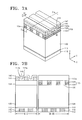
FIG. 1 illustrates a plan view of a semiconductor memory device according to a first embodiment;
FIGS. 2A through 12A illustrate perspective views of stages in a method of forming a capacitor of the semiconductor memory device according to the first embodiment shown in FIG. 1;
FIGS. 2B through 12B illustrate cross-sectional views (taken in directions I-I and II-II) of FIGS. 2A through 12A, respectively;
FIG. 12C illustrates cross-sectional views corresponding to FIG. 12B, and showing a dielectric layer and an upper electrode layer;
FIG. 13 illustrates a perspective view of a semiconductor memory device according to a second embodiment; and
FIG. 14 illustrates a cross-sectional view showing details of a transistor structure of FIG. 13.
DETAILED DESCRIPTION
Korean Patent Application No. 10-2008-0110494, filed on Nov. 7, 2008, in the Korean Intellectual Property Office, and entitled: “Method of Forming Capacitor of Semiconductor Memory Device,” is incorporated by reference herein in its entirety.
Example embodiments will now be described more fully hereinafter with reference to the accompanying drawings; however, they may be embodied in different forms and should not be construed as limited to the embodiments set forth herein. Rather, these embodiments are provided so that this disclosure will be thorough and complete, and will fully convey the scope of the invention to those skilled in the art.
In the drawing figures, the dimensions of layers and regions may be exaggerated for clarity of illustration. It will also be understood that when a layer or element is referred to as being “on” another layer or substrate, it can be directly on the other layer or substrate, or intervening layers may also be present. Further, it will be understood that when a layer is referred to as being “under” another layer, it can be directly under, and one or more intervening layers may also be present. In addition, it will also be understood that when a layer is referred to as being “between” two layers, it can be the only layer between the two layers, or one or more intervening layers may also be present. Like reference numerals refer to like elements throughout.
FIG. 1 illustrates a plan view of a semiconductor memory device according to a first embodiment, and FIG. 12A illustrates a partial perspective view of the semiconductor memory device of FIG. 1.
Referring to FIGS. 1 and 12A, two storage node electrodes 160 may be separately formed on a single storage node contact 112. As shown in FIG. 1, the storage node contacts 112 may be interposed between word lines 103 and bit lines 105. The word lines 103 may extend in a first direction, e.g., parallel to the X-axis, and the bit lines 105 may extend in a second direction, e.g., parallel to the Y-axis.
As shown in FIGS. 1 and 12A, support patterns 131 may be provided between pairs of storage node electrodes 160 in order to support the storage node electrodes 160. As shown in FIG. 1, the support patterns 131 may be formed in the same positions as the bit lines 105. The support patterns 131 may extend parallel to the Y-axis and may be separated from one another, i.e., spaced apart, in the X-axis direction.
FIGS. 2A through 12A illustrate perspective views of stages in a method of forming a capacitor of the semiconductor memory device according to the first embodiment shown in FIG. 1. FIGS. 2B through 12B illustrate cross-sectional views (taken in directions I-I and II-II) of FIGS. 2A through 12A, respectively.
Referring to FIGS. 2A and 2B, an etch stop layer 113 and a mold layer 120 may be sequentially formed on an interlayer dielectric layer 110. The interlayer dielectric layer 110 may have storage node contacts 112 penetrating therethrough and connected to underlying features on a semiconductor substrate (not shown in FIGS. 2A and 2B). For example, a transistor having a gate electrode and source and drain regions may be formed under the interlayer dielectric layer 110. Each of the storage node contacts 112 may be electrically connected to one of the source and drain regions of the transistor, and a bit line may be formed in a direction crossing the gate electrode on the gate electrode of the transistor. The storage node contact 112 may be formed at a same level as the bit line.
The mold layer 120 may provide a mold for forming a pillar-type storage node electrode, as described in further detail below. The mold layer 120 may be formed of silicon oxide such as tetraethoxysilane (TEOS), a high-density plasma (HDP) oxide, phospho-silicate-glass (PSG), undoped-silicate-glass (USG), boro-phospho-silicate-glass (BPSG), spin-on-glass (SOG), etc. The etch stop layer 113 may function to prevent the interlayer dielectric layer 110 disposed under the mold layer 120 from being etched during a subsequent process of etching the mold layer 120. The etch stop layer 113 may be formed of a material, e.g., silicon nitride, having an etch selectivity with respect to the mold layer 120.
Referring to FIGS. 3A and 3B, a support pattern 131 and a support mask pattern 133 may be sequentially formed on the mold layer 120, e.g., by depositing and patterning respective layers using photolithography and etching processes, thereby forming a support structure 130 having the support pattern 131 and the support mask pattern 133. The support pattern 131 may serve to support subsequently-formed storage node electrodes and may prevent the storage node electrodes from collapsing.
The support pattern 131 may be formed of a material, e.g., silicon nitride, having an etch selectivity with respect to the mold layer 120. The support mask pattern 133 may be formed of a material, e.g., polysilicon (poly-Si) or tungsten (W), having an etch selectivity with respect to both the support pattern 131 and the mold layer 120. The support mask pattern 133 may serve as an etch mask and protect the support pattern 131 during a subsequent process of etching the mold layer 120. However, the support mask pattern 133 may be omitted, e.g., if the support pattern 131 itself is used as an etch mask during the etching of the mold layer 120. A buffer layer (not shown) may be formed between the support pattern 131 and the support mask pattern 133. The buffer layer may be, e.g., a silicon oxide layer. The support pattern 131 may have a line shape that extends in the same direction as the bit line. For example, the support pattern 131 may overlap the bit line and extend in the same direction as the bit line.
Referring to FIGS. 4A and 4B, a first sacrificial layer 135 may be formed between the support structures 130, i.e., between the support patterns 131 and the support mask patterns 133. To form the first sacrificial layer 135, gaps between the adjacent support structures 130 may be filled with a layer, e.g., a silicon oxide layer such as an HDP oxide layer, having an etch selectivity with respect to the support pattern 131 and the support mask pattern 133. Then, the silicon oxide layer may be planarized by, e.g., an etchback process or a chemical mechanical polishing (CMP) process, using the support mask pattern 133 as a stop layer, thereby forming the first sacrificial layer 135.
Referring to FIGS. 5A and 5B, a first mask layer 140 may be formed on the support structure 130, i.e., on the support pattern 131 and the support mask pattern 133, and on the first sacrificial layer 135. The first mask layer 140 may be formed of a material having an etch selectivity with respect to the mold layer 120, the first sacrificial layer 135, and the support pattern 131. For example, the first mask layer 140 may be formed of the same material, e.g., poly-Si or W, as the support mask pattern 133.
Referring to FIGS. 6A and 6B, the first mask layer 140 may be patterned to form a first mask pattern 141. The first mask pattern 141 may serve as a first pattern provided in connection with a self-aligned double patterning (SADP) process that is used, along with the support structure 130, to form a storage node electrode hole in the mold layer 120. The first mask pattern 141 may be formed as a line shape in a direction crossing the support structure 130, e.g., crossing at right angles. The first mask pattern 141 may be located between the storage node contacts 112 from the top plan view. For example, the first mask pattern 141 may overlap the word line and may extend in the same direction as the word line. The first mask pattern 141 may be formed by, e.g., depositing a layer and patterning the layer by forming trenches therein.
Referring to FIGS. 7A and 7B, a second sacrificial layer 142 may be formed with a uniform thickness to cover the first mask pattern 141, i.e., the second sacrificial layer 142 may be a conformal layer. For example, the thickness of sidewall portions 142 a of the second sacrificial layer 142 on sidewalls of the first mask pattern 141 and covering a bottom of trenches 143 may be substantially the same. The trenches 143 may be between sidewall portions 142 a of the second sacrificial layer 142, which are formed on opposite sidewalls of adjacent ones of the first mask patterns 141. The second sacrificial layer 142 may be formed of a material layer, e.g., a silicon oxide layer, having an etch selectivity with respect to the first mask pattern 141. To form the second sacrificial layer 142, a silicon oxide layer may be deposited using a conformal deposition process, e.g., a chemical vapor deposition (CVD) process or an atomic layer deposition (ALD) process. The thickness of the second sacrificial layer 142 may determine a first width, in the direction I-I, of a storage node electrode hole formed in a subsequent stage. A second width, in the direction II-II, of the storage node electrode hole may be determined by a distance between the adjacent support patterns 131.
Referring to FIGS. 8A and 8B, a second mask layer may be formed to fill the trenches 143 of the second sacrificial layer 142. The second mask layer and the second sacrificial layer 142 may be planarized, e.g., by an etchback process or a CMP process, until a top surface of the first mask layer 141 is exposed. As a result, a second mask pattern 144 may be formed from the second mask layer in each of the trenches 143. In another implementation, the second mask layer 144 may be formed to fill the trenches 143 of the second sacrificial layer 142 and planarized, e.g., by an etchback process or a CMP process, until a top surface of the second sacrificial layer 142 is exposed. The second mask pattern 144 may be formed in each of the trenches 143. The second sacrificial layer 142 and the second mask pattern 144 may be formed by a self-aligned double patterning (SADP) process using the first mask pattern 141 as a primary pattern.
With the first mask pattern 141 located between the storage node contacts 112 from the top plan view, the sidewall patterns 142 a of the second sacrificial layer 142 and the second mask pattern 144 interposed therebetween may overlap and correspond to the storage node contacts 112 from the top plan view.
Referring to FIGS. 9A and 9B, the second sacrificial layer 142, the first sacrificial layer 135, and the mold layer 120 may be etched, e.g., by an anisotropic etching process, using the first and second mask patterns 141 and 144 as masks, thereby forming storage node electrode holes 152 exposing the storage node contacts 112. The formation of the storage node electrode holes 152 may include removing the sidewall patterns 142 a of the second sacrificial layer 142 interposed between the first and second mask patterns 141 and 144 to form openings 151, and removing the first sacrificial layer 135 and the mold layer 120 disposed under the openings 151 to form the storage node electrode holes 152. In an implementation, the etch stop layer 113 may also be removed.
As described above, in forming the second mask pattern 144, only the second mask layer may be etched, e.g., using the etchback process or the CMP process, until the top surface of the second sacrificial layer 142 is exposed. During the formation of the storage node electrode holes 152 using the anisotropic etching process, removing the second sacrificial layer 142 disposed on the first mask pattern 141 may be followed by removing the exposed sidewall patterns 142 a of the second sacrificial layer 142 interposed between the first and second mask patterns 141 and 144, thereby forming the openings 151. Thereafter, the first sacrificial layer 135 and the mold layer 120 disposed under the openings 151 may be removed using the first and second mask patterns 141 and 144 as masks, thereby forming the storage node electrode holes 152.
The storage node electrode holes 152 may be formed in spaces between the line-shaped support structures 130 (which may be arranged in, i.e., extend in, a first direction I-I) and the line-shaped mask patterns 141 and 144 (which may be arranged in, i.e., extend in, a second direction II-II crossing the first direction I-I). Thus, they maybe separately formed in respective cells. Accordingly, the support structures 130 having the support patterns 131, in combination with the mask patterns 141 and 144, may node-separate the storage node electrode holes 152 in the respective cells. Further, the support mask pattern 133 disposed on the support pattern 131 may function as an etch mask and protect the support pattern 131 during the etching of the mold layer 120.
Referring to FIGS. 10A and 10B, after the storage node electrode holes 152 are formed, the first mask pattern 141, the second mask pattern 144, and the support mask pattern 133 may be removed. If the buffer layer is used between the support pattern 131 and the support mask pattern 133, the buffer layer may also be removed. The first mask pattern 141, the second mask pattern 144, and the support mask pattern 133 may be removed, e.g., by an etchback process or a CMP process, using the support pattern 131 as a stop layer. During the etching process, a portion of the first sacrificial layer 135 remaining between the support mask patterns 133 may also be removed. As a result, top surfaces of the support pattern 131 and the first sacrificial layer 135 formed at the same layer as the support pattern 131 may be exposed.
Referring to FIGS. 11A and 11B, a conductive layer may be formed to fill the storage node electrode holes 152 and then planarized, e.g., by an etchback process or a CMP process, using the support pattern 131 or the first sacrificial layer 135 as a stop layer, to form pillar-type storage node electrodes 160. The conductive layer 160 may be, e.g., a conductive poly-Si layer or a metal layer. For example, the metal layer may be formed of a noble metal such as platinum (Pt), ruthenium (Ru), and iridium (Ir), etc.; a conductive oxide of the noble metal, e.g., RuO2, IrO2, etc.; a refractory metal such as titanium (Ti), tungsten (W), tantalum (Ta), etc.; a conductive nitride of the refractory metal, e.g., TiN, TaN, WN, etc; or combinations of such materials.
Referring to FIGS. 12A and 12B, the first sacrificial layer 135 and the mold layer 120 may be removed, e.g., by anisotropic etching, to leave the storage node electrodes 160 and the support patterns 131. For example, the anisotropic etching process may be performed using an etchant containing water, ammonium fluoride, and fluoric acid. The etchant may selectively remove silicon oxide used to form the first sacrificial layer 135 and the mold layer 120. The etch stop layer 113 remaining under the mold layer 120 may inhibit the etching of the underlying interlayer dielectric layer 110.
After the first sacrificial layer 135 and the mold layer 120 are removed, the pillar-type storage node electrodes 160 may be supported to extend in a vertical direction by the support patterns 131. The support patterns 131 may remain and may extend in a horizontal direction between the storage node electrodes 160. The support patterns 131 may be spaced apart from the interlayer dielectric layer 110, and may have upper surfaces that are substantially co-planar with upper surfaces of the storage node electrodes 160. The pillar-type storage node electrodes 160 having a high aspect ratio, i.e., narrow sectional area and relatively greater height, may be stably supported by the support patterns 131 having a horizontal beam shape, without the storage node electrodes 160 contacting adjacent storage node electrodes 160 and/or falling down.
Subsequently, as shown in FIG. 12C, a dielectric layer 161 and an upper electrode layer 162 may be sequentially formed on the storage node electrodes 160. The upper electrode layer 162 may be electrically connected by contacts to interconnection lines formed on the upper electrode layer 162. The upper electrode layer 162 may be further processed to form respective upper electrodes.
As shown in FIGS. 1 and 12A, two pillar-type storage node electrodes 160 may be in contact with a single storage node contact 112. Thus, two capacitors may be connected in parallel in a single cell. As compared with a case where a single pillar-type storage node electrode is used, the footprint of a capacitor may be increased using the two pillar-type storage node electrodes 160. As a result, the total capacitance of each cell may increase.
As the design rule of a memory device is reduced, a footprint occupied by a capacitor on a substrate may also be reduced. Such reductions in footprint area may make it difficult to fill the typical cylindrical structures with a dielectric material and an upper electrode material. In particular, with a reduction in the design rule, patterns of a cylindrical capacitor may become narrower and higher, i.e., the aspect ratio may increase. As a result, conformally forming a dielectric layer and an upper electrode layer in a cylindrical lower electrode layer becomes progressively more difficult. Further, leakage current may increase, resulting in, e.g., poor data retention in a capacitive storage type memory such as DRAM, and photolithographic limits may hinder patterning of the cylindrical capacitor.
In contrast, the pillar-type storage node electrodes described above may be easier to fill. Furthermore, limitations on exposure limit may be overcome by using the self-aligned double patterning (SADP) process. Accordingly, the storage node electrodes 160 may be separately formed in respective cells using the support patterns 131.
FIG. 13 illustrates a perspective view of a semiconductor memory device in which a capacitor is formed on a semiconductor substrate having an underlying structure with a transistor and a bit line according to an exemplary embodiment. In FIG. 13, a front section is taken in a direction vertical to a lengthwise direction of the bit line. FIG. 14 illustrates a cross-sectional view showing details of a transistor structure of FIG. 13.
Referring to FIG. 13, an active region may be defined by a device isolation layer 201 formed in a semiconductor substrate 200. Source and drain regions 202 may be formed in the active region. As shown in FIG. 14, a gate structure 203 may be disposed to control a channel region between the source and drain regions 202, the source and drain regions 202 and the gate structure 203 forming a transistor 204. In a left section of FIG. 13, although the device isolation layer 201 is illustrated as being parallel to a bit line 221 for brevity, it may have various other shapes according to the type of the active region. A contact pad 213 may be formed in a first interlayer dielectric layer 212 to contact the source and drain regions 202. Although not shown in FIG. 13, word line structures may extend in a direction vertical to the bit line 221 in front of and behind the contact pad 213.
A bit line structure 220 may be formed on a second interlayer dielectric layer 214. The bit line structure 220 may include the bit line 221, a bit line mask layer 222 disposed on the bit line 221, and bit line spacers 223 disposed on sidewalls of the bit line 221 and the bit line mask layer 222. The bit line mask layer 222 and the bit line spacers 223 may protect the bit line 221 during a subsequent process of etching a third interlayer dielectric layer 224 to form storage node contact holes.
A storage node contact 226 may be in contact with the contact pad 213 through the third interlayer dielectric layer 224 and the second interlayer dielectric layer 214. A portion of the contact pad 213, which is not shown in FIG. 13, may be connected to a bit line contact (not shown). A storage node electrode 230 may be formed as a pillar type on the storage node contact 226. A support pattern 232 may extend in the same direction as the bit line 221 between the storage node electrodes 230, and may node-separate and support the storage node electrodes 230. Here, two storage node electrodes 230 may be separately formed on each of the storage node contacts 226.
Example embodiments have been disclosed herein, and although specific terms are employed, they are used and are to be interpreted in a generic and descriptive sense only and not for purpose of limitation. Accordingly, it will be understood by those of ordinary skill in the art that various changes in form and details may be made without departing from the spirit and scope of the present invention as set forth in the following claims.

Claims (11)

1. A method of forming a semiconductor memory device, the method comprising:
forming an interlayer dielectric layer on a semiconductor substrate;
forming storage node contacts that extend through the interlayer dielectric layer;
sequentially forming an etch stop layer and then a mold layer on the interlayer dielectric layer;
forming a plurality of line-shaped support structures and a first sacrificial layer filling gaps between the support structures on the mold layer, the support structures extending in a first direction;
sequentially forming a plurality of line-shaped first mask patterns, a second sacrificial layer, and then second mask patterns on the support structures and on the first sacrificial layer, the first mask patterns extending in a second direction crossing the first direction, the second sacrificial layer covering the first mask patterns to a uniform thickness, and the second mask patterns being formed in trenches in the second sacrificial layer between adjacent ones of the first mask patterns;
removing the second sacrificial layer, the first sacrificial layer, and the mold layer using the first mask patterns, the second mask patterns, and the support structures as masks to form storage node electrode holes that expose surfaces of the storage node contacts;
removing the first mask patterns and second mask patterns to expose the support structures;
filling the storage node electrode holes with a conductive material and etching back the conductive material to expose the support structures; and
removing the first sacrificial layer and the mold layer to form pillar-type storage node electrodes supported by the support structures.
2. The method as claimed in claim 1, wherein:
a portion of the second sacrificial layer covers facing sidewalls of adjacent first mask patterns, and
removing the second sacrificial layer, the first sacrificial layer, and the mold layer forms two storage node electrode holes that both expose a surface of a same storage node contact.
3. The method as claimed in claim 1, wherein:
each of the support structures includes a support pattern and a support mask pattern disposed on the support pattern, and
removing the first and second mask patterns to expose the support structures includes removing the support mask pattern to expose the support pattern.
4. The method as claimed in claim 3, wherein:
the first mask pattern is formed of a material having an etch selectivity with respect to each of the support pattern, the first sacrificial layer, the second sacrificial layer, and the mold layer, and
the second mask pattern is formed of a material having an etch selectivity with respect to each of the support pattern, the first sacrificial layer, the second sacrificial layer, and the mold layer.
5. The method as claimed in claim 1, wherein the support pattern is formed of a material having an etch selectivity with respect to each of the first sacrificial layer, the second sacrificial layer, and the mold layer.
6. The method as claimed in claim 1, wherein forming the second mask patterns includes:
forming a second mask layer on the semiconductor substrate, the second mask layer filling the trenches in the second sacrificial layer; and
removing the second mask layer and the second sacrificial layer until the first mask layer is exposed.
7. The method as claimed in claim 1, wherein forming the second mask patterns includes:
forming a second mask layer on the semiconductor substrate, the second mask layer filling the trenches in the second sacrificial layer; and
removing the second mask layer until the second sacrificial layer is exposed.
8. The method as claimed in claim 1, further comprising forming a transistor under the interlayer dielectric layer, the transistor having a gate electrode, a source region, and a drain region, wherein:
the storage node contact is formed to be electrically connected to one of the source region and the drain region of the transistor.
9. The method as claimed in claim 1, further comprising forming a bit line under the interlayer dielectric layer and extending parallel to the support structures.
10. The method as claimed in claim 1, further comprising sequentially forming a dielectric layer and then an upper electrode layer on the conductive material that fills the storage node electrode holes.
11. A method of forming a memory device, the method comprising:
forming a transistor on a semiconductor substrate, the transistor including a source/drain region electrically coupled to an overlying storage structure via a contact;
forming a first temporary layer covering the transistor;
forming first and second patterns at a same level on the first temporary layer, the first and second patterns being spaced apart from one another on the first temporary layer;
forming third and fourth patterns at a same level on the first and second patterns, the third and fourth patterns being spaced apart from one another and defining, in combination with the first and second patterns, an enclosed area above the contact;
forming a fifth pattern that divides the enclosed area into two portions;
forming a pair of storage node electrode holes in the divided enclosed area using an etch operation, the first through fifth patterns serving as etch masks during the etch operation;
forming storage node electrodes in the pair storage node electrode holes, such that each storage node electrode is electrically connected to a same source/drain region of the transistor via the contact; and
removing the temporary layer and the third, fourth, and fifth patterns so as to leave the first and second patterns in contact with upper portions of the storage node electrodes, the first and second patterns reinforcing the upper portions of the storage node electrodes.
US12/591,072 2008-11-07 2009-11-06 Method of forming capacitor of semiconductor memory device Active 2029-12-03 US8043925B2 (en)

Applications Claiming Priority (2)

Application Number Priority Date Filing Date Title
KR1020080110494A KR101469098B1 (en) 2008-11-07 2008-11-07 Method for formation of capacitor of semiconductor memory device
KR10-2008-0110494 2008-11-07

Publications (2)

Publication Number Publication Date
US20100120212A1 US20100120212A1 (en) 2010-05-13
US8043925B2 true US8043925B2 (en) 2011-10-25

Family

ID=42165586

Family Applications (1)

Application Number Title Priority Date Filing Date
US12/591,072 Active 2029-12-03 US8043925B2 (en) 2008-11-07 2009-11-06 Method of forming capacitor of semiconductor memory device

Country Status (2)

Country Link
US (1) US8043925B2 (en)
KR (1) KR101469098B1 (en)

Cited By (5)

* Cited by examiner, † Cited by third party
Publication number Priority date Publication date Assignee Title
US20100187101A1 (en) * 2009-01-23 2010-07-29 Samsung Electronics Co., Ltd. Method of manufacturing the semiconductor device
US20150193570A1 (en) * 2014-01-09 2015-07-09 Moon-gyu JEONG Methods of Patterning Wafers Using Self-Aligned Double Patterning Processes
US20160104642A1 (en) * 2013-12-18 2016-04-14 Robert L. Bristol Self-aligned via and plug patterning with photobuckets for back end of line (beol) interconnects
US9871093B2 (en) 2016-02-17 2018-01-16 Samsung Electonics Co., Ltd. Semiconductor devices
US10276668B2 (en) 2016-12-08 2019-04-30 Samsung Electronics Co., Ltd. Lower cylinderical electrodes forming a honey comb structure with plurality support structures

Families Citing this family (8)

* Cited by examiner, † Cited by third party
Publication number Priority date Publication date Assignee Title
JP2009141073A (en) * 2007-12-05 2009-06-25 Elpida Memory Inc Method of manufacturing semiconductor device, and semiconductor device
KR101658492B1 (en) * 2010-08-13 2016-09-21 삼성전자주식회사 Method for forming fine patterns and method for manufacturing a semiconductor device by using the same
US9583435B2 (en) * 2013-03-15 2017-02-28 Microchip Technology Incorporated Forming fence conductors using spacer etched trenches
KR102295966B1 (en) * 2014-08-27 2021-09-01 삼성전자주식회사 Method of Fabricating Semiconductor Devices Using Nanowires
DE102016114724B4 (en) 2016-03-25 2021-08-12 Taiwan Semiconductor Manufacturing Company, Ltd. Method of forming trenches of different depths and apparatus - US Pat
US9779984B1 (en) 2016-03-25 2017-10-03 Taiwan Semiconductor Manufacturing Co., Ltd. Method of forming trenches with different depths
US10395978B2 (en) * 2017-02-27 2019-08-27 Imec Vzw Method of patterning target layer
CN111403343B (en) * 2019-01-02 2022-08-30 联华电子股份有限公司 Method for forming semiconductor pattern

Citations (7)

* Cited by examiner, † Cited by third party
Publication number Priority date Publication date Assignee Title
KR20030019639A (en) 2000-07-31 2003-03-06 인피네온 테크놀로지스 아게 Semiconductor memory cell arrangement and method for producing the same
KR20040001274A (en) 2002-06-27 2004-01-07 삼성전자주식회사 Semiconductor memory device and method for manufacturing the same
KR20040008698A (en) 2002-07-19 2004-01-31 주식회사 하이닉스반도체 Method for fabricating capacitor in semiconductor device
US20040115884A1 (en) 2002-08-02 2004-06-17 Ting-Shing Wang [dynamic random access memory cell and fabrication thereof]
US6914286B2 (en) * 2002-06-27 2005-07-05 Samsung Electronics Co., Ltd. Semiconductor memory devices using sidewall spacers
US20100200901A1 (en) * 2009-02-12 2010-08-12 Kim Gil-Sub Semiconductor memory device having cylinder-type capacitor lower electrode and associated methods
US7897474B2 (en) * 2007-12-05 2011-03-01 Elpida Memory, Inc. Method of forming semiconductor device including capacitor and semiconductor device including capacitor

Family Cites Families (3)

* Cited by examiner, † Cited by third party
Publication number Priority date Publication date Assignee Title
KR100334577B1 (en) * 1999-08-06 2002-05-03 윤종용 Method of forming a trench in an insulating layer exceeding the photolithographic resolution in a semiconductor manufacturing
KR100549012B1 (en) * 2004-06-24 2006-02-02 삼성전자주식회사 semiconductor device having cylinder storage nodes of box type and fabrication method thereof
KR20070122050A (en) * 2006-06-23 2007-12-28 주식회사 하이닉스반도체 Pattern forming method using double patterning process

Patent Citations (8)

* Cited by examiner, † Cited by third party
Publication number Priority date Publication date Assignee Title
KR20030019639A (en) 2000-07-31 2003-03-06 인피네온 테크놀로지스 아게 Semiconductor memory cell arrangement and method for producing the same
US6853023B2 (en) 2000-07-31 2005-02-08 Infineon Technologies Ag Semiconductor memory cell configuration and a method for producing the configuration
KR20040001274A (en) 2002-06-27 2004-01-07 삼성전자주식회사 Semiconductor memory device and method for manufacturing the same
US6914286B2 (en) * 2002-06-27 2005-07-05 Samsung Electronics Co., Ltd. Semiconductor memory devices using sidewall spacers
KR20040008698A (en) 2002-07-19 2004-01-31 주식회사 하이닉스반도체 Method for fabricating capacitor in semiconductor device
US20040115884A1 (en) 2002-08-02 2004-06-17 Ting-Shing Wang [dynamic random access memory cell and fabrication thereof]
US7897474B2 (en) * 2007-12-05 2011-03-01 Elpida Memory, Inc. Method of forming semiconductor device including capacitor and semiconductor device including capacitor
US20100200901A1 (en) * 2009-02-12 2010-08-12 Kim Gil-Sub Semiconductor memory device having cylinder-type capacitor lower electrode and associated methods

Cited By (7)

* Cited by examiner, † Cited by third party
Publication number Priority date Publication date Assignee Title
US20100187101A1 (en) * 2009-01-23 2010-07-29 Samsung Electronics Co., Ltd. Method of manufacturing the semiconductor device
US20160104642A1 (en) * 2013-12-18 2016-04-14 Robert L. Bristol Self-aligned via and plug patterning with photobuckets for back end of line (beol) interconnects
US9553018B2 (en) * 2013-12-18 2017-01-24 Intel Corporation Self-aligned via and plug patterning with photobuckets for back end of line (BEOL) interconnects
US20150193570A1 (en) * 2014-01-09 2015-07-09 Moon-gyu JEONG Methods of Patterning Wafers Using Self-Aligned Double Patterning Processes
US9311439B2 (en) * 2014-01-09 2016-04-12 Samsung Electronics Co., Ltd. Methods of patterning wafers using self-aligned double patterning processes
US9871093B2 (en) 2016-02-17 2018-01-16 Samsung Electonics Co., Ltd. Semiconductor devices
US10276668B2 (en) 2016-12-08 2019-04-30 Samsung Electronics Co., Ltd. Lower cylinderical electrodes forming a honey comb structure with plurality support structures

Also Published As

Publication number Publication date
US20100120212A1 (en) 2010-05-13
KR101469098B1 (en) 2014-12-04
KR20100051361A (en) 2010-05-17

Similar Documents

Publication Publication Date Title
US8043925B2 (en) Method of forming capacitor of semiconductor memory device
US7670903B2 (en) Method for fabricating a cylindrical capacitor using amorphous carbon-based layer
US8395235B2 (en) Semiconductor device
TWI762156B (en) Semiconductor memory device and method of fabricating same
US20070281461A1 (en) Semiconductor device having a contact structure with a contact spacer and method of fabricating the same
KR20170087803A (en) Semiconductor memory device having enlarged cell contact area and method of fabricating the same
CN101335242B (en) Method for fabricating semiconductor device
US8822302B2 (en) Methods of fabricating a storage node in a semiconductor device and methods of fabricating a capacitor using the same
US20120217576A1 (en) Semiconductor device and method for forming the same
JP2008113005A (en) Method of manufacturing integrated semiconductor structure
US9252046B2 (en) Semiconductor device and method for manufacturing the same
JP2010034198A (en) Semiconductor device and method of manufacturing the same
US6992346B2 (en) Integrated circuit devices with metal-insulator-metal capacitors
US20120205810A1 (en) Semiconductor device and fabricating method thereof
US11152368B2 (en) Semiconductor device including storage node electrode having filler and method for manufacturing the same
US11355497B2 (en) Memory cell capacitor with varying width and supportive structures
US9362421B2 (en) Semiconductor device including a support structure
KR20090099775A (en) Method for manufacturing capacitor with pillar type storagenode
US7964501B2 (en) Semiconductor device and method of fabricating the same
KR20090068776A (en) Capacitor in semiconductor device and method for manufacturing the same
KR20190062028A (en) Semiconductor storage device
KR20230018830A (en) Semiconductor devices having supporter structures
US11393823B2 (en) Semiconductor device and manufacturing method of semiconductor device
CN113130495B (en) Semiconductor device and method of forming the same
JP2002110945A (en) Semiconductor device and its manufacturing method

Legal Events

Date Code Title Description
AS Assignment

Owner name: SAMSUNG ELECTRONICS CO., LTD.,KOREA, REPUBLIC OF

Free format text: ASSIGNMENT OF ASSIGNORS INTEREST;ASSIGNORS:YANG, DONG-KWAN;KIM, SEONG-HO;PARK, WON-MO;AND OTHERS;REEL/FRAME:023531/0806

Effective date: 20091106

Owner name: SAMSUNG ELECTRONICS CO., LTD., KOREA, REPUBLIC OF

Free format text: ASSIGNMENT OF ASSIGNORS INTEREST;ASSIGNORS:YANG, DONG-KWAN;KIM, SEONG-HO;PARK, WON-MO;AND OTHERS;REEL/FRAME:023531/0806

Effective date: 20091106

STCF Information on status: patent grant

Free format text: PATENTED CASE

FPAY Fee payment

Year of fee payment: 4

MAFP Maintenance fee payment

Free format text: PAYMENT OF MAINTENANCE FEE, 8TH YEAR, LARGE ENTITY (ORIGINAL EVENT CODE: M1552); ENTITY STATUS OF PATENT OWNER: LARGE ENTITY

Year of fee payment: 8

MAFP Maintenance fee payment

Free format text: PAYMENT OF MAINTENANCE FEE, 12TH YEAR, LARGE ENTITY (ORIGINAL EVENT CODE: M1553); ENTITY STATUS OF PATENT OWNER: LARGE ENTITY

Year of fee payment: 12