US8043427B2 - Semiconductor wafers of silicon and method for their production - Google Patents
Semiconductor wafers of silicon and method for their production Download PDFInfo
- Publication number
- US8043427B2 US8043427B2 US12/011,713 US1171308A US8043427B2 US 8043427 B2 US8043427 B2 US 8043427B2 US 1171308 A US1171308 A US 1171308A US 8043427 B2 US8043427 B2 US 8043427B2
- Authority
- US
- United States
- Prior art keywords
- single crystal
- phase boundary
- melt
- rmax
- ratio
- Prior art date
- Legal status (The legal status is an assumption and is not a legal conclusion. Google has not performed a legal analysis and makes no representation as to the accuracy of the status listed.)
- Active, expires
Links
Images


Classifications
-
- C—CHEMISTRY; METALLURGY
- C30—CRYSTAL GROWTH
- C30B—SINGLE-CRYSTAL GROWTH; UNIDIRECTIONAL SOLIDIFICATION OF EUTECTIC MATERIAL OR UNIDIRECTIONAL DEMIXING OF EUTECTOID MATERIAL; REFINING BY ZONE-MELTING OF MATERIAL; PRODUCTION OF A HOMOGENEOUS POLYCRYSTALLINE MATERIAL WITH DEFINED STRUCTURE; SINGLE CRYSTALS OR HOMOGENEOUS POLYCRYSTALLINE MATERIAL WITH DEFINED STRUCTURE; AFTER-TREATMENT OF SINGLE CRYSTALS OR A HOMOGENEOUS POLYCRYSTALLINE MATERIAL WITH DEFINED STRUCTURE; APPARATUS THEREFOR
- C30B29/00—Single crystals or homogeneous polycrystalline material with defined structure characterised by the material or by their shape
- C30B29/02—Elements
- C30B29/06—Silicon
-
- H—ELECTRICITY
- H10—SEMICONDUCTOR DEVICES; ELECTRIC SOLID-STATE DEVICES NOT OTHERWISE PROVIDED FOR
- H10P—GENERIC PROCESSES OR APPARATUS FOR THE MANUFACTURE OR TREATMENT OF DEVICES COVERED BY CLASS H10
- H10P14/00—Formation of materials, e.g. in the shape of layers or pillars
- H10P14/20—Formation of materials, e.g. in the shape of layers or pillars of semiconductor materials
-
- C—CHEMISTRY; METALLURGY
- C30—CRYSTAL GROWTH
- C30B—SINGLE-CRYSTAL GROWTH; UNIDIRECTIONAL SOLIDIFICATION OF EUTECTIC MATERIAL OR UNIDIRECTIONAL DEMIXING OF EUTECTOID MATERIAL; REFINING BY ZONE-MELTING OF MATERIAL; PRODUCTION OF A HOMOGENEOUS POLYCRYSTALLINE MATERIAL WITH DEFINED STRUCTURE; SINGLE CRYSTALS OR HOMOGENEOUS POLYCRYSTALLINE MATERIAL WITH DEFINED STRUCTURE; AFTER-TREATMENT OF SINGLE CRYSTALS OR A HOMOGENEOUS POLYCRYSTALLINE MATERIAL WITH DEFINED STRUCTURE; APPARATUS THEREFOR
- C30B15/00—Single-crystal growth by pulling from a melt, e.g. Czochralski method
- C30B15/20—Controlling or regulating
- C30B15/203—Controlling or regulating the relationship of pull rate (v) to axial thermal gradient (G)
Definitions
- the invention relates to a method for producing semiconductor wafers of silicon, comprising pulling a single crystal growing on a phase boundary from a melt contained in a crucible and cutting semiconductor wafers from the pulled single crystal, wherein heat is delivered to a center of the phase boundary during pulling, and a radial profile of a ratio V/G from the center to an edge of the phase boundary is controlled, with G being the temperature gradient perpendicular to the phase boundary and V being the pull rate at which the single crystal is pulled from the melt.
- the invention also relates to defect-free semiconductor wafers of silicon, which can be produced by this method.
- Semiconductor wafers of silicon in the context of the invention are referred to as defect-free so long as neither OSF defects, A-swirl defects, nor COP defects with a size of more than 30 nm are detectable.
- a method in the context of this invention is regarded as economically viable when, in particular, it is possible to pull single crystals with a diameter of at least 300 mm from a crucible at a rate which is equal to at least 0.5 mm/min and defect-free semiconductor wafers are produced in a high yield, expressed in terms of the total yield of semiconductor wafers.
- vacancies form vacancy agglomerates (voids) which, depending on the detection method, are referred to inter alia as COP defects (crystal originated particles, COPs), FPD (flow pattern defects), LLS (localized light scatterers) or DSOD (direct surface oxide defects).
- COP defects crystal originated particles, COPs
- FPD flow pattern defects
- LLS localized light scatterers
- DSOD direct surface oxide defects
- the intrinsic point defect type which is incorporated in excess into the crystal lattice when pulling the single crystal depends essentially on the ratio of the pull rate V, at which the single crystal is pulled from the melt, and the temperature gradient G perpendicular to the phase boundary between the growing single crystal and the melt.
- V pull rate
- G temperature gradient
- the axial temperature gradient directed perpendicularly to the surface of the melt is also used in model calculations. If the ratio V/G falls below a critical ratio, then an excess of silicon interstitials is created. If the critical ratio is exceeded, then vacancies predominate.
- the size of the COP defects formed depends essentially on two process parameters, namely the aforementioned ratio V/G and the rate at which the single crystal is cooled in the range of from approximately 1100° C. to 1000° C., the nucleation temperature of voids.
- the COP defects are therefore commensurately smaller as the ratio V/G lies closer to the critical ratio and the more rapidly the single crystal is cooled in this temperature range.
- attempts are therefore made to control the two process parameters when pulling the single crystal, so that the defects created by supersaturation of vacancies remain small enough not to interfere with the production of electronic components. Since the structure widths of the components decrease with each generation, the defect size which can still be tolerated decreases accordingly.
- the oxygen forms small so-called precipitates in the single crystal (as grown bulk micro defects, BMDs). These are desirable to a certain extent because they can bind (getter) metallic impurities to themselves, and thus can be used in order to move such contaminants away from the region of the surface into the interior (bulk) of the semiconductor wafer.
- OSF zone oxidation induced stacking faults
- the presence of a zone with such nuclei is usually detected by subjecting a semiconductor wafer, cut from the single crystal, to oxidation in wet oxygen at about 1100° C. for a few hours so that OSF defects are formed. Since this defect type is likewise detrimental to the functional integrity of electronic components, endeavors are made to suppress OSF formation, for example by reducing the concentration of oxygen in the melt so that less oxygen is incorporated into the single crystal than would be necessary in order to form OSF defects.
- the OSF zone can also be avoided by modifying the ratio V/G, for example by using higher or lower pull rates.
- the formation of OSF nuclei can moreover be reduced by higher cooling rates (in the temperature range of precipitation around 900° C.). It is furthermore known that in order to avoid OSF defects, it is advantageous for the single crystal to contain a small concentration of hydrogen.
- U.S. Pat. No. 6,869,478 B2 discloses that a phase boundary curved in the direction of the single crystal generates a temperature gradient which is steepest perpendicular to the phase boundary. Taking into account the Voronkov model, according to which point defects diffuse in the direction of the temperature gradient and according to which silicon interstitials diffuse faster than vacancies, it is furthermore disclosed that the radial diffusion of silicon interstitials due to the curvature of the phase boundary increases the concentration of vacancies at the center of the phase boundary. The ratio V/G, at which the concentrations of vacancies and silicon interstitials correspond to each other, will therefore be commensurately less as the phase boundary is curved more strongly toward the single crystal.
- the present inventors found that the predictions for defect distributions, even when they take the radial distribution into account, differ commensurately more strongly from the defect distributions found in experiments as the rate at which the single crystal is pulled is faster, and as the diameter of the single crystal is greater.
- FIG. 1 shows an extreme example of this observation.
- a single crystal of silicon with a nominal diameter of 300 mm was pulled at a high pull rate and an inhomogeneous radial profile of V/G was adjusted.
- V/G was adjusted to be so low that the formation of A-swirl defects could be expected in this region according to the predictions of the Voronkov model.
- COP defects with a diameter of more than 30 nm were found.
- the ratio V/G was adjusted to be so high that large COP defects should be formed there. In fact, however, A-swirl defects were found.
- FIG. 1 illustrates defect inconsistencies occurring in actual growth of large single crystal silicon in contradiction to predicted defect patterns with adjustment of V/G ratio radial profile to near the critical ratio.
- FIG. 2 illustrates the relationship of V/G and the magnitude of thermomechanical stress.
- FIG. 3 illustrates the relationship between V/G in the region of compressive stress and in the region of tensile stress and the importance of maintaining the radial profile of V/G such that (V/G) t /(V/G) c is greater than 1.5.
- FIG. 4 illustrates the differences between one embodiment of a subject invention wafer and prior art wafers with respect to attitude angle.
- FIG. 5 illustrates a preferred axial temperature profile in accordance with one embodiment of the present invention.
- FIGS. 6 a and 6 b respectively illustrate the relationship between the radial profile of the temperature gradient G an the magnitude of the thermomechanical stress fields for a ( 6 a ) homogenous radial profile V/G, and in inhomogeneous radial profile ( 6 b ) in accordance with one embodiment of the present invention.
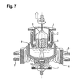
- FIG. 7 illustrates one crystal growth device suitable for use in the method of the present invention.
- FIG. 8 illustrates thermomechanical stress zones in the hot zone of a growing crystal.
- FIGS. 9 a and 9 b illustrate the attitude angle ⁇ as revealed by photoscan of a longitudinal section of a pulled single crystal and a wafer, respectively.
- the invention thus relates to a method for producing semiconductor wafers of silicon, comprising pulling a single crystal growing on a phase boundary from a melt contained in a crucible and cutting of semiconductor wafers from the pulled single crystal, wherein heat is delivered to a center of the phase boundary during pulling, and a radial profile of a ratio V/G from the center to an edge of the phase boundary is controlled, with G being the temperature gradient perpendicular to the phase boundary and with V being the pull rate at which the single crystal is pulled from the melt, wherein the radial profile of the ratio V/G is controlled so that the effect of thermomechanical stress fields in the single crystal adjoining the phase boundary is compensated for with respect to the creation of intrinsic point defects.
- thermomechanical stress fields As a possible cause by which experimental observations may be explained plausibly.
- Thermomechanical stress fields can influence the concentration of intrinsic point defects, and therefore indirectly also defect formation, in a surprisingly strong way.
- the strength of the thermomechanical stress fields must be reduced and their effect must be compensated for in the configuration of the radial profile of V/G, so that in particular single crystals with a diameter of at least 300 mm, from which defect-free semiconductor wafers can be produced, can be pulled economically.
- thermomechanical stress fields in crystallizing silicon have addressed thermomechanical stress fields in crystallizing silicon and their effect on the diffusivity and solubility of intrinsic point defects. Although they come to the conclusion that the formation of silicon interstitials is thermodynamically promoted in the region of tensile stress and the formation of vacancies in the region of compressive stress, their model calculations also show that this should not exert any special effects on defect formation.
- thermomechanical stress fields can be considerable, and that the magnitude of the stress fields must be limited. Furthermore, their effect must be compensated for with respect to the creation of intrinsic point defects.
- This is expediently done by keeping the temperature gradient G, in a region of the single crystal which is under compressive stress and adjoins a central zone of the phase boundary, greater than in a region which is under tensile stress, adjoins an edge region of the single crystal and extends as far as the phase boundary.
- the greater temperature gradient in the region of the compressive stresses makes a larger number of silicon interstitials available, which eliminate the vacancies also present owing to the compressive stresses.
- a maximally homogeneous radial profile of V/G is not desirable, but instead an inhomogeneous radial profile with a V/G at the phase boundary in the region of the compressive stresses which is less than the critical ratio, and with a V/G at the phase boundary in the region of the tensile stresses which is greater than the critical ratio is desired.
- the critical ratio is the ratio V/G which is a prerequisite in the case of a flat phase boundary according to the Voronkov model, so that a defect-forming excess of point defects is not created.
- FIG. 2 shows that the ratio V/G in the regions of the thermomechanical stress fields must differ ever more strongly from the critical ratio as the strength of the thermomechanical stress fields increases.
- the compressive and tensile stresses to be expected can be predicted by simulation calculations. Commercially available programs may be used for the calculation, for example the Flow Module program from Semiconductor Technology Research, Inc.
- FIG. 3 shows in particular that it is the ratio between V/G in the region of the compressive stresses and V/G in the region of the tensile stresses which is important.
- the radial profile of V/G is preferably controlled so that (V/G)t/(V/G)c is at least greater than 1.5, preferably greater than 1.8 and more preferably greater than 2, where (V/G)c is the lowest ratio V/G in the region which is under compressive stress and (V/G)t is the highest ratio V/G in the region which is under tensile stress.
- a strategy based exclusively on the Voronkov model such as the one formulated for example in DE 103 39 792 A1, attempts to provide a radial profile of V/G which is homogeneous and which differs as little as possible from the critical ratio.
- the present invention overcomes this shortcoming since the inventive method makes it possible to obtain defect-free semiconductor wafers of silicon from single crystals having a diameter of at least 300 mm, and which are pulled economically at rates of at least 0.5 mm/min.
- Such semiconductor wafers which are also suitable as substrates for producing epitaxial semiconductor wafers and SOI wafers, can also be readily distinguished from defect-free semiconductor wafers of silicon which come from single crystals pulled in the known way, and specifically by the radial profile of the attitude angle ⁇ of oxygen and dopant striations.
- the Voronkov model predicts that single crystals for defect-free semiconductor wafers can be pulled rapidly only if the temperature gradient G is increased. Only in this way can the pull rate V be increased and the critical ratio V/G maintained at the same time.
- the increased heat supply means that the phase boundary assumes the shape of a surface curved convexly toward the single crystal.
- the extent of the curvature can be specified by a height h.
- the phase boundary may also be regarded as an isothermal surface, i.e. as a surface which is formed by points at which the same temperature prevails.
- the concentration at which oxygen and dopants, for example boron, phosphorus, arsenic or antimony, are absorbed into the single crystal is sensitive to the temperature in the region of the phase boundary. Inevitable temperature variations not only lead to the axial position of the phase boundary varying by small amounts over the course of time, but also to a take-up of oxygen and dopants into the single crystal which varies as a function of time.
- the different concentrations of these elements can be revealed in the form of growth striations, which are formed according to the profile of the phase boundary.
- the growth striations appear as rings, and as curved lines in side view of a cross section through the semiconductor wafer or through a longitudinal section through a piece of the single crystal.
- the profile of the attitude angle ⁇ of these lines provides information regarding the curvature of the phase boundary when pulling the single crystal. Since single crystals with such a profile of attitude angle can only be produced by the method according to the invention, in so far as they deliver defect-free semiconductor wafers of silicon, the profile of the attitude angle ⁇ is an unequivocal indicator for the application of the method according to the invention.
- FIG. 4 graphically represents the way in which semiconductor wafers according to the invention can differ from those of the prior art. If the attitude angle ⁇ is plotted against the radius of the semiconductor wafer, then it is only for semiconductor wafers according to the invention that the resulting line lies in a zone that is described by the specified inequality. The zone is restricted to radial positions r/rmax of from 0.1 to 0.9, because the attitude angle ⁇ in the adjoining regions can not be determined accurately.
- FIG. 4 also indicates the profile of the attitude angle ⁇ obtained for semiconductor wafers which are produced according to the methods described in U.S. Pat. No. 6,869,478 B2 and DE 103 39 792 A1, respectively.
- the semiconductor wafers according to the invention preferably also contain at least one of the elements carbon, nitrogen and hydrogen. If nitrogen is present, then the concentration is preferably from 2.0 ⁇ 10 13 to 1.0 ⁇ 10 15 atoms/cm 3 .
- the presence of carbon, nitrogen or both elements assists the formation of BMDs and therefore improves getterability. It is thus particularly advantageous for the oxygen concentration to be comparatively low when these dopants are present.
- the presence of hydrogen hinders the formation of OSF defects, and thus makes it particularly advantageous for the oxygen concentration to be comparatively high.
- any measure may be envisaged which is known to have an effect on one of these parameters. Since there is little latitude for varying the pull rate owing to the criterion of having to be able to pull as economically as possible and therefore as rapidly as possible, most of these measures are aimed at adjusting the radial profile of the temperature gradient G, particularly in the regions of the compressive and tensile stresses, according to the specifications of the invention. This is best achieved by suitably configuring and influencing the close vicinity of the single crystal, the so-called hot zone, and, accordingly, also by suitable measures for supplying heat to the single crystal and dissipating heat from the single crystal.
- An example particularly to be mentioned is the use of a heat source, by which heat can be transported in a particular degree to the center of the phase boundary, and particularly in the configuration of a heater which is arranged below the crucible center and can be raised and lowered with the crucible.
- a heater is particularly preferred when it generates a radial temperature profile at the crucible bottom, with a pronounced temperature maximum at the center of the crucible bottom.
- the crucible bottom may be heated with the aid of a heat source which is arranged statically under the crucible and is therefore not raised together with the crucible when pulling the single crystal.
- heat is thus preferably delivered to the melt in three ways.
- the desired heat transport directed toward the center of the phase boundary may also be brought about by rotating the crucible and the single crystal in the same sense, even though the increase of G thereby achieved is less pronounced.
- magnetic fields in particular horizontal fields or CUSP fields or traveling magnetic fields, not only can the concentration of oxygen in the single crystal be limited, but also an effect can be exerted on the heat transport.
- CUSP fields in particular are suitable as means for focusing a melt flow which is directed upward toward the center of the phase boundary and transports heat.
- a further instrument for increasing the temperature gradient G is a cooler, which surrounds the single crystal and effectively dissipates heat from the single crystal.
- a heat source which heats an edge of the single crystal adjoining the phase boundary, most preferably in the configuration of an annular heater surrounding the single crystal near the surface of the melt.
- the annular heater and the cooler are preferably operated in such a way that the axial temperature profile on the surface of the single crystal can be described by a curve which has at least one point of inflexion, i.e. can be approximated by a polynomial of at least third order, and which therefore differs from the parabolic temperature profile described in U.S. Pat. No. 6,869,478 B2.
- the preferred axial temperature profile is represented in FIG. 5 .
- the single crystal is preferably not cooled until a distance above the surface of the melt which is greater than the height h between the center of the phase boundary and the surface of the melt.
- FIGS. 6 a and 6 b show a comparison of the radial profile of the temperature gradient G and the strength of the thermomechanical stress fields, when, for the rapid pulling of large single crystals, on the one hand the strategy is adopted of keeping the radial profile of V/G as homogeneous as possible and close to the critical ratio ( FIG. 6 a ), and on the other hand proceeding according to the invention ( FIG. 6 b ). If the radial profile of V/G is configured homogeneously, then a region is formed in the single crystal with strongly pronounced compressive stresses, which adjoins a central zone of the phase boundary, and a region with strongly pronounced tensile stresses which adjoins an edge region of the single crystal and the phase boundary.
- the height h is preferably at least 20 mm.
- the oxygen concentration in the single crystal is also preferably controlled, so that no OSF defects are formed even if the single crystal is pulled under conditions which promote the formation of such defects.
- a concentration according to ASTM Standard F121-83 in the range of from 5 ⁇ 10 17 atoms/cm 3 to 6.5 ⁇ 10 17 atoms/cm 3 is preferably adjusted.
- the oxygen concentration is preferably controlled via the field strength generated by the magnet coils, via the pressure in the pulling system and via the flow rate per unit time with which an inert gas, for example argon, is fed through the pulling system, or by a combination of these control instruments.
- the oxygen content in the single crystal is dependent on the melt flows.
- Field strengths of at least 10 mT (7960 A/m) to 80 mT (63700 A/m) in the melt are particularly preferred in the region of the pulling axis, as well as a pressure-flow rate ratio of from 0.004 to 0.03 mbar/(1/h).
- the device represented in FIG. 7 comprised a crucible 8 containing the melt and a side heater 6 surrounding the crucible, as well as a heat shield 2 .
- the device furthermore contained two mutually opposite magnetic field coils 5 which generated a CUSP magnetic field, and a bottom heater 10 raisable with the crucible for transporting heat to the center of the phase boundary of the growing single crystal 9 .
- Other features of the pulling device were a stationary bottom heater 7 , a cooler 1 surrounding the single crystal and cooled with water and blackened on the inner surface, as well as an annular heater 3 .
- thermomechanical stress fields in the single crystal was compiled for this hot zone with the aid of simulation calculations.
- the aforementioned Flow Module program which two-dimensionally calculates the elastic stresses axisymmetrically and isotropically, was used as the simulation program.
- thermomechanical stresses of up to ⁇ 26 MPa were found in the region of the compressive stresses, and up to 7.53 MPa in the region of the tensile stresses.
- the radial profile of V/G was modified and adjusted according to the representation in FIG.
- FIGS. 9 a and 9 b show the result of a photoscan, by which the profile of the dopant striations was revealed.
- charge carriers are stimulated by laser light and detected electrically.
- FIG. 9 a shows the side view of a panel-shaped longitudinal section through an 80 mm long piece of the pulled single crystal.
- FIG. 9 b represents the way in which the radial profile of the attitude angle ⁇ is established by evaluating the side view of a cross section through the semiconductor wafer.
- the radial profile established for the attitude angle ⁇ in the example corresponded to the profile represented in FIG. 4 .
- the radial profile of the attitude angle ⁇ may also be established by a similar evaluation of oxygen striations.
- the oxygen striations are revealed by etching the fracture edge after the precipitation of oxygen by a heat treatment, and assessing it by oblique exposure to UV light.
Landscapes
- Chemical & Material Sciences (AREA)
- Engineering & Computer Science (AREA)
- Crystallography & Structural Chemistry (AREA)
- Materials Engineering (AREA)
- Metallurgy (AREA)
- Organic Chemistry (AREA)
- Crystals, And After-Treatments Of Crystals (AREA)
Abstract
Description
Claims (14)
Priority Applications (2)
| Application Number | Priority Date | Filing Date | Title |
|---|---|---|---|
| US12/011,713 US8043427B2 (en) | 2007-02-02 | 2008-01-29 | Semiconductor wafers of silicon and method for their production |
| US13/225,822 US8231725B2 (en) | 2007-02-02 | 2011-09-06 | Semiconductor wafers of silicon and method for their production |
Applications Claiming Priority (5)
| Application Number | Priority Date | Filing Date | Title |
|---|---|---|---|
| US88784707P | 2007-02-02 | 2007-02-02 | |
| DE102007005346.2A DE102007005346B4 (en) | 2007-02-02 | 2007-02-02 | Semiconductor wafers of silicon and process for their preparation |
| DE102007005346 | 2007-02-02 | ||
| DE102007005346.2 | 2007-02-02 | ||
| US12/011,713 US8043427B2 (en) | 2007-02-02 | 2008-01-29 | Semiconductor wafers of silicon and method for their production |
Related Child Applications (1)
| Application Number | Title | Priority Date | Filing Date |
|---|---|---|---|
| US13/225,822 Division US8231725B2 (en) | 2007-02-02 | 2011-09-06 | Semiconductor wafers of silicon and method for their production |
Publications (2)
| Publication Number | Publication Date |
|---|---|
| US20080187736A1 US20080187736A1 (en) | 2008-08-07 |
| US8043427B2 true US8043427B2 (en) | 2011-10-25 |
Family
ID=39597396
Family Applications (2)
| Application Number | Title | Priority Date | Filing Date |
|---|---|---|---|
| US12/011,713 Active 2030-08-16 US8043427B2 (en) | 2007-02-02 | 2008-01-29 | Semiconductor wafers of silicon and method for their production |
| US13/225,822 Active US8231725B2 (en) | 2007-02-02 | 2011-09-06 | Semiconductor wafers of silicon and method for their production |
Family Applications After (1)
| Application Number | Title | Priority Date | Filing Date |
|---|---|---|---|
| US13/225,822 Active US8231725B2 (en) | 2007-02-02 | 2011-09-06 | Semiconductor wafers of silicon and method for their production |
Country Status (7)
| Country | Link |
|---|---|
| US (2) | US8043427B2 (en) |
| JP (2) | JP4819833B2 (en) |
| KR (1) | KR100953361B1 (en) |
| CN (2) | CN101302646B (en) |
| DE (1) | DE102007005346B4 (en) |
| SG (1) | SG144857A1 (en) |
| TW (1) | TWI363108B (en) |
Cited By (2)
| Publication number | Priority date | Publication date | Assignee | Title |
|---|---|---|---|---|
| US20110126757A1 (en) * | 2009-12-02 | 2011-06-02 | Siltronic Ag | Method For Pulling A Single Crystal Composed Of Silicon With A Section Having A Diameter That Remains Constant |
| US20110133314A1 (en) * | 2009-12-09 | 2011-06-09 | Siltronic Ag | Method for producing a semiconductor wafer |
Families Citing this family (19)
| Publication number | Priority date | Publication date | Assignee | Title |
|---|---|---|---|---|
| JP4710247B2 (en) * | 2004-05-19 | 2011-06-29 | 株式会社Sumco | Single crystal manufacturing apparatus and method |
| JP2006069841A (en) * | 2004-09-02 | 2006-03-16 | Sumco Corp | Magnetic field application method for pulling silicon single crystal |
| DE102006060359B4 (en) * | 2006-12-20 | 2013-09-05 | Siltronic Ag | Method and apparatus for producing silicon wafers |
| DE102010007460B4 (en) | 2010-02-10 | 2013-11-28 | Siltronic Ag | A method for pulling a single crystal of silicon from a melt contained in a crucible and thereby produced single crystal |
| JP2012142455A (en) | 2010-12-29 | 2012-07-26 | Siltronic Ag | Method of manufacturing anneal wafer |
| JP2013129564A (en) * | 2011-12-21 | 2013-07-04 | Siltronic Ag | Silicon single crystal substrate and method of manufacturing the same |
| RU2530203C2 (en) * | 2012-09-13 | 2014-10-10 | Владимир Александрович Филоненко | Method of creating interconnections in semiconductor lasers |
| CN104047052B (en) * | 2013-03-11 | 2018-10-19 | 三菱综合材料株式会社 | The manufacturing method of semiconductor device silicon parts and semiconductor device silicon parts |
| US8907494B2 (en) | 2013-03-14 | 2014-12-09 | International Business Machines Corporation | Electrical leakage reduction in stacked integrated circuits having through-silicon-via (TSV) structures |
| TW201440124A (en) * | 2013-04-12 | 2014-10-16 | Wafer Works Corp | Low-stress epitaxial wafer |
| JP6044530B2 (en) | 2013-12-05 | 2016-12-14 | 株式会社Sumco | Method for growing silicon single crystal |
| JP6263999B2 (en) * | 2013-12-05 | 2018-01-24 | 株式会社Sumco | Method for growing silicon single crystal |
| DE102016209008B4 (en) * | 2016-05-24 | 2019-10-02 | Siltronic Ag | Process for producing a semiconductor wafer of monocrystalline silicon, apparatus for producing a semiconductor wafer of monocrystalline silicon and semiconductor wafer of monocrystalline silicon |
| JP6604338B2 (en) * | 2017-01-05 | 2019-11-13 | 株式会社Sumco | Silicon single crystal pulling condition calculation program, silicon single crystal hot zone improvement method, and silicon single crystal growth method |
| DE102019208670A1 (en) * | 2019-06-14 | 2020-12-17 | Siltronic Ag | Process for the production of semiconductor wafers from silicon |
| DE102019211609A1 (en) | 2019-08-01 | 2021-02-04 | Siltronic Ag | Method for pulling a single crystal of silicon according to the Czochralski method from a melt |
| JP7218708B2 (en) | 2019-10-29 | 2023-02-07 | 株式会社Sumco | Point defect simulator, point defect simulation program, point defect simulation method, silicon single crystal manufacturing method, and single crystal pulling apparatus |
| EP4321656A1 (en) | 2022-08-09 | 2024-02-14 | Siltronic AG | Method for producing a monocrystalline crystal made of silicon |
| US20240240355A1 (en) * | 2023-01-17 | 2024-07-18 | Globalwafers Co., Ltd. | Methods for producing single crystal silicon wafers for insulated gate bipolar transistors |
Citations (14)
| Publication number | Priority date | Publication date | Assignee | Title |
|---|---|---|---|---|
| US5954873A (en) * | 1995-05-31 | 1999-09-21 | Sumitomo Sitix Corporation | Manufacturing method for a silicon single crystal wafer |
| JP2000044388A (en) | 1998-07-30 | 2000-02-15 | Shin Etsu Handotai Co Ltd | Silicon single crystal wafer and its production |
| JP2000072590A (en) | 1998-08-24 | 2000-03-07 | Sumitomo Metal Ind Ltd | High quality silicon single crystal growth method |
| EP1158076A1 (en) | 1998-11-20 | 2001-11-28 | Komatsu Denshi Kinzoku Kabushiki Kaisha | Production method for silicon single crystal and production device for single crystal ingot, and heat treating method for silicon single crystal wafer |
| US6458202B1 (en) * | 1999-09-02 | 2002-10-01 | Memc Electronic Materials, Inc. | Process for preparing single crystal silicon having uniform thermal history |
| US20040112277A1 (en) | 2002-11-12 | 2004-06-17 | Memc Electronic Materials, Inc. | Crystal puller and method for growing a monocrystalline ingot |
| DE10339792A1 (en) | 2003-03-27 | 2004-10-14 | Siltronic Ag | Method and device for producing a single crystal from silicon, and a single crystal from silicon and semiconductor wafers separated therefrom |
| US6858076B1 (en) | 1999-05-11 | 2005-02-22 | Komatsu Electronic Metals Co., Ltd. | Method and apparatus for manufacturing single-crystal ingot |
| US6869478B2 (en) | 2000-03-23 | 2005-03-22 | Komatsu Denshi Kinzoku Kabushiki Kaisha | Method for producing silicon single crystal having no flaw |
| US6902618B2 (en) * | 2001-06-15 | 2005-06-07 | Shin-Etsu Handotai Co., Ltd. | Silicon single crystal wafer having void denuded zone on the surface and diameter of above 300 mm and its production method |
| US20060283379A1 (en) * | 2005-06-20 | 2006-12-21 | Sumco Corporation | Method for growing silicon single crystal and method for manufacturing silicon wafer |
| WO2006137174A1 (en) | 2005-06-20 | 2006-12-28 | Sumco Corporation | Method of growing silicon single crystal and silicon single crystal grown by the method |
| US20060292890A1 (en) | 2003-03-27 | 2006-12-28 | Siltronic Ag | Method and device for the production of a silicon single crystal, silicon single crystal, and silicon semiconductor wafers with determined defect distributions |
| US7442251B2 (en) | 2005-06-20 | 2008-10-28 | Sumco Corporation | Method for producing silicon single crystals and silicon single crystal produced thereby |
Family Cites Families (6)
| Publication number | Priority date | Publication date | Assignee | Title |
|---|---|---|---|---|
| EP1125009B1 (en) * | 1998-10-14 | 2002-12-18 | MEMC Electronic Materials, Inc. | Method for accurately pulling a crystal |
| JP4079548B2 (en) * | 1999-04-30 | 2008-04-23 | 株式会社荏原製作所 | Crystal continuous pulling device |
| DE10259588B4 (en) * | 2002-12-19 | 2008-06-19 | Siltronic Ag | Method and apparatus for producing a single crystal of silicon |
| JP2005206391A (en) * | 2004-01-20 | 2005-08-04 | Shin Etsu Handotai Co Ltd | Method for guaranteeing resistivity of silicon single crystal substrate, method for manufacturing silicon single crystal substrate, and silicon single crystal substrate |
| US7371283B2 (en) * | 2004-11-23 | 2008-05-13 | Siltron Inc. | Method and apparatus of growing silicon single crystal and silicon wafer fabricated thereby |
| DE102007027111B4 (en) * | 2006-10-04 | 2011-12-08 | Siltronic Ag | Silicon wafer with good intrinsic gettering capability and process for its preparation |
-
2007
- 2007-02-02 DE DE102007005346.2A patent/DE102007005346B4/en active Active
-
2008
- 2008-01-18 CN CN2008100035429A patent/CN101302646B/en active Active
- 2008-01-18 CN CN201110063018.2A patent/CN102174710B/en active Active
- 2008-01-22 SG SG200800582-9A patent/SG144857A1/en unknown
- 2008-01-29 US US12/011,713 patent/US8043427B2/en active Active
- 2008-01-30 KR KR1020080009557A patent/KR100953361B1/en active Active
- 2008-01-31 TW TW097103699A patent/TWI363108B/en active
- 2008-02-01 JP JP2008022904A patent/JP4819833B2/en active Active
-
2011
- 2011-08-22 JP JP2011180450A patent/JP5930629B2/en active Active
- 2011-09-06 US US13/225,822 patent/US8231725B2/en active Active
Patent Citations (15)
| Publication number | Priority date | Publication date | Assignee | Title |
|---|---|---|---|---|
| US5954873A (en) * | 1995-05-31 | 1999-09-21 | Sumitomo Sitix Corporation | Manufacturing method for a silicon single crystal wafer |
| JP2000044388A (en) | 1998-07-30 | 2000-02-15 | Shin Etsu Handotai Co Ltd | Silicon single crystal wafer and its production |
| JP2000072590A (en) | 1998-08-24 | 2000-03-07 | Sumitomo Metal Ind Ltd | High quality silicon single crystal growth method |
| EP1158076A1 (en) | 1998-11-20 | 2001-11-28 | Komatsu Denshi Kinzoku Kabushiki Kaisha | Production method for silicon single crystal and production device for single crystal ingot, and heat treating method for silicon single crystal wafer |
| US7141113B1 (en) | 1998-11-20 | 2006-11-28 | Komatsu Denshi Kinzoku Kabushiki Kaisha | Production method for silicon single crystal and production device for single crystal ingot, and heat treating method for silicon crystal wafer |
| US6858076B1 (en) | 1999-05-11 | 2005-02-22 | Komatsu Electronic Metals Co., Ltd. | Method and apparatus for manufacturing single-crystal ingot |
| US6458202B1 (en) * | 1999-09-02 | 2002-10-01 | Memc Electronic Materials, Inc. | Process for preparing single crystal silicon having uniform thermal history |
| US6869478B2 (en) | 2000-03-23 | 2005-03-22 | Komatsu Denshi Kinzoku Kabushiki Kaisha | Method for producing silicon single crystal having no flaw |
| US6902618B2 (en) * | 2001-06-15 | 2005-06-07 | Shin-Etsu Handotai Co., Ltd. | Silicon single crystal wafer having void denuded zone on the surface and diameter of above 300 mm and its production method |
| US20040112277A1 (en) | 2002-11-12 | 2004-06-17 | Memc Electronic Materials, Inc. | Crystal puller and method for growing a monocrystalline ingot |
| DE10339792A1 (en) | 2003-03-27 | 2004-10-14 | Siltronic Ag | Method and device for producing a single crystal from silicon, and a single crystal from silicon and semiconductor wafers separated therefrom |
| US20060292890A1 (en) | 2003-03-27 | 2006-12-28 | Siltronic Ag | Method and device for the production of a silicon single crystal, silicon single crystal, and silicon semiconductor wafers with determined defect distributions |
| US20060283379A1 (en) * | 2005-06-20 | 2006-12-21 | Sumco Corporation | Method for growing silicon single crystal and method for manufacturing silicon wafer |
| WO2006137174A1 (en) | 2005-06-20 | 2006-12-28 | Sumco Corporation | Method of growing silicon single crystal and silicon single crystal grown by the method |
| US7442251B2 (en) | 2005-06-20 | 2008-10-28 | Sumco Corporation | Method for producing silicon single crystals and silicon single crystal produced thereby |
Non-Patent Citations (2)
| Title |
|---|
| K. Tanahashi, N. Inoue, Journal of Material Science: Materials in Electronics 10 (1999), pp. 359-363. |
| Nakai et al., Jap. Journal of Applied Physics, vol. 43, No. 4A, 2004, pp. 1247-1253. |
Cited By (3)
| Publication number | Priority date | Publication date | Assignee | Title |
|---|---|---|---|---|
| US20110126757A1 (en) * | 2009-12-02 | 2011-06-02 | Siltronic Ag | Method For Pulling A Single Crystal Composed Of Silicon With A Section Having A Diameter That Remains Constant |
| US8906157B2 (en) * | 2009-12-02 | 2014-12-09 | Siltronic Ag | Method for pulling a single crystal composed of silicon with a section having a diameter that remains constant |
| US20110133314A1 (en) * | 2009-12-09 | 2011-06-09 | Siltronic Ag | Method for producing a semiconductor wafer |
Also Published As
| Publication number | Publication date |
|---|---|
| DE102007005346B4 (en) | 2015-09-17 |
| US20080187736A1 (en) | 2008-08-07 |
| TWI363108B (en) | 2012-05-01 |
| US20110316128A1 (en) | 2011-12-29 |
| TW200833881A (en) | 2008-08-16 |
| CN102174710A (en) | 2011-09-07 |
| JP2011231012A (en) | 2011-11-17 |
| CN101302646A (en) | 2008-11-12 |
| KR100953361B1 (en) | 2010-04-20 |
| SG144857A1 (en) | 2008-08-28 |
| KR20080072548A (en) | 2008-08-06 |
| CN101302646B (en) | 2011-10-05 |
| US8231725B2 (en) | 2012-07-31 |
| JP2008189544A (en) | 2008-08-21 |
| JP5930629B2 (en) | 2016-06-08 |
| CN102174710B (en) | 2015-02-11 |
| DE102007005346A1 (en) | 2008-08-14 |
| JP4819833B2 (en) | 2011-11-24 |
Similar Documents
| Publication | Publication Date | Title |
|---|---|---|
| US8043427B2 (en) | Semiconductor wafers of silicon and method for their production | |
| US8172941B2 (en) | Method and device for producing semiconductor wafers of silicon | |
| CN103147122B (en) | Being formed of the agglomerated point defect brought out by silicon single-crystal side in control CZ process of growth and oxygen bunch | |
| US10731271B2 (en) | Silicon wafer with homogeneous radial oxygen variation | |
| JP2010222241A (en) | Silicon single crystal wafer for igbt and method for manufacturing silicon single crystal wafer for igbt | |
| US8298926B2 (en) | Silicon wafer with controlled distribution of embryos that become oxygen precipitates by succeeding annealing and its manufacturing method | |
| US10100430B2 (en) | Method for growing silicon single crystal | |
| CN108368638A (en) | Semiconductor wafer and its production method made of monocrystalline silicon | |
| US20100127354A1 (en) | Silicon single crystal and method for growing thereof, and silicon wafer and method for manufacturing thereof | |
| JP5387408B2 (en) | Manufacturing method of silicon single crystal wafer for IGBT | |
| JP2002145697A (en) | Single crystal silicon wafer, ingot and method for manufacturing the same | |
| US20060191468A1 (en) | Process for producing single crystal | |
| US7594966B2 (en) | Method for producing a single crystal | |
| JPH09221380A (en) | Device for producing crystal by czochralski method, production of crystal and crystal produced thereby |
Legal Events
| Date | Code | Title | Description |
|---|---|---|---|
| AS | Assignment |
Owner name: SILTRONIC AG, GERMANY Free format text: ASSIGNMENT OF ASSIGNORS INTEREST;ASSIGNORS:SATTLER, ANDREAS;VON AMMON, WILFRIED;WEBER, MARTIN;AND OTHERS;SIGNING DATES FROM 20080123 TO 20080125;REEL/FRAME:020506/0898 Owner name: SILTRONIC AG, GERMANY Free format text: ASSIGNMENT OF ASSIGNORS INTEREST;ASSIGNORS:SATTLER, ANDREAS;VON AMMON, WILFRIED;WEBER, MARTIN;AND OTHERS;REEL/FRAME:020506/0898;SIGNING DATES FROM 20080123 TO 20080125 |
|
| FEPP | Fee payment procedure |
Free format text: PAYOR NUMBER ASSIGNED (ORIGINAL EVENT CODE: ASPN); ENTITY STATUS OF PATENT OWNER: LARGE ENTITY |
|
| STCF | Information on status: patent grant |
Free format text: PATENTED CASE |
|
| FPAY | Fee payment |
Year of fee payment: 4 |
|
| MAFP | Maintenance fee payment |
Free format text: PAYMENT OF MAINTENANCE FEE, 8TH YEAR, LARGE ENTITY (ORIGINAL EVENT CODE: M1552); ENTITY STATUS OF PATENT OWNER: LARGE ENTITY Year of fee payment: 8 |
|
| AS | Assignment |
Owner name: SILTRONIC AG, GERMANY Free format text: CHANGE OF ADDRESS;ASSIGNOR:SILTRONIC AG;REEL/FRAME:056719/0881 Effective date: 20200312 |
|
| AS | Assignment |
Owner name: SILTRONIC AG, GERMANY Free format text: CORRECTIVE ASSIGNMENT TO CORRECT THE DATE OF THE CHANGE OF ADDRESS FROM 03/12/2020 TO 12/03/2020 PREVIOUSLY RECORDED AT REEL: 056719 FRAME: 0881. ASSIGNOR(S) HEREBY CONFIRMS THE ASSIGNMENT;ASSIGNOR:SILTRONIC AG;REEL/FRAME:057561/0451 Effective date: 20201203 |
|
| MAFP | Maintenance fee payment |
Free format text: PAYMENT OF MAINTENANCE FEE, 12TH YEAR, LARGE ENTITY (ORIGINAL EVENT CODE: M1553); ENTITY STATUS OF PATENT OWNER: LARGE ENTITY Year of fee payment: 12 |